KAIST announced that the National AI Research Lab (NAIRL) and the Global AI Frontier Lab co-hosted the 'Global AI Frontier Symposium 2025' at Seoul Dragon City on the 27th. The symposium was hosted by the Ministry of Science and ICT and the Institute for Information & Communications Technology Planning and Evaluation (IITP), and was attended by over 500 experts from indust...
-
-
 research KAIST develops “FlexGNN,” a graph analysis AI 95 times faster with a single GPU
Alongside text-based large language models (LLMs) including ChatGPT, in industrial fields, GNN (Graph Neural Network)-based graph AI models that analyze unstructured data such as financial transactions, stocks, social media, and patient records in graph form are being actively used. However, there is a limitation in that full graph learning—training the entire graph at once—requires massive ...
-
 research KAIST Uses AI to Discover Optimal New Material for Removing Radioactive Iodine Contamination
Managing radioactive waste is one of the core challenges in the use of nuclear energy. In particular, radioactive iodine poses serious environmental and health risks due to its long half-life (15.7 million years in the case of I-129), high mobility, and toxicity to living organisms. A Korean research team has successfully used artificial intelligence to discover a new material that can remove io...
-
-
-
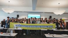 event 2025 KAIST Global Entrepreneurship Summer School Concludes Successfully in Silicon Valley
The “2025 KAIST Global Entrepreneurship Summer School (2025 KAIST GESS),” organized by the Office of Global Initiative of the KAIST International Office (Vice President So Young Kim), successfully concluded. Now in its fourth year, the program was designed to provide KAIST students with firsthand experience of the world’s leading startup ecosystem in Silicon Valley, USA, and to strengthen ...
-
 research KAIST Enhances Immunotherapy for Difficult-to-Treat Brain Tumors with Gut Microbiota
Advanced treatments, known as immunotherapies that activate T cells—our body's immune cells—to eliminate cancer cells, have shown limited efficacy as standalone therapies for glioblastoma, the most lethal form of brain tumor. This is due to their minimal response to glioblastoma and high resistance to treatment.
-
-
-
 research High-Resolution Spectrometer that Fits into Smartphones Developed by KAIST Researchers
Color, as the way light\`s wavelength is perceived by the human eye, goes beyond a simple aesthetic element, containing important scientific information like a substance\`s composition or state. Spectrometers are optical devices that analyze material properties by decomposing light into its constituent wavelengths, and they are widely used in various scientific and industrial fields, including m...
-
 research KAIST Identifies Master Regulator Blocking Immunotherapy, Paving the Way for a New Lung Cancer Treatment
KAIST researchers have discovered that \`DEAD-box helicases 54 (DDX54)\`, a type of RNA-binding protein, is the master regulator that hinders the effectiveness of immunotherapy—opening a new path for lung cancer treatment.
-
-
 research KAIST Directly Visualizes the Hidden Spatial Order of Electrons in a Quantum Material
<(Back row, from left) Yeongkwan Kim, SungBin Lee, Heejun Yang, Yongsoo Yang_(Front row, from left) Jemin Park, Seokjo Hong, Jaewhan Oh> · Cryogenic 4D-STEM reveals how charge density waves form, fragment, and persist across a phase transition · First direct measurement of electronic amplitude correlations uncovers strain-driven inhomogeneity and localized order above the transition temperature Electronic order in quantum materials often emerges not uniformly, but through subtle and complex patterns that vary from place to place. One prominent example is the charge density wave (CDW), an ordered state in which electrons arrange themselves into periodic patterns at low temperatures. Although CDWs have been studied for decades, how their strength and spatial coherence evolve across a phase transition has remained largely inaccessible experimentally. Now, a team led by Professor Yongsoo Yang of the Department of Physics at KAIST (Korea Advanced Institute of Science and Technology), together with Professors SungBin Lee, Heejun Yang, and Yeongkwan Kim, and in collaboration with Stanford University, has for the first time directly visualized the spatial evolution of charge density wave amplitude order inside a quantum material. A New Way to See Electronic Order at the Nanoscale Using a liquid-helium-cooled electron microscope setup combined with four-dimensional scanning transmission electron microscopy (4D-STEM), the researchers mapped how CDW order develops, weakens, and fragments as temperature changes. This approach allowed them to reconstruct nanoscale maps of the CDW amplitude, revealing not just whether the order exists, but how strong it is and how it is spatially connected. This study is similar to filming the growth of ice crystals as water freezes using an ultra-high-magnification camera. In this case, however, the researchers observed electrons arranging themselves at cryogenic temperatures of around –253°C, and used an electron microscope capable of resolving features one hundred-thousandth the width of a human hair instead of a conventional camera. The results showed that the electronic patterns do not appear uniformly across the material. In some regions, clear patterns are visible, while in neighboring areas they are entirely absent, much like a lake that does not freeze all at once, with patches of ice interspersed with liquid water. How Electronic Order Breaks Apart in Real Space The team further demonstrated that this spatial inhomogeneity is closely linked to local strain inside the crystal. Even extremely small distortions that are far below optical resolution strongly suppress the CDW amplitude. This clear anticorrelation between strain and electronic order provides direct evidence that local lattice distortions play a decisive role in shaping CDW patterns. Unexpectedly, the researchers also observed that localized regions of CDW order can persist even above the transition temperature, where long-range order is generally thought to disappear. These isolated pockets of electronic order suggest that the CDW transition is not a simple, uniform melting process, but instead involves gradual loss of spatial coherence. A key advance of this work is the world’s first direct measurement of CDW amplitude correlations. By quantifying how the strength of electronic order at one location is related to that at another, the study reveals how CDW coherence collapses across the transition, while local amplitude remains finite. Such information could not be obtained with conventional diffraction or scanning probe techniques. Toward a New Framework for Studying Electronic Order Charge density waves are a central feature of many quantum materials and often coexist or compete with other electronic states. By directly accessing their spatial structure and correlations, this study provides a new experimental framework for understanding how collective electronic order forms and evolves in real materials. Dr. Yongsoo Yang, who led the research, explained the significance of the results: “Until now, the spatial coherence of charge density waves was largely inferred indirectly. Our approach allows us to directly visualize how electronic order varies across space and temperature, and to identify the factors that locally stabilize or suppress it.” [Figure 1] Schematic illustration of an experiment employing 4D-STEM to probe the spatial variations of charge density waves in the prototypical quantum material NbSe2 under a liquid-helium cryogenic environment (AI-generated image). This research, with Seokjo Hong, Jaewhan Oh and Jemin Park of KAIST as co-first authors, was published online in Physical Review Letters on January 6th (Title: Spatial correlations of charge density wave order across the transition in 2H-NbSe2). The study was mainly supported by the National Research Foundation of Korea (NRF) Grants (Individual Basic Research Program, Basic Research Laboratory Program, Nanomaterial Technology Development Program) funded by the Korean Government (MSIT).
-
 research Seeing Black Holes More Clearly with Laser Light
<(From Left) Researcher Junyong Choi, Researcher Woosong Jeong, Professor Jungwon Kim, Researcher Jihoon Baek > Radio telescopes are instruments that capture faint radio signals from space and convert them into images of celestial bodies. To observe distant black holes clearly, multiple radio telescopes must capture cosmic signals at exactly the same time, acting as a single unit. Research teams at KAIST have developedr a new reference signal technology that uses laser light to precisely synchronize the observation timing and phase of these telescopes. KAIST announced on January 15th that a research team led by Professor Jungwon Kim from the Department of Mechanical Engineering—in collaboration with the Korea Astronomy and Space Science Institute, the Korea Research Institute of Standards and Science, and the Max Planck Institute for Radio Astronomy (MPIfR) in Germany—has implemented a technology that directly applies optical frequency comb lasers to radio telescope receivers. While a typical laser emits only one color (frequency), an optical frequency comb laser emits tens of thousands of extremely accurate colors arranged at regular intervals. This appearance resembles the teeth of a comb, hence the name "frequency comb." Since the frequency of each individual "tooth" is known exactly and the intervals can be precision-tuned to the level of an atomic clock, scientists refer to it as an "ultra-precision ruler made of light." The core of Very Long Baseline Interferometry (VLBI), a technique where multiple radio telescopes observe simultaneously, is aligning the phases of the radio signals received by each telescope as if aligning them to a single precise ruler. However, existing electronic reference signal methods faced limitations; as observation frequencies increased, precise phase calibration is becoming more difficult. In response, the KAIST research team developed a method to deliver the optical frequency comb laser directly into the radio telescope, based on the idea of "improving the fundamental precision of phase alignment by utilizing light (lasers) from the signal generation stage." Through this, they successfully solved the problems of reference signal generation and phase calibration simultaneously within a single optical system. If the conventional method was like using a "ruler that makes phase alignment difficult" at higher frequencies, this new technology can be compared to setting a standard with an "ultra-precision ruler that fixes the phase with extremely stable light." As a result, they have laid the foundation for distant radio telescopes to interoperate as elaborately as one giant telescope. This technology was verified through test observations at the Korea VLBI Network (KVN) Yonsei Radio Telescope. The research team succeeded in detecting stable interference patterns (fringes) between radio telescopes and proved through actual observation that precise phase calibration is possible. Recently, this system was also installed at the KVN SNU Pyeongchang Radio Telescope, leading to expanded experiments using multiple observation sites simultaneously. The team expects that this will not only allow for clearer imaging of black holes but also drastically reduce phase delay errors between instruments—a long-standing issue in VLBI observations. The applications of this technology are not limited to astronomical observations. The team anticipates that it can be expanded to various advanced fields requiring precise space-time measurements, such as▲ Intercontinental ultra-precision clock comparison ▲Space geodesy ▲Deep-space probe tracking < Illustration of the system principle (Image generated by AI) > Professor Jungwon Kim of KAIST stated, "This research is a case where the limits of existing electronic signal generation technology were overcome by directly applying optical frequency comb lasers to radio telescopes. It will significantly contribute to improving the precision of next-generation black hole observations and advancing the fields of frequency metrology and time standards." Dr. Minji Hyun (currently at KRISS) and Dr. Changmin Ahn from KAIST participated as co-first authors. The research findings were published on January 4th in the international academic journal Light: Science & Applications. Paper Title: Optical frequency comb integration in radio telescopes: advancing signal generation and phase calibration DOI: 10.1038/s41377-025-02056-w Lead Authors: Dr. Minji Hyun (KAIST, currently KRISS), Dr. Changmin Ahn (KAIST), Jungwon Kim (KAIST) This research was conducted with support from the National Research Council of Science & Technology (NST) Creative Alliance Project(CAP), the National Research Foundation of Korea (NRF), and the Institute of Information & Communications Technology Planning & Evaluation (IITP).
-
 research Breaking the 1% Barrier, KAIST Boosts Brightness of Eco-Friendly Ultra-Small Semiconductors by 18-Fold
<(Front rwo, from left) KAIST co-first author Changhyun Joo, co-first author Seongbeom Yeon, (Back row, from left) Jaeyoung Ha, Professor Himchan Cho, Jaedong Jang> Light-emitting semiconductors are used throughout everyday life in TVs, smartphones, and lighting. However, many technical barriers remain in developing environmentally friendly semiconductor materials. In particular, nanoscale semiconductors that are tens of thousands of times smaller than the width of a human hair (about 100,000 nanometers) are theoretically capable of emitting bright light, yet in practice have suffered from extremely weak emission. KAIST researchers have now developed a new surface-control technology that overcomes this limitation. KAIST (President Kwang Hyung Lee) announced on the 14th of January that a research team led by Professor Himchan Cho of the Department of Materials Science and Engineering has developed a fundamental technology to control, at the atomic level, the surface of indium phosphide (InP)* magic-sized clusters (MSCs)—nanoscale semiconductor particles regarded as next-generation eco-friendly semiconductor materials.* Indium phosphide (InP): a compound semiconductor made of indium (In) and phosphorus (P), considered an environmentally friendly alternative that does not use hazardous elements such as cadmium The material studied by the team is known as a magic-sized cluster, an ultrasmall semiconductor particle composed of only several tens of atoms. Because all particles have identical size and structure, these materials are theoretically capable of emitting extremely sharp and pure light. However, due to their extremely small size of just 1–2 nanometers, even minute surface defects cause most of the emitted light to be lost. As a result, luminescence efficiency has remained below 1% to date. Previously, this issue was addressed by etching the surface with strong chemicals such as hydrofluoric acid (HF). However, the overly aggressive reactions often damaged the semiconductor itself. Professor Cho’s team adopted a different approach. Instead of removing the surface all at once, they devised a precision etching strategy that allows chemical reactions to proceed in a highly controlled, incremental manner. This enabled selective removal of only the defect sites that hindered light emission, while preserving the overall structure of the semiconductor. During this defect-removal process, fluorine generated by the reaction combined with zinc species in the solution to form zinc chloride, which in turn stabilized and passivated the exposed nanocrystal surface. < Schematic illustration of overcoming emission efficiency limits via atomic-scale precision control > As a result, the research team increased the luminescence efficiency of the semiconductor from below 1% to 18.1%. This represents the highest reported performance to date among indium phosphide–based ultrasmall nanosemiconductors, corresponding to an 18-fold increase in brightness. This study is particularly significant in that it demonstrates, for the first time, that the surfaces of ultrasmall semiconductors—previously considered nearly impossible to control—can be precisely engineered at the atomic level. The technology is expected to find applications not only in next-generation displays, but also in advanced fields such as quantum communication and infrared sensing. < Eco-friendly Ultra-compact Semiconductor Chemical Reaction (AI-generated image) > Professor Himchan Cho explained, “This work is not simply about making brighter semiconductors, but about demonstrating how critical atomic-level surface control is for achieving desired performance.” This research was carried out with Changhyun Joo, a doctoral student, and Seongbeom Yeon, a combined master’s-doctoral student in the Department of Materials Science and Engineering at KAIST, serving as co–first authors. Professor Himchan Cho and Professor Ivan Infante of the Basque Center for Materials, Applications, and Nanostructures (BCMaterials, Spain) participated as co-corresponding authors. The study was published online on December 16 in the Journal of the American Chemical Society (JACS), one of the most prestigious journals in chemistry. ※ Paper title: “Overcoming the Luminescence Efficiency Limitations of InP Magic-Sized Clusters,” DOI: 10.1021/jacs.5c13963 This research was supported by the National Research Foundation of Korea through the Nano Materials Technology Development Program, the Next-Generation Intelligent Semiconductor Technology Development Program, the Quantum Information Science Human Infrastructure Program, and by the Korea Basic Science Institute through its Infrastructure Support Program for Early-Career Researchers.
-
 research KAIST Proposes AI-Driven Strategy to Solve Long-Standing Mystery of Gene Function
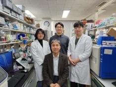
<(From Left) Distinguisehd Professor Sang Yup Lee, Dr. Gi Bae Kim, Professor Bernhard O. Palsson> “We know the genes, but not their functions.” To resolve this long-standing bottleneck in microbial research, a joint research team has proposed a cutting-edge research strategy that leverages Artificial Intelligence (AI) to drastically accelerate the discovery of microbial gene functions. KAIST announced on January 12th that a research team led by Distinguished Professor Sang Yup Lee from the Department of Chemical and Biomolecular Engineering, in collaboration with Professor Bernhard Palsson from the Department of Bioengineering at UCSD, has published a comprehensive review paper. The study systematically analyzes and organizes the latest AI-based research approaches aimed at revolutionizing the speed of gene function discovery. Since the early 2000s, when whole-genome sequencing became a reality, there were high expectations that the genetic blueprint of life would be fully decoded. However, even twenty years later, the roles of a significant portion of genes within microbial genomes remain unknown. While various experimental methods—such as gene deletion, analysis of gene expression profiles, and in vitro activity assays—have been employed, discovering gene functions remains a time-consuming and costly endeavor. This is primarily due to the limitations of large-scale experimentation, complex biological interactions, and the discrepancy between laboratory results and actual in vivo responses. To overcome these hurdles, the research team emphasized that an AI-driven approach combining computational biology with experimental biology is essential. In this paper, the team provides a comprehensive overview of computational biology approaches that have facilitated gene function discovery, ranging from traditional sequence similarity analysis to the latest deep-learning-based AI models. Notably, 3D protein structure prediction technologies such as AlphaFold (developed by Google DeepMind) and RoseTTAFold (developed by the University of Washington) have opened new doors. These tools go beyond simple functional estimation, offering the potential to understand the underlying mechanisms of how gene functions operate. Furthermore, generative AI is now extending research boundaries toward designing proteins with specifically desired functions. Focusing on transcription factors (proteins that act as genetic switches) and enzymes (proteins that catalyze chemical reactions), the team presented various application cases and future research directions that integrate gene sequence analysis, protein structure prediction, and diverse metagenomic analyses. <Schematic illustration of computational biology methods for enzyme function prediction>
-
 research KAIST Develops OLED Technology with Double the Screen Brightness
<(From Left) Ph.D candidate Minjae Kim, Professor Seunghyup Yoo, Dr. Junho Kim> Organic light-emitting diodes (OLEDs) are widely used in smartphones and TVs thanks to their excellent color reproduction and thin, flexible planar structure. However, internal light loss has limited further improvements in brightness. KAIST researchers have now developed a technology that more than doubles OLED light-emission efficiency while maintaining the flat structure that is a key advantage of OLED displays. KAIST (President Kwang Hyung Lee) announced on the 11th of January that a research team led by Professor Seunghyup Yoo of the School of Electrical Engineering has developed a new near-planar light outcoupling structure* and an OLED design method that can significantly reduce light loss inside OLED devices.* Near-planar light outcoupling structure: a thin structure that keeps the OLED surface almost flat while extracting more of the light generated inside to the outside OLEDs are composed of multiple layers of ultrathin organic films stacked on top of one another. As light passes through these layers, it is repeatedly reflected or absorbed, often causing more than 80% of the light generated inside the OLED to be lost as heat before it can escape. To address this issue, light outcoupling structures such as hemispherical lenses or microlens arrays (MLAs) have been used to extract light from OLEDs. However, hemispherical lenses protrude significantly, making it difficult to maintain a flat form factor, while MLAs must cover much larger area than individual pixel sizes to achieve sufficient light extraction. This creates limitations in achieving high efficiency without interference between neighboring pixels. To increase OLED brightness while preserving a planar structure, the research team proposed a new OLED design strategy that maximizes light extraction within the size of each individual pixel. Unlike conventional designs that assume OLEDs extend infinitely, this approach takes into account the finite pixel sizes actually used in real displays. As a result, more light can be emitted externally even from pixels of the same size. In addition, the team developed a new near-planar light outcoupling structure that helps light emerge efficiently in the forward direction without being spread too widely. This structure is very thin—comparable in thickness to existing microlens arrays—yet achieves light extraction efficiency close to that of hemispherical lenses of the same lateral dimension. As a result, it hardly undermines the flat form factors of OLEDs and can be readily applied to flexible OLED displays. By combining the new OLED design with the near-planar light outcoupling structure, the researchers successfully achieved more than a twofold improvement in light-emission efficiency even in small pixels. < Quasi-Planar Light Extraction OLED Technology > This technology enables brighter displays using the same power while maintaining OLED’s flat structure, and is expected to extend battery life and reduce heat generation in mobile devices such as smartphones and tablets. Improvements in display lifespan are also anticipated. MinJae Kim, the first author of the study, noted, “A small idea that came up during class was developed into real research results through the KAIST Undergraduate Research Program (URP).” Professor Seunghyup Yoo stated, “Although many light outcoupling structures have been proposed, most were designed for large-area lighting applications, and many were difficult to apply effectively to displays composed of numerous small pixels,” adding, “The near-planar light outcoupling structure proposed in this work was designed with constraints on the size of the light source within each pixel, reducing optical interference between adjacent pixels while maximizing efficiency.” He further emphasized that the approach can be applied not only to OLEDs but also to next-generation display technologies based on materials such as perovskites and quantum dots. < Schematic Overview and Application Examples of the Proposed Light Extraction Structure > This research, with MinJae Kim (Department of Materials Science and Engineering, KAIST; currently a Ph.D. student in Materials Science and Engineering at Stanford University) and Junho Kim (School of Electrical Engineering, KAIST; currently a postdoctoral researcher at the University of Cologne, Germany) as co–first authors, was published online on December 29, 2025, in Nature Communications. ※ Paper title: “Near-planar light outcoupling structures with finite lateral dimensions for ultra-efficient and optical crosstalk-free OLED displays” DOI: 10.1038/s41467-025-66538-6 This research was supported by the KAIST Undergraduate Research Program (URP), the Mid-Career Researcher Program and the Future Display Strategic Research Lab Program of the National Research Foundation (NRF) of Korea, the Human Resource Development Program of the Korea Institute for Advancement of Technology (KIAT), and the Korea Planning & Evaluation Institute of Industrial Technology (KEIT).
-
 event KAIST Proposes a Multinational AI Cooperation Strategy Beyond U.S.–China Dominance
 -
 event Selection of the 'Proud Alumni Award' Recipients
<(From left) Donggeun Yoo, CAIO of Lunit / Eun-kang Song, CEO of Capstone Partners / Sang Ouk Kim, Professor of Materials Science and Engineering at KAIST/ Sung-soo Kim, Special Professor at Yonsei University/ Byung Jin Cho, Professor of Electrical Engineering at KAIST/ Joongi Kim, CTO of Lablup> KAIST announced on January 16th that the Alumni Association has selected the recipients of the 'KAIST Proud Alumni Award.' Starting this year, the 'KAIST Proud Alumni Award' has been expanded and reorganized into six categories—Innovative Entrepreneurship, Industrial Contribution, Academic Research, Public Innovation, Social Service, and Young Alumni—to broadly highlight the achievements of alumni active in various fields. The award ceremony will be held at the '2026 KAIST New Year's Gala' at 5 p.m. on the 16th at the EL Tower in Seoul. Donggeun Yoo, Chief Artificial Intelligence Officer (CAIO) of Lunit Inc. (B.S. 2011, M.S. 2013, Ph.D. 2019, School of Electrical Engineering), was selected as the recipient of the Innovative Entrepreneurship category. CAIO Yoo co-founded Lunit, a first-generation deep learning AI startup in Korea, in 2013, leading AI technology in the field of cancer diagnosis and treatment. Recently, he contributed to strengthening national competitiveness in the medical AI industry by leading the 'AI-specialized Foundation Model Project.' In the Industrial Contribution category, Eun-kang Song, CEO of Capstone Partners (M.S. 1988, School of Computing), was named. CEO Song is the person who established the early-stage investment-centered strategy in the domestic venture capital industry. Over the past 28 years, he has led the development of the venture ecosystem by growing companies into unicorns through more than 200 investments. The recipient of the Academic Research category, Sang Ouk Kim, Professor of Materials Science and Engineering at KAIST (B.S. 1994, M.S. 1996, Ph.D. 2000, Dept. of Chemical and Biomolecular Engineering), opened a new horizon in new material research by identifying the liquid crystallinity of graphene oxide for the first time in the world. This research is evaluated as a core original technology that enabled the mass production of high-purity graphene, serving as an example of the industrial expansion of basic research. The Public Innovation category was awarded to Sung-soo Kim, Special Professor at the College of Engineering, Yonsei University (former Chairman of the Science and Technology Professionals Community) (Ph.D. 1988, Dept. of Chemistry). During his tenure as the Vice Minister of Science, Technology, and Innovation, Professor Kim established a pan-governmental technology self-reliance system for materials, parts, and equipment in response to Japanese export restrictions and led the innovation of national R&D governance. Byung Jin Cho, Professor of the School of Electrical Engineering at KAIST (M.S. 1987, Ph.D. 1991, School of Electrical Engineering), was selected for the Social Service category. Since founding a campus club in 2010, Professor Cho has practiced continuous mentoring and sharing for 15 years, supporting the academic studies and settlement of international students. Joongi Kim, Chief Technology Officer (CTO) and co-founder of Lablup Inc. (B.S. 2010, M.S. 2012, Ph.D. 2016, School of Computing), who received the Young Alumni award given to talents aged 40 or younger, developed an open-source-based AI infrastructure management platform and proved technological competitiveness in the global market by registering core GPU fractional virtualization technology as patents in Korea, the U.S., and Japan. Kwang Hyung Lee, President of KAIST, said, "This year's awardees are role models for KAISTians who have contributed to the development of society and the nation with outstanding achievements. These challenges and achievements of our seniors will inspire juniors and contribute to spreading the innovative values of KAIST." Yun-tae Lee, the 27th President of the KAIST Alumni Association, stated, "The six awardees are the protagonists who have practiced the values of KAISTians across academia, industry, public, and society. The Alumni Association will continue to serve as a link for the achievements of alumni to spread into society." Meanwhile, the newly elected 28th President of the Alumni Association, Hoo-sik Kim, is scheduled to begin his term in February 2026.
-
 event Playground for Future Quantum Technology: KAIST-MIT Quantum Information Winter School Successfully Concluded
< Group photo of the KAIST-MIT Quantum Information Winter School > “Through the KAIST-MIT Quantum Information Winter School, I was able to view research from a broader perspective. The experience of collaborating with students from various universities and majors to complete a project was very refreshing,” said Jun-hyeong Cho, a student at the KAIST School of Electrical Engineering. KAIST announced on the 16th that the Graduate School of Quantum Science and Technology successfully concluded the ‘KAIST-MIT Quantum Information Winter School,’ held jointly with the Massachusetts Institute of Technology (MIT) from January 5th to 16th at the KAIST main campus in Daejeon. For this year’s Winter School, 50 junior and senior undergraduate students from Korea and abroad were selected to receive intensive training to grow into next-generation quantum talent. Eight world-renowned scholars from KAIST and MIT participated in the program, providing a multi-dimensional curriculum that spanned theory and practice—ranging from theoretical lectures and introductions to cutting-edge quantum experiments to visits to government-funded research institutes and student poster presentations. Celebrating its third anniversary since its inception in 2024, the Winter School is now evaluated as a premier quantum information education program in Korea. Alongside KAIST faculty, world-class scholars from MIT participated directly in lectures and field training, operating an intensive curriculum that covered the entirety of quantum information science. The lecturing faculty included world authorities in quantum computing, quantum devices, quantum machine learning, and quantum simulation, such as MIT professors Pablo Jarillo-Herrero, Seth Lloyd, Kevin P. O’Brien, and William D. Oliver, as well as KAIST scholars Jaewook Ahn, Joonwoo Bae, Gil-Young Cho, and Jae-yoon Choi. Going beyond theoretical lectures, participants gained a broad understanding of research trends, technical limitations, and future development directions of state-of-the-art quantum technology through experimental training in core areas such as quantum computing, communication, sensing, and simulation. < Scene from a Winter School lecture > Furthermore, students visited the Korea Research Institute of Standards and Science (KRISS) and the Electronics and Telecommunications Research Institute (ETRI) to experience actual research sites, engaging in field-oriented education that bridges quantum theory and practice. The poster presentation session, where students shared their own research ideas, received enthusiastic responses as a forum for deep academic exchange, allowing students to receive direct feedback from MIT faculty. Tae-hee Kim, a student from Pusan National University, remarked, “I was greatly inspired by the passion of the MIT faculty and the high level of questions from the students. It served as a motivation for me to pursue deeper studies independently.” Byung-jin Hwang, a student from Yonsei University, added, “I expected lectures from world-class scholars to be difficult, but I was impressed by the explanations tailored to the undergraduate level. The poster presentation session was particularly memorable.” Eun-seong Kim, Dean of the KAIST Graduate School of Quantum Science and Technology, stated, “The KAIST-MIT Quantum Information Winter School is a special educational program where students can learn directly from world-renowned quantum researchers and experience cutting-edge research. We look forward to the active participation of future talents who will lead the quantum industry.” Participants for this Winter School were selected through a document review process, and the program was operated entirely free of charge. KAIST covered all educational expenses and provided dormitory accommodations and lunch. Detailed information about the event can be found on the KAIST Graduate School of Quantum Science and Technology website (https://quantumschool.kaist.ac.kr/). < Poster for the KAIST-MIT Quantum Information Winter School >
-
 event Chairman Jae-Chul Kim of Dongwon Group Donates a Total of 60.3 Billion Won to KAIST
<Jae-Chul Kim, Honorary Chairman of Dongwon Group> "In the era of AI, a new future lies within the sea of data. I ask that KAIST leaps forward to become the world's No. 1 AI research group." — Jae-Chul Kim, Honorary Chairman of Dongwon Group KAIST announced on January 16th that Honorary Chairman Jae-Chul Kim of Dongwon Group has pledged an additional 5.9 billion KRW in development funds to foster Artificial Intelligence (AI) talent and strengthen research infrastructure, bringing his total contribution to 60.3 billion KRW. This marks his second additional donation since 2020, continuing his steadfast support for strengthening South Korea's national competitiveness in the field of AI. Through his initial donation in 2020, Chairman Kim established the 'Kim Jaechul Graduate School of AI' at KAIST, urging the university to secure world-class capabilities. Upon hearing that KAIST’s AI research level ranked 5th among global universities over the past five years (2020–2024), Chairman Kim requested that the university strive to reach the No. 1 spot in the world. In response, President Kwang Hyung Lee explained, "To surpass Carnegie Mellon University (CMU), which is currently evaluated as the world’s best with an AI faculty of about 45, the KAIST Graduate School of AI needs to expand its faculty to over 50 and construct a dedicated research building." Chairman Kim responded by saying, "I will build the building," and this latest donation is a fulfillment of that promise. This third pledge of 5.9 billion KRW was decided to cover the projected budget shortfall as the design of the AI Education and Research Building enters full-scale development. The AI Education and Research Building will be a facility with 8 floors above ground and 1 basement level, covering a total floor area of 18,182 m² (approx. 5,500 pyeong). It is scheduled for completion in February 2028. Once finished, it will serve as a global AI research hub housing 50 faculty members and 1,000 students. Since the 2021 academic year, KAIST has been selecting 60 Master’s and 10 Doctoral students annually as 'Dongwon Scholars' outside of the regular quota for a period of 10 years. While the tuition and research incentives for the first three years were supported by the donation, KAIST has been utilizing its own budget since the 2024 academic year to ensure students can focus entirely on their research. Moving forward, the Kim Jaechul Graduate School of AI plans to build a world-class faculty and operate systematic Master's and Doctoral programs to cultivate global AI leaders. In addition to technical expertise, the school will offer educational programs focused on character and holistic development, leading the charge in strengthening Korea's AI competitiveness. Honorary Chairman Jae-Chul Kim stated, "I hope this donation serves as a small 'priming water' for South Korea to leap forward as an AI powerhouse. I look forward to seeing global core talents grow here and contribute to our national strength." President Kwang Hyung Lee expressed his gratitude, saying, "Chairman Kim’s unwavering support is the greatest driving force for KAIST to secure global AI sovereignty. We will ensure the Kim Jaechul Graduate School of AI becomes a mecca where the world's best AI minds gather to innovate, honoring the Chairman’s vision."
-
 event KAIST–Daekyo, Opening of the Cognitive Enhancement Research Center Lounge
< Group photo of officials at the opening ceremony of the KAIST–Daekyo Cognitive Enhancement Research Center Lounge > KAIST held the opening ceremony for the ‘KAIST–Daekyo Cognitive Enhancement Research Center Lounge,’ jointly established with Daekyo, at the Meta-Convergence Hall on the Daejeon main campus last Saturday, the 10th. This lounge was established through an in-kind donation by Daekyo for space creation as part of research cooperation. It was designed as a base space to more systematically operate brain development and cognitive function enhancement research that KAIST and Daekyo have been jointly promoting, and to share research results with society. Through this event, KAIST introduced the achievements of its research cooperation to date and provided a forum to explore the future directions of education and brain science. Key KAIST officials, including Kyun Min Lee, Vice President for Provost and Academic Affairs, and Dae-Soo Kim, Dean of the College of Life Science and Bioengineering, as well as officials from both organizations, including Ho-joon Kang, CEO of Daekyo, attended the event to celebrate the opening of the lounge. Since signing a Memorandum of Understanding (MOU) for industry-academic research cooperation with Daekyo in 2023, our university has been jointly conducting research on cognitive function enhancement and mental health across the entire life cycle—from infants to adults and seniors—based on brain and cognitive science. The cooperation continues to expand these research results into educational content and solutions. An official from Daekyo stated, "The Cognitive Enhancement Research Center Lounge is a symbolic space for the research cooperation accumulated by both organizations, and it is highly meaningful to be able to communicate directly with customers and share research results here. Moving forward, Daekyo will continue to expand its cooperation with KAIST to prove the value of scientific and systematic education." Kyun Min Lee, Vice President for Provost and Academic Affairs, said, "The opening of this lounge is significant in that a space for industry-academic cooperation research was created through Daekyo’s donation. Based on this space, KAIST will strive to share the achievements of brain and cognitive science research with society and contribute to the field of education."
-
 DongA Science Quantum Computers are a Moneymaker, Call for Infrastructure Support for Software Companies
//m.dongascience.com/en/news/74899
2025.11.06 -
PHYS ORG Room temperature 3D printing enables miniaturized infrared sensors
//phys.org/news/2025-11-room-temperature-3d-enables-miniaturized.html
2025.11.03 -
Maeil Business Newspaer When CEO NVIDIA Jensen Hwang expressed his willingness to cooperate
//www.mk.co.kr/en/business/11457572
2025.11.02 -
The Asia Business Daily "Completed in 10 Minutes" KAIST Develops Ultra-Fast Sintering Process for Green Hydrogen...
//cm.asiae.co.kr/en/article/2025102808175075633
2025.10.28 -
Aju Press Global AI Frontier Symposium brings together world leaders in Seoul
//www.ajupress.com/view/20251027155244888
2025.10.27
-
PR Office
A Lunar Exploration Wheel Inspired by Origami. Korea's Journey to the Moon Has Just Begun | Prof. Dae-Young Lee, Researcher Seong-Bin Lee
2026-01-07 -
PR Office
From Ordering Goods to Booking Trains: An AI That Does Everything With Just a Word, Not a Touch / Prof. Insik Shin, Researcher Youngmin Im, Researcher Jaeyoung Wi
2025-12-09