nanotechnology
-
 New Chiral Nanostructures to Extend the Material Platform
Researchers observed a wide window of chiroptical activity from nanomaterials
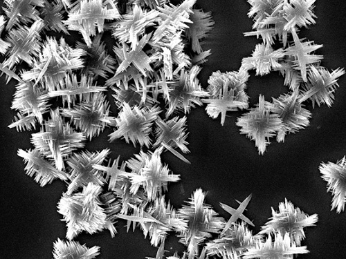
A research team transferred chirality from the molecular scale to a microscale to extend material platforms and applications. The optical activity from this novel chiral material encompasses to short-wave infrared region.
This platform could serve as a powerful strategy for hierarchical chirality transfer through self-assembly, generating broad optical activity and providing immense applications including bio, telecommunication, and imaging technique. This is the first observation of such a wide window of chiroptical activity from nanomaterials.
“We synthesized chiral copper sulfides using cysteine, as the stabilizer, and transferring the chirality from molecular to the microscale through self-assembly,” explained Professor Jihyeon Yeom from the Department of Materials Science and Engineering, who led the research. The result was reported in ACS Nano on September 14.
Chiral nanomaterials provide a rich platform for versatile applications. Tuning the wavelength of polarization rotation maxima in the broad range is a promising candidate for infrared neural stimulation, imaging, and nanothermometry. However, the majority of previously developed chiral nanomaterials revealed the optical activity in a relatively shorter wavelength range, not in short-wave infrared.
To achieve chiroptical activity in the short-wave infrared region, materials should be in sub-micrometer dimensions, which are compatible with the wavelength of short-wave infrared region light for strong light-matter interaction. They also should have the optical property of short-wave infrared region absorption while forming a structure with chirality.
Professor Yeom’s team induced self-assembly of the chiral nanoparticles by controlling the attraction and repulsion forces between the building block nanoparticles. During this process, molecular chirality of cysteine was transferred to the nanoscale chirality of nanoparticles, and then transferred to the micrometer scale chirality of nanoflowers with 1.5-2 2 μm dimensions formed by the self-assembly.
“We will work to expand the wavelength range of chiroptical activity to the short-wave infrared region, thus reshaping our daily lives in the form of a bio-barcode that can store vast amount of information under the skin,” said Professor Yeom.
This study was funded by the Ministry of Science and ICT, the Ministry of Health and Welfare, the Ministry of Food and Drug Safety, the National Research Foundation of Korea,the KAIST URP Program, the KAIST Creative Challenging Research Program, Samsung and POSCO Science Fellowship.
-PublicationKi Hyun Park, Junyoung Kwon, Uichang Jeong, Ji-Young Kim, Nicholas A.Kotov, Jihyeon Yeom, “Broad Chrioptical Activity from Ultraviolet to Short-Wave Infrared by Chirality Transfer from Molecular to Micrometer Scale," September 14, 2021 ACS Nano (https://doi.org/10.1021/acsnano.1c05888)
-ProfileProfessor Jihyeon YeomNovel Nanomaterials for New Platforms LaboratoryDepartment of Materials Science and EngineeringKAIST
2021.10.22 View 7908
 -
 ACS Nano Special Edition Highlights Innovations at KAIST
- The collective intelligence and technological innovation of KAIST was highlighted with case studies including the Post-COVID-19 New Deal R&D Initiative Project. -
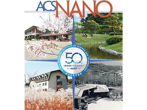
KAIST’s innovative academic achievements and R&D efforts for addressing the world’s greatest challenges such as the COVID-19 pandemic were featured in ACS Nano as part of its special virtual issue commemorating the 50th anniversary of KAIST. The issue consisted of 14 review articles contributed by KAIST faculty from five departments, including two from Professor Il-Doo Kim from the Department of Materials Science and Engineering, who serves as an associate editor of the ACS Nano.
ACS Nano, the leading international journal in nanoscience and nanotechnology, published a special virtual issue last month, titled ‘Celebrating 50 Years of KAIST: Collective Intelligence and Innovation for Confronting Contemporary Issues.’
This special virtual issue introduced KAIST’s vision of becoming a ‘global value-creative leading university’ and its progress toward this vision over the last 50 years. The issue explained how KAIST has served as the main hub for advanced scientific research and technological innovation in South Korea since its establishment in 1971, and how its faculty and over 69,000 graduates played a key role in propelling the nation’s rapid industrialization and economic development.
The issue also emphasized the need for KAIST to enhance global cooperation and the exchange of ideas in the years to come, especially during the post-COVID era intertwined with the Fourth Industrial Revolution (4IR). In this regard, the issue cited the first ‘KAIST Emerging Materials e-Symposium (EMS)’, which was held online for five days in September of last year with a global audience of over 10,000 participating live via Zoom and YouTube, as a successful example of what academic collaboration could look like in the post-COVID and 4IR eras.
In addition, the “Science & Technology New Deal Project for COVID-19 Response,” a project conducted by KAIST with support from the Ministry of Science and ICT (MSIT) of South Korea, was also introduced as another excellent case of KAIST’s collective intelligence and technological innovation. The issue highlighted some key achievements from this project for overcoming the pandemic-driven crisis, such as: reusable anti-virus filters, negative-pressure ambulances for integrated patient transport and hospitalization, and movable and expandable negative-pressure ward modules.
“We hold our expectations high for the outstanding achievements and progress KAIST will have made by its centennial,” said Professor Kim on the background of curating the 14 review articles contributed by KAIST faculty from the fields of Materials Science and Engineering (MSE), Chemical and Biomolecular Engineering (CBE), Nuclear and Quantum Engineering (NQE), Electrical Engineering (EE), and Chemistry (Chem).
Review articles discussing emerging materials and their properties covered photonic carbon dots (Professor Chan Beum Park, MSE), single-atom and ensemble catalysts (Professor Hyunjoo Lee, CBE), and metal/metal oxide electrocatalysts (Professor Sung-Yoon Chung, MSE).
Review articles discussing materials processing covered 2D layered materials synthesis based on interlayer engineering (Professor Kibum Kang, MSE), eco-friendly methods for solar cell production (Professor Bumjoon J. Kim, CBE), an ex-solution process for the synthesis of highly stable catalysts (Professor WooChul Jung, MSE), and 3D light-patterning synthesis of ordered nanostructures (Professor Seokwoo Jeon, MSE, and Professor Dongchan Jang, NQE).
Review articles discussing advanced analysis techniques covered operando materials analyses (Professor Jeong Yeong Park, Chem), graphene liquid cell transmission electron microscopy (Professor Jong Min Yuk, MSE), and multiscale modeling and visualization of materials systems (Professor Seungbum Hong, MSE).
Review articles discussing practical state-of-the-art devices covered chemiresistive hydrogen sensors (Professor Il-Doo Kim, MSE), patient-friendly diagnostics and implantable treatment devices (Professor Steve Park, MSE), triboelectric nanogenerators (Professor Yang-Kyu Choi, EE), and next-generation lithium-air batteries (Professor Hye Ryung Byon, Chem, and Professor Il-Doo Kim, MSE).
In addition to Professor Il-Doo Kim, post-doctoral researcher Dr. Jaewan Ahn from the KAIST Applied Science Research Institute, Dean of the College of Engineering at KAIST Professor Choongsik Bae, and ACS Nano Editor-in-Chief Professor Paul S. Weiss from the University of California, Los Angeles also contributed to the publication of this ACS Nano special virtual issue.
The issue can be viewed and downloaded from the ACS Nano website at https://doi.org/10.1021/acsnano.1c01101.
Image credit: KAIST
Image usage restrictions: News organizations may use or redistribute this image,with proper attribution, as part of news coverage of this paper only.
Publication:
Ahn, J., et al. (2021) Celebrating 50 Years of KAIST: Collective Intelligence and Innovation for Confronting Contemporary Issues. ACS Nano 15(3): 1895-1907. Available online at https://doi.org/10.1021/acsnano.1c01101
Profile:
Il-Doo Kim, Ph.D
Chair Professor
idkim@kaist.ac.kr
http://advnano.kaist.ac.kr
Advanced Nanomaterials and Energy Lab.
Department of Materials Science and Engineering
Membrane Innovation Center for Anti-Virus and Air-Quality Control
https://kaist.ac.kr/
Korea Advanced Institute of Science and Technology (KAIST) Daejeon, Republic of Korea
(END)
2021.03.05 View 24893
 -
 Ultrathin but Fully Packaged High-Resolution Camera
- Biologically inspired ultrathin arrayed camera captures super-resolution images. -
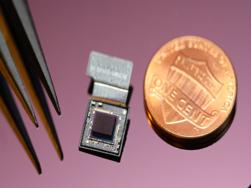
The unique structures of biological vision systems in nature inspired scientists to design ultracompact imaging systems. A research group led by Professor Ki-Hun Jeong have made an ultracompact camera that captures high-contrast and high-resolution images. Fully packaged with micro-optical elements such as inverted micro-lenses, multilayered pinhole arrays, and gap spacers on the image sensor, the camera boasts a total track length of 740 μm and a field of view of 73°.
Inspired by the eye structures of the paper wasp species Xenos peckii, the research team completely suppressed optical noise between micro-lenses while reducing camera thickness. The camera has successfully demonstrated high-contrast clear array images acquired from tiny micro lenses. To further enhance the image quality of the captured image, the team combined the arrayed images into one image through super-resolution imaging.
An insect’s compound eye has superior visual characteristics, such as a wide viewing angle, high motion sensitivity, and a large depth of field while maintaining a small volume of visual structure with a small focal length. Among them, the eyes of Xenos peckii and an endoparasite found on paper wasps have hundreds of photoreceptors in a single lens unlike conventional compound eyes. In particular, the eye structures of an adult Xenos peckii exhibit hundreds of photoreceptors on an individual eyelet and offer engineering inspiration for ultrathin cameras or imaging applications because they have higher visual acuity than other compound eyes.
For instance, Xenos peckii’s eye-inspired cameras provide a 50 times higher spatial resolution than those based on arthropod eyes. In addition, the effective image resolution of the Xenos peckii’s eye can be further improved using the image overlaps between neighboring eyelets. This unique structure offers higher visual resolution than other insect eyes.
The team achieved high-contrast and super-resolution imaging through a novel arrayed design of micro-optical elements comprising multilayered aperture arrays and inverted micro-lens arrays directly stacked over an image sensor. This optical component was integrated with a complementary metal oxide semiconductor image sensor.
This is first demonstration of super-resolution imaging which acquires a single integrated image with high contrast and high resolving power reconstructed from high-contrast array images. It is expected that this ultrathin arrayed camera can be applied for further developing mobile devices, advanced surveillance vehicles, and endoscopes.
Professor Jeong said, “This research has led to technological advances in imaging technology. We will continue to strive to make significant impacts on multidisciplinary research projects in the fields of microtechnology and nanotechnology, seeking inspiration from natural photonic structures.”
This work was featured in Light Science & Applications last month and was supported by the National Research Foundation (NRF) of and the Ministry of Health and Welfare (MOHW) of Korea.
Image credit: Professor Ki-Hun Jeong, KAIST
Image usage restrictions: News organizations may use or redistribute this image, with proper attribution, as part of news coverage of this paper only.
Publication:
Kisoo Kim, Kyung-Won Jang, Jae-Kwan Ryu, and Ki-Hun Jeong. (2020) “Biologically inspired ultrathin arrayed camera for high-contrast and high-resolution imaging”. Light Science & Applications. Volume 9. Article 28. Available online at https://doi.org/10.1038/s41377-020-0261-8
Profile:
Ki-Hun Jeong
Professor
kjeong@kaist.ac.kr
http://biophotonics.kaist.ac.kr/
Department of Bio and Brain Engineering
KAIST
Profile:
Kisoo Kim
Ph.D. Candidate
kisoo.kim1@kaist.ac.kr
http://biophotonics.kaist.ac.kr/
Department of Bio and Brain Engineering
KAIST
(END)
2020.03.23 View 15054
 -
 Ultrafast Quantum Motion in a Nanoscale Trap Detected
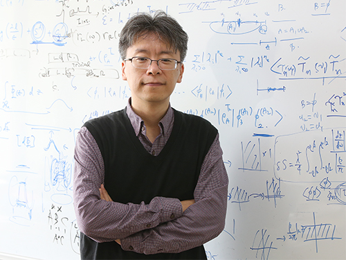
< Professor Heung-Sun Sim (left) and Co-author Dr. Sungguen Ryu (right) >
KAIST researchers have reported the detection of a picosecond electron motion in a silicon transistor. This study has presented a new protocol for measuring ultrafast electronic dynamics in an effective time-resolved fashion of picosecond resolution. The detection was made in collaboration with Nippon Telegraph and Telephone Corp. (NTT) in Japan and National Physical Laboratory (NPL) in the UK and is the first report to the best of our knowledge.
When an electron is captured in a nanoscale trap in solids, its quantum mechanical wave function can exhibit spatial oscillation at sub-terahertz frequencies. Time-resolved detection of such picosecond dynamics of quantum waves is important, as the detection provides a way of understanding the quantum behavior of electrons in nano-electronics. It also applies to quantum information technologies such as the ultrafast quantum-bit operation of quantum computing and high-sensitivity electromagnetic-field sensing. However, detecting picosecond dynamics has been a challenge since the sub-terahertz scale is far beyond the latest bandwidth measurement tools.
A KAIST team led by Professor Heung-Sun Sim developed a theory of ultrafast electron dynamics in a nanoscale trap, and proposed a scheme for detecting the dynamics, which utilizes a quantum-mechanical resonant state formed beside the trap. The coupling between the electron dynamics and the resonant state is switched on and off at a picosecond so that information on the dynamics is read out on the electric current being generated when the coupling is switched on.
NTT realized, together with NPL, the detection scheme and applied it to electron motions in a nanoscale trap formed in a silicon transistor. A single electron was captured in the trap by controlling electrostatic gates, and a resonant state was formed in the potential barrier of the trap.
The switching on and off of the coupling between the electron and the resonant state was achieved by aligning the resonance energy with the energy of the electron within a picosecond. An electric current from the trap through the resonant state to an electrode was measured at only a few Kelvin degrees, unveiling the spatial quantum-coherent oscillation of the electron with 250 GHz frequency inside the trap.
Professor Sim said, “This work suggests a scheme of detecting picosecond electron motions in submicron scales by utilizing quantum resonance. It will be useful in dynamical control of quantum mechanical electron waves for various purposes in nano-electronics, quantum sensing, and quantum information”.
This work was published online at Nature Nanotechnology on November 4. It was partly supported by the Korea National Research Foundation through the SRC Center for Quantum Coherence in Condensed Matter. For more on the NTT news release this article, please visit https://www.ntt.co.jp/news2019/1911e/191105a.html
-ProfileProfessor Heung-Sun Sim
Department of PhysicsDirector, SRC Center for Quantum Coherence in Condensed Matterhttps://qet.kaist.ac.kr KAIST
-Publication:Gento Yamahata, Sungguen Ryu, Nathan Johnson, H.-S. Sim, Akira Fujiwara, and Masaya Kataoka. 2019. Picosecond coherent electron motion in a silicon single-electron source. Nature Nanotechnology (Online Publication). 6 pages. https://doi.org/10.1038/s41565-019-0563-2
2019.11.05 View 15616
 -
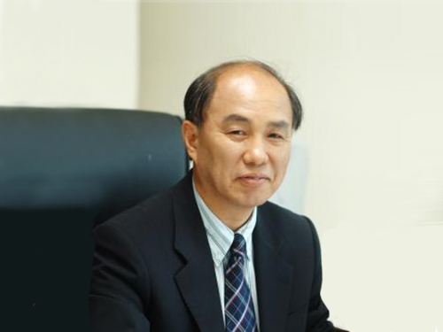 Chair Professor Jo-Won Lee Named Sixth President of National Nano Fab Center
< President Jo-Won Lee >
Chair professor Jo-Won Lee from Hanyang University was appointed as the sixth president of the National Nano Fab Center (NNFC). President Lee will serve his term for three years from September 16.
The NNFC is an affiliated institution of KAIST, established in 2002 to foster qualified manpower in the field of nanotechnology (NT) in Korea. The NNFC features cutting-edge NT-related research equipment and fabrication services, and provides students and researchers quality education and training. The NNFC seeks to become a world-leading institute by performing extensive business operations including the commercialization of NT research results and conducting various multidisciplinary projects.
President Lee received his BS degree from Hanyang University and his MS and PhD degrees in metals science from the Pennsylvania State University. He taught nano-conversion science at his alma mater, Hanyang University, while serving as the director of the National Program for Tera-level Nanodevices. President Lee also guided the governmental planning committee for the 10-year Korea Nanotechnology Initiative as secretary general.
President Lee said, “The NNFC has been striving to develop Korea as the world’s strongest nation in nanotechnology thus far. All of the members of the NNFC will continue giving our best effort for the improvement of our nation’s nanotechnology.”
(END)
2019.09.17 View 3250
 -
 KAIST and the University of Minnesota-Twin Cities Partner for Research and Education Collaboration
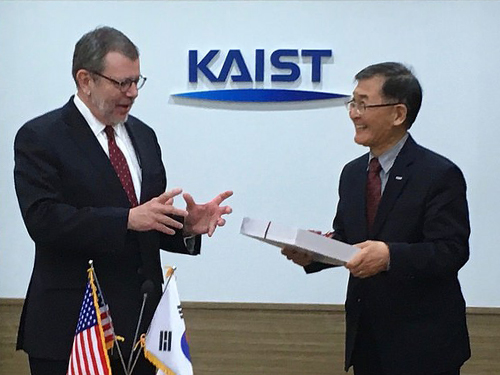
President Steve Kang of KAIST and President Eric W. Kaler of the University of Minnesota-Twin Cities (United States) signed a memorandum of understanding to create exchange programs for students and faculty and to conduct joint research in the field of health and food. The following is an excerpt from President Kaler’s blog (https://storify.com/UMNstory/globalumn-hksk#edaadf) on his visit of KAIST on November 18, 2015:
A visit to the Korea Advanced Institute of Science and Technology
About 90 miles from Seoul—and more than that two-and-a-half-hours of a bus ride through the rugged early-morning traffic of South Korea’s capital city—sits Daejeon, Korea’s sixth largest city and home to KAIST, the Korea Advanced Institute of Science and Technology. Today, President Kaler and the small University of Minnesota delegation accompanying him visited what’s considered Korea’s MIT, a place focused on research and known to push the limits toward the future.
Fingernail heart monitors? Wireless anesthetic-monitoring devices?
KAIST is working on them.
The overlap of interests—from biomedical engineering to nanotechnology to robotics—between KAIST (pronounced “Kyst”) and the U are remarkable. Smartphone apps to monitor human health and GPS-driven robots to serve military interests or deliver packages were among the developing inventions that KAIST scientists showed to Kaler.
And even the personal relationships seem to illustrate the cliché of a small world and the natural affinity of Minnesota and KAIST.
KAIST’s President Sang Mo Kang was once the head of the University of Illinois’ department of electrical and computer engineering, and he and Kaler—a renowned chemical engineer before becoming the U’s president—hit it off … despite disagreeing about the potential outcome of Saturday’s Illinois-Gophers football game.
Accompanying Kaler on the day’s journey, meetings, and signing of a Memorandum of Understanding between the two schools to advance collaborations was U Associate Professor Sang Hyun Oh. Oh happens to be a physics graduate of this very KAIST and is now a rising star in Minnesota’s Department of Electrical and Computer Engineering.
The two sides agreed to focus on matching scholars on their respective campuses to discuss the sorts of research the two institutions can partner on. The idea of “Grand Challenges,” at the core of the U’s Twin Cities campus Strategic Plan, has fascinated Korean higher education leaders during Kaler’s weeklong visit, and KAIST’s leadership was interested in the health and food research, two U strengths.
###
2015.12.04 View 7403
 -
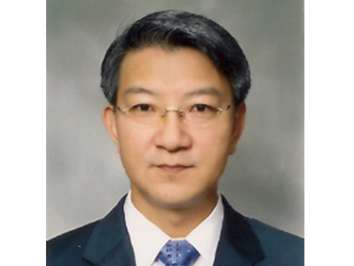 Distinguished Professor Sang Yup Lee Participates in the 2014 Summer Davos Forum
Distinguished Professor Sang Yup Lee from the Department of Chemical and Biomolecular Engineering, KAIST, was invited to lead four sessions at the Annual Meeting 2014, the World Economic Forum, also known as the Summer Davos Forum, which was held in Tianjin, China, from September 10th to 12th.
Two of the four sessions Professor Lee participated in were held on September 10th. At the first session entitled “Biotechnology Ecosystem,” he examined with other panelists the future of bioengineering in depth and discussed major policies and industry trends that will be necessary for the development of future biotechnologies.
Professor Lee later attended the “Strategic Shifts in Healthcare” session as a moderator. Issues related to transforming the health industry such as the next-generation genomics, mobile health and telemedicine, and wearable devices and predictive analytics were addressed.
On September 12, Professor Lee joined the “IdeasLab with KAIST” and gave a presentation on nanotechnology. There was a total of ten IdeasLab sessions held at the Summer Davos Forum, and KAIST was the only Korean university ever invited to host this session. In addition to Professor Lee’s presentation, three more presentations were made by KAIST professors on such topics as “Sustainable Energy and Materials” and “Next-generation Semiconductors.”
Lastly, Professor Lee participated in the “Global Promising Technology” session with the World Economic Forum’s Global Agenda Council members. At this session, he explained the selection of the “World’s Top 10 Most Promising Technologies” and “Bio Sector’s Top 10 Technologies” and led discussions about the “2015 Top 10 Technologies” with the council members.
The Davos Forum has been announcing the “World’s Top 10 Most Promising Technologies” since 2012, and Professor Lee has played a key role in the selection while working as the Chairman of Global Agenda Council. The selection results are presented at the Davos Forum every year and have attracted a lot of attention from around the world.
2014.09.15 View 10601
 -
 DNA based semiconductor technology developed
Professor Park Hyun Gyu’s research team from the Department of Chemical and Biomolecular Engineering at KAIST has successfully implemented all logic gates using DNA, a feat that led the research to be published as the cover paper for the international nanotechnology paper "Small".
Even with the latest technology, it was impossible to create a silicon based semiconductor smaller than 10nm, but because DNA has a thickness of only 2nm, this could lead to the creation of semiconductors with groundbreaking degrees of integration.
A 2 nm semiconductor will be able to store 10,000 HD movies within a size of a postage stamp, at least 100 times more than the current 20nm semiconductors.
DNAs are comprised of 4 bases which are continually connected: Adenine (A) with Thymine (T), and Guanine (G) with Cytosine (C).
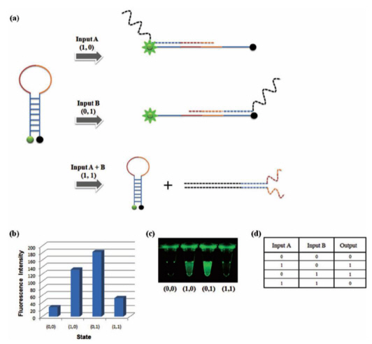
For this research, the team used the specific binding properties of DNA, which forms its helix-shape, and a circular molecular beacon that has fluorescent signaling properties under structural changes.
The research team used input signals to open and close the circular DNA, the same principle that is applied to logic gates in digital circuits.
The output signal was measured using the increase and decrease of the fluorescent signal from the molecular beacon due to the opening and closing of the circular DNA respectively.
The team overcame the limited system problems of the existing logic gates and managed to implement all 8 logic gates (AND, OR, XOR, INHIBIT, NAND, NOR, XNOR, IMPlCATION). A multilevel circuit that connects different logic gates was also tested to show its regenerative properties.
Professor Park said that “cheap bio-electric devices with high degrees of integration will be made possible by this research” and that “there will be a large difference in the field of molecular level electronic research”
Mr. Park Gi Su, a doctoral candidate and the 1st author of this research, said that “a DNA sequence of 10 bases is only 3.4nm long and 2nm thick, which can be used to effectively increase the degree of integration of electronic devices” and that “a bio computer could materialize in the near future through DNA semiconductors with accurate logic gates”.
XOR Gate: The output signal 1 comes through the open circular DNA when either input DNA A or input DNA B is present. When both inputs are not present, the flourescent signal does not come through
2012.09.27 View 9007
 -
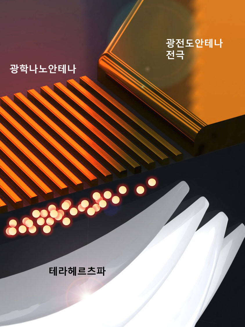 The output of terahertz waves enhanced by KAIST team
KAIST researchers have greatly improved the output of terahertz waves, the blue ocean of the optics world. This technology is expected to be applied to portable X-ray cameras, small bio-diagnostic systems, and in many other devices.
Professor Ki-Hun Jeong"s research team from the Department of Bio and Brain Engineering used optical nano-antenna technology to increase the output of terahertz waves by three times.
Terahertz waves are electromagnetic waves with frequencies between 100GHz to 30THz. They are produced when a femtosecond (10^-15 s) pulse laser is shone on a semiconductor substrate with photoconduction antennas, causing a photocurrent pulse of one picosecond (10^-12 s). Their long wavelengths, in comparison to visible light and infrared rays, give terahertz waves a high penetration power with less energy than X-rays, making them less harmful to humans.
These qualities allow us to see through objects, just as X-rays do, but because terahertz waves absorb certain frequencies, we can detect hidden explosives or drugs, which was not possible with X-rays. We can even identify fake drugs. Furthermore, using the spectral information, we can analyze a material"s innate qualities without chemical processing, making it possible to identify skin diseases without harming the body. However, the output was not sufficient to be used in biosensors and other applications.
Prof. Jeong"s team added optical nano-antennas, made from gold nano-rods, in between the photoconduction antennas and optimized the structure. This resulted in nanoplasmonic resonance in the photoconduction substrate, increasing the degree of integration of the photocurrent pulse and resulting in a three times larger output.
Hence, it is not only possible to see through objects more clearly, but it is also possible to analyze components without a biopsy.
Professor Jeong explained, "This technology, coupled with the miniaturization of terahertz devices, can be applied to endoscopes to detect early epithelial cancer" and that he will focus on creating and commercializing these biosensor systems.
This research was published in the March issue of the international nanotechnology journal ACS Nano and was funded by the Korea Evaluation Institute of Industrial Technology and the National Research Foundation of Korea.
Figure: Mimetic diagram of a THz generator with nano-antennas
2012.04.29 View 11215
 -
 10 Technolgies to Change the World in 2012: The Future Technology Global Agenda Council
The Future Technology Global Agenda Council which is under the World Economy Forum and which KAIST’s biochemical engineering department’s Prof. Sang Yeob Lee is the head of, chose the 10 new technologies that will change the world in year 2012.
The ten technologies include: IT, synthetic biology and metabolic engineering, Green Revolution 2.0, material construction nanotechnology, systematic biology and the simulation technology of biological systems, the technology to use CO2 as a natural resource, wireless power transmission technology, high density energy power system, personalized medical/nutritional/disease preventing system, and new education technology.
The technologies were chosen on the basis of the opinions various science, industry, and government specialists and is deemed to have high potential to change the world in the near future.
The Future Technology Global Agenda Council will choose ten new technologies yearly starting this year in order to solve the problems the world now faces.
The informatics systems that was ranked 1st place, sifts only the data necessary for decision making out of the overflowing amount of data. Much interest has been spurred at the Davos forum.
The synthetic biology and metabolic engineering chosen is expected to play an important role in creating new medicines and producing chemical substances and materials from reusable resources.
Biomass has also been chosen as one of the top ten most important technologies as it was seen to be necessary to lead the second Green Revolution in order to stably provide food for the increasing population and to create bio refineries.
Nanomaterials structured at the molecular level are expected to help us solve problems regarding energy, food, and resources.
Systematic biology and computer modeling is gaining importance in availing humans to construct efficient remedies, materials, and processes while causing minimum effects on the environment, resource reserves, and other people.
The technology to convert CO2, which is considered a problem all over the world, into a useful resource is also gaining the spotlight
Together with such technologies, wireless power transmission technology, high density energy power system, personalized medical/nutritional/disease preventing system, and new education technology are also considered the top ten technologies to change the world.
Prof. Lee said, “Many new discoveries are being made due to the accelerating rate of technological advancements. Many of the technologies that the council has found are sustainable and important for the construction of our future.”
2012.04.04 View 10217
 -
 Closer to the Dream: Graphene
A technique that allows easy and larger observation area of graphene’s crystal face was developed by Korean Research Team.
The research team, led by Professor Jeong Hui Tae (KAIST), consists of Doctorate candidate Kim Dae Woo, Dr. Kim Yoon Ho (primary author), Doctorate candidate Jeong Hyun Soo. The research is supported by WCU (World Class Research University) Development Plan, Mid-Aged Researcher Support Business and was published in the online edition of Nature Nanotechnology.
(Dissertation: Direct visualization of large0area graphene domains and boundaries by optical birefringency)
Professor Jeong’s team used the optical property of the liquid display used in LCD to visualize the size and shape of the single crystals along a flat surface. The visualization of the single crystal allowed the measurement of a near theoretical value of electrical conductivity of graphene.
Graphene has great electrical conductivity, transparent, mechanically stable, flexible, and is therefore regarded as the next generation electrical material. However the polycrystalinity of graphene meant that the actual electrical, mechanical properties were lower than the theoretical values. The reason was thought to be because of the size of the crystal faces and boundary structures.
Therefore, in order to create graphene that has good properties, observing the domain and boundary of graphene crystal faces is essential.
The new technique developed by the research team is another step towards commercializing transparent electrodes, flexible display, and electric materials like solar cells.
2012.01.31 View 9512
 -
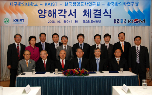 KAIST, KRIBB Agree to Cooperate in Research of Convergence Technologies
Oct. 15, 2008 -- KAIST and Korea Research Institute of Bioscience and Biotechnology (KRIBB) have agreed to cooperate in the research of convergence fields of biotechnology, information technology and nanotechnology.
To this end, the two institutions concluded a memorandum of understanding to create a new academia-institute cooperative model in the convergence fields on Oct. 15 in Seoul, with KAIST President Nam-Pyo Suh, KRIBB Director Young-Hoon Park and Vice Minister of Education, Science and Technology Jong-Koo Park in attendance.
Under the agreement, the two institutions will set up the tentatively-named KAIST-KRIBB BINT Convergence Institute for the development of technologies and nurturing skilled manpower in the convergence fields.
The partnership of the two institutions is expected to bring broad-based cooperation opportunities and create a massive synergy effect by combining their resources and infrastructure for the development of convergence technologies, KAIST officials said..
The proposed institute is also designed to build a world-class research hub in systems biotechnology by combining strengths of the two institutions with initiatives to achieve the Korean government"s new vision for "low carbon, green growth."
The institute will also serve as a base for domestic brain convergence by concentrating the nation"s research capacities in genetics and brain technology.
KAIST also signed a memorandum of understanding for cooperation in researches in Oriental medicine with three institutions, KRIBB, Daegu Hanny University and Korea Institute of Oriental Medicine.
The agreement calls for the four institutions to conduct joint researches in traditional sciences and Oriental medicine based on systems biology, develop manpower in related fields and share academic and research information.
The agreement is expected to provide impetus to reinforcing competitiveness in compound and convergence technologies and discover new properties in Oriental medicine, according to KAIST authorities.
2008.10.16 View 14749