science
-
 KAIST Develops Customized Tactile Sensor That Can Detect Light Breath, Pressure and Sound
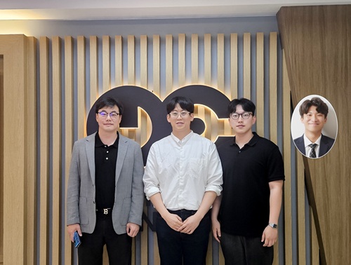
< Photo 1. (From left) Professor Inkyu Park of KAIST Department of Mechanical Engineering (ME), Dr. Jungrak Choi of ETRI, Ph.D. Candidate Donho Lee and M.S. Graduate Chankyu Han of KAIST ME >
When a robot grabs an object or a medical device detects a pulse, the tactile sensor is the technology that senses pressure like a fingertip. Existing sensors had disadvantages, such as slow responses or declining accuracy after repeated use, but Korean researchers have succeeded in developing a sensor that can quickly and accurately detect even light breath, pressure, and sound. This sensor can be used across a broad range — from everyday movements to medical diagnostics.
KAIST (represented by President Kwang Hyung Lee) announced on the 23rd of June that Professor Inkyu Park’s team from the Department of Mechanical Engineering, through a collaborative research project with the Electronics and Telecommunications Research Institute (ETRI, President Seung Chan Bang ) under the National Research Council of Science & Technology (NST, Chairman Young Sik Kim), has developed an innovative technology that overcomes the structural limitations of existing tactile sensors.
The core of this joint research is the implementation of a customized tactile sensor that simultaneously achieves flexibility, precision, and repeatable durability by applying Thermoformed 3D Electronics (T3DE).
< Figure 1. Comparative evaluation of soft elastomer–based 3D structure versus thermoforming-based 3D structure in terms of mechanical properties. >
In particular, soft elastomer-based sensors (rubber, silicone, etc. — materials that stretch and return to their original shape) have structural problems such as slow response times, high hysteresis*, and creep**, but this new platform operates precisely in diverse environments and overcomes these limitations.
*Hysteresis: A phenomenon where the previously applied force or change is retained like a “memory,” so that the same stimulus does not always produce the same result.
**Creep: The phenomenon where a material slowly deforms when a force is continuously applied.
T3DE sensors are manufactured by precisely forming electrodes on a 2D film, then thermoforming them into a 3D structure under heat and pressure. Specifically, the top electrodes and supporting pillar structures of the sensor are designed to allow the fine-tuning of the mechanical properties for different purposes. By adjusting microstructural parameters — such as the thickness, length, and number of support pillars — the sensor’s Young’s modulus* can be tuned across a broad range of 10 Pa to 1 MPa. This matches the stiffness of biological tissues like skin, muscle, and tendons, making them highly suitable as bio-interface sensors.
*Young’s modulus: An index representing a material's stiffness; this research can control this index to match various biological tissues.
The newly developed T3DE sensor uses air as a dielectric material to reduce power consumption and demonstrates outstanding performance in sensitivity, response time, thermal stability, and repeatable accuracy.
Experimental results showed that the sensor achieved △sensitivity of 5,884 kPa⁻¹, △response time of 0.1 ms (less than one-thousandth of a second), △hysteresis of less than 0.5%, and maintained a repeatable precision of 99.9% or higher even after 5,000 repeated measurements.
< Figure 2. Graphic Overview of thermoformed 3D electronics (T3DE) >
The research team also constructed a high-resolution 40×70 array, comprising a total of 2,800 densely packed sensors, to visualize the pressure distribution on the sole of the foot in real time during exercise and confirmed the possibility of using the sensor for wrist pulse measurement to assess vascular health. Furthermore, successful results were also achieved in sound-detection experiments at a level comparable to commercial acoustic sensors. In short, the sensor can precisely and quickly measure foot pressure, pulse, and sound, allowing it to be applied in areas such as sports, health, and sound sensing.
The T3DE technology was also applied to an augmented-reality(AR)-based surgical training system. By adjusting the stiffness of each sensor element to match that of biological tissues, the system provided real-time visual and tactile feedback according to the pressure applied during surgical incisions. It also offered real-time warnings if an incision was too deep or approached a risky area, making it a promising technology for enhancing immersion and accuracy in medical training.
KAIST Professor Inkyu Park stated, “Because this sensor can be precisely tuned from the design stage and operates reliably across diverse environments, it can be used not only in everyday life, but also in a variety of fields such as healthcare, rehabilitation, and virtual reality.”
The research was co-led as first authors by Dr. Jungrak Choi of ETRI, KAIST master’s student Chankyu Han, and Ph.D. candidate Donho Lee, under the overall guidance of Professor Inkyu Park. The research results were published in the May 2025 issue of ‘Science Advances’ and introduced to the global research community through the journal’s official SNS channels (Facebook, Twitter).
※ Thesis Title: Thermoforming 2D films into 3D electronics for high-performance, customizable tactile sensing
※ DOI: 10.1126/sciadv.adv0057
< Figure 3. The introduction of the study on the official SNS posting by Science Advances >
This research was supported by the Ministry of Trade, Industry and Energy, the National Research Foundation of Korea, and the Korea Institute for Advancement of Technology.
2025.06.23 View 186
KAIST Develops Customized Tactile Sensor That Can Detect Light Breath, Pressure and Sound
< Photo 1. (From left) Professor Inkyu Park of KAIST Department of Mechanical Engineering (ME), Dr. Jungrak Choi of ETRI, Ph.D. Candidate Donho Lee and M.S. Graduate Chankyu Han of KAIST ME >
When a robot grabs an object or a medical device detects a pulse, the tactile sensor is the technology that senses pressure like a fingertip. Existing sensors had disadvantages, such as slow responses or declining accuracy after repeated use, but Korean researchers have succeeded in developing a sensor that can quickly and accurately detect even light breath, pressure, and sound. This sensor can be used across a broad range — from everyday movements to medical diagnostics.
KAIST (represented by President Kwang Hyung Lee) announced on the 23rd of June that Professor Inkyu Park’s team from the Department of Mechanical Engineering, through a collaborative research project with the Electronics and Telecommunications Research Institute (ETRI, President Seung Chan Bang ) under the National Research Council of Science & Technology (NST, Chairman Young Sik Kim), has developed an innovative technology that overcomes the structural limitations of existing tactile sensors.
The core of this joint research is the implementation of a customized tactile sensor that simultaneously achieves flexibility, precision, and repeatable durability by applying Thermoformed 3D Electronics (T3DE).
< Figure 1. Comparative evaluation of soft elastomer–based 3D structure versus thermoforming-based 3D structure in terms of mechanical properties. >
In particular, soft elastomer-based sensors (rubber, silicone, etc. — materials that stretch and return to their original shape) have structural problems such as slow response times, high hysteresis*, and creep**, but this new platform operates precisely in diverse environments and overcomes these limitations.
*Hysteresis: A phenomenon where the previously applied force or change is retained like a “memory,” so that the same stimulus does not always produce the same result.
**Creep: The phenomenon where a material slowly deforms when a force is continuously applied.
T3DE sensors are manufactured by precisely forming electrodes on a 2D film, then thermoforming them into a 3D structure under heat and pressure. Specifically, the top electrodes and supporting pillar structures of the sensor are designed to allow the fine-tuning of the mechanical properties for different purposes. By adjusting microstructural parameters — such as the thickness, length, and number of support pillars — the sensor’s Young’s modulus* can be tuned across a broad range of 10 Pa to 1 MPa. This matches the stiffness of biological tissues like skin, muscle, and tendons, making them highly suitable as bio-interface sensors.
*Young’s modulus: An index representing a material's stiffness; this research can control this index to match various biological tissues.
The newly developed T3DE sensor uses air as a dielectric material to reduce power consumption and demonstrates outstanding performance in sensitivity, response time, thermal stability, and repeatable accuracy.
Experimental results showed that the sensor achieved △sensitivity of 5,884 kPa⁻¹, △response time of 0.1 ms (less than one-thousandth of a second), △hysteresis of less than 0.5%, and maintained a repeatable precision of 99.9% or higher even after 5,000 repeated measurements.
< Figure 2. Graphic Overview of thermoformed 3D electronics (T3DE) >
The research team also constructed a high-resolution 40×70 array, comprising a total of 2,800 densely packed sensors, to visualize the pressure distribution on the sole of the foot in real time during exercise and confirmed the possibility of using the sensor for wrist pulse measurement to assess vascular health. Furthermore, successful results were also achieved in sound-detection experiments at a level comparable to commercial acoustic sensors. In short, the sensor can precisely and quickly measure foot pressure, pulse, and sound, allowing it to be applied in areas such as sports, health, and sound sensing.
The T3DE technology was also applied to an augmented-reality(AR)-based surgical training system. By adjusting the stiffness of each sensor element to match that of biological tissues, the system provided real-time visual and tactile feedback according to the pressure applied during surgical incisions. It also offered real-time warnings if an incision was too deep or approached a risky area, making it a promising technology for enhancing immersion and accuracy in medical training.
KAIST Professor Inkyu Park stated, “Because this sensor can be precisely tuned from the design stage and operates reliably across diverse environments, it can be used not only in everyday life, but also in a variety of fields such as healthcare, rehabilitation, and virtual reality.”
The research was co-led as first authors by Dr. Jungrak Choi of ETRI, KAIST master’s student Chankyu Han, and Ph.D. candidate Donho Lee, under the overall guidance of Professor Inkyu Park. The research results were published in the May 2025 issue of ‘Science Advances’ and introduced to the global research community through the journal’s official SNS channels (Facebook, Twitter).
※ Thesis Title: Thermoforming 2D films into 3D electronics for high-performance, customizable tactile sensing
※ DOI: 10.1126/sciadv.adv0057
< Figure 3. The introduction of the study on the official SNS posting by Science Advances >
This research was supported by the Ministry of Trade, Industry and Energy, the National Research Foundation of Korea, and the Korea Institute for Advancement of Technology.
2025.06.23 View 186 -
 High-Resolution Spectrometer that Fits into Smartphones Developed by KAIST Researchers
- Professor Mooseok Jang's research team at the Department of Bio and Brain Engineering develops an ultra-compact, high-resolution spectrometer using 'double-layer disordered metasurfaces' that generate unique random patterns depending on light's color.
- Unlike conventional dispersion-based spectrometers that were difficult to apply to portable devices, this new concept spectrometer technology achieves 1nm-level high resolution in a device smaller than 1cm, comparable in size to a fingernail.
- It can be utilized as a built-in spectrometer in smartphones and wearable devices in the future, and can be expanded to advanced optical technologies such as hyperspectral imaging and ultrafast imaging.
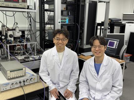
< Photo 1. (From left) Professor Mooseok Jang, Dong-gu Lee (Ph.D. candidate), Gookho Song (Ph.D. candidate) >
Color, as the way light's wavelength is perceived by the human eye, goes beyond a simple aesthetic element, containing important scientific information like a substance's composition or state. Spectrometers are optical devices that analyze material properties by decomposing light into its constituent wavelengths, and they are widely used in various scientific and industrial fields, including material analysis, chemical component detection, and life science research. Existing high-resolution spectrometers were large and complex, making them difficult for widespread daily use. However, thanks to the ultra-compact, high-resolution spectrometer developed by KAIST researchers, it is now expected that light's color information can be utilized even within smartphones or wearable devices.
KAIST (President Kwang Hyung Lee) announced on the 13th that Professor Mooseok Jang's research team at the Department of Bio and Brain Engineering has successfully developed a reconstruction-based spectrometer technology using double-layer disordered metasurfaces*.
*Double-layer disordered metasurface: An innovative optical device that complexly scatters light through two layers of disordered nanostructures, creating unique and predictable speckle patterns for each wavelength.
Existing high-resolution spectrometers have a large form factor, on the order of tens of centimeters, and require complex calibration processes to maintain accuracy. This fundamentally stems from the operating principle of traditional dispersive elements, such as gratings and prisms, which separate light wavelengths along the propagation direction, much like a rainbow separates colors. Consequently, despite the potential for light's color information to be widely useful in daily life, spectroscopic technology has been limited to laboratory or industrial manufacturing environments.
< Figure 1. Through a simple structure consisting of a double layer of disordered metasurfaces and an image sensor, it was shown that speckles of predictable spectral channels with high spectral resolution can be generated in a compact form factor. The high similarity between the measured and calculated speckles was used to solve the inverse problem and verify the ability to reconstruct the spectrum. >
The research team devised a method that departs from the conventional spectroscopic paradigm of using diffraction gratings or prisms, which establish a one-to-one correspondence between light's color information and its propagation direction, by utilizing designed disordered structures as optical components. In this process, they employed metasurfaces, which can freely control the light propagation process using structures tens to hundreds of nanometers in size, to accurately implement 'complex random patterns (speckle*)'.
*Speckle: An irregular pattern of light intensity created by the interference of multiple wavefronts of light.
Specifically, they developed a method that involves implementing a double-layer disordered metasurface to generate wavelength-specific speckle patterns and then reconstructing precise color information (wavelength) of the light from the random patterns measured by a camera.
As a result, they successfully developed a new concept spectrometer technology that can accurately measure light across a broad range of visible to infrared (440-1,300nm) with a high resolution of 1 nanometer (nm) in a device smaller than a fingernail (less than 1cm) using only a single image capture.
< Figure 2. A disordered metasurface is a metasurface with irregularly arranged structures ranging from tens to hundreds of nanometers in size. In a double-layer structure, a propagation space is placed between the two metasurfaces to control the output speckle with high degrees of freedom, thereby achieving a spectral resolution of 1 nm even in a form factor smaller than 1 cm. >
Dong-gu Lee, a lead author of this study, stated, "This technology is implemented in a way that is directly integrated with commercial image sensors, and we expect that it will enable easy acquisition and utilization of light's wavelength information in daily life when built into mobile devices in the future."
Professor Mooseok Jang said, "This technology overcomes the limitations of existing RGB three-color based machine vision fields, which only distinguish and recognize three color components (red, green, blue), and has diverse applications. We anticipate various applied research for this technology, which expands the horizon of laboratory-level technology to daily-level machine vision technology for applications such as food component analysis, crop health diagnosis, skin health measurement, environmental pollution detection, and bio/medical diagnostics." He added, "Furthermore, it can be extended to various advanced optical technologies such as hyperspectral imaging, which records wavelength and spatial information simultaneously with high resolution, 3D optical trapping technology, which precisely controls light of multiple wavelengths into desired forms, and ultrafast imaging technology, which captures phenomena occurring in very short periods."
This research was collaboratively led by Dong-gu Lee (Ph.D. candidate) and Gookho Song (Ph.D. candidate) from the KAIST Department of Bio and Brain Engineering as co-first authors, with Professor Mooseok Jang as the corresponding author. The findings were published online in the international journal Science Advances on May 28, 2025.* Paper Title: Reconstructive spectrometer using double-layer disordered metasurfaces* DOI: 10.1126/sciadv.adv2376
This research was supported by the Samsung Research Funding and Incubation Center of Samsung Electronics grant, the National Research Foundation of Korea (NRF) grant funded by the Korea government (MSIT), and the Bio & Medical Technology Development Program of the National Research Foundation (NRF) funded by the Korean government (MSIT).
2025.06.13 View 981
High-Resolution Spectrometer that Fits into Smartphones Developed by KAIST Researchers
- Professor Mooseok Jang's research team at the Department of Bio and Brain Engineering develops an ultra-compact, high-resolution spectrometer using 'double-layer disordered metasurfaces' that generate unique random patterns depending on light's color.
- Unlike conventional dispersion-based spectrometers that were difficult to apply to portable devices, this new concept spectrometer technology achieves 1nm-level high resolution in a device smaller than 1cm, comparable in size to a fingernail.
- It can be utilized as a built-in spectrometer in smartphones and wearable devices in the future, and can be expanded to advanced optical technologies such as hyperspectral imaging and ultrafast imaging.
< Photo 1. (From left) Professor Mooseok Jang, Dong-gu Lee (Ph.D. candidate), Gookho Song (Ph.D. candidate) >
Color, as the way light's wavelength is perceived by the human eye, goes beyond a simple aesthetic element, containing important scientific information like a substance's composition or state. Spectrometers are optical devices that analyze material properties by decomposing light into its constituent wavelengths, and they are widely used in various scientific and industrial fields, including material analysis, chemical component detection, and life science research. Existing high-resolution spectrometers were large and complex, making them difficult for widespread daily use. However, thanks to the ultra-compact, high-resolution spectrometer developed by KAIST researchers, it is now expected that light's color information can be utilized even within smartphones or wearable devices.
KAIST (President Kwang Hyung Lee) announced on the 13th that Professor Mooseok Jang's research team at the Department of Bio and Brain Engineering has successfully developed a reconstruction-based spectrometer technology using double-layer disordered metasurfaces*.
*Double-layer disordered metasurface: An innovative optical device that complexly scatters light through two layers of disordered nanostructures, creating unique and predictable speckle patterns for each wavelength.
Existing high-resolution spectrometers have a large form factor, on the order of tens of centimeters, and require complex calibration processes to maintain accuracy. This fundamentally stems from the operating principle of traditional dispersive elements, such as gratings and prisms, which separate light wavelengths along the propagation direction, much like a rainbow separates colors. Consequently, despite the potential for light's color information to be widely useful in daily life, spectroscopic technology has been limited to laboratory or industrial manufacturing environments.
< Figure 1. Through a simple structure consisting of a double layer of disordered metasurfaces and an image sensor, it was shown that speckles of predictable spectral channels with high spectral resolution can be generated in a compact form factor. The high similarity between the measured and calculated speckles was used to solve the inverse problem and verify the ability to reconstruct the spectrum. >
The research team devised a method that departs from the conventional spectroscopic paradigm of using diffraction gratings or prisms, which establish a one-to-one correspondence between light's color information and its propagation direction, by utilizing designed disordered structures as optical components. In this process, they employed metasurfaces, which can freely control the light propagation process using structures tens to hundreds of nanometers in size, to accurately implement 'complex random patterns (speckle*)'.
*Speckle: An irregular pattern of light intensity created by the interference of multiple wavefronts of light.
Specifically, they developed a method that involves implementing a double-layer disordered metasurface to generate wavelength-specific speckle patterns and then reconstructing precise color information (wavelength) of the light from the random patterns measured by a camera.
As a result, they successfully developed a new concept spectrometer technology that can accurately measure light across a broad range of visible to infrared (440-1,300nm) with a high resolution of 1 nanometer (nm) in a device smaller than a fingernail (less than 1cm) using only a single image capture.
< Figure 2. A disordered metasurface is a metasurface with irregularly arranged structures ranging from tens to hundreds of nanometers in size. In a double-layer structure, a propagation space is placed between the two metasurfaces to control the output speckle with high degrees of freedom, thereby achieving a spectral resolution of 1 nm even in a form factor smaller than 1 cm. >
Dong-gu Lee, a lead author of this study, stated, "This technology is implemented in a way that is directly integrated with commercial image sensors, and we expect that it will enable easy acquisition and utilization of light's wavelength information in daily life when built into mobile devices in the future."
Professor Mooseok Jang said, "This technology overcomes the limitations of existing RGB three-color based machine vision fields, which only distinguish and recognize three color components (red, green, blue), and has diverse applications. We anticipate various applied research for this technology, which expands the horizon of laboratory-level technology to daily-level machine vision technology for applications such as food component analysis, crop health diagnosis, skin health measurement, environmental pollution detection, and bio/medical diagnostics." He added, "Furthermore, it can be extended to various advanced optical technologies such as hyperspectral imaging, which records wavelength and spatial information simultaneously with high resolution, 3D optical trapping technology, which precisely controls light of multiple wavelengths into desired forms, and ultrafast imaging technology, which captures phenomena occurring in very short periods."
This research was collaboratively led by Dong-gu Lee (Ph.D. candidate) and Gookho Song (Ph.D. candidate) from the KAIST Department of Bio and Brain Engineering as co-first authors, with Professor Mooseok Jang as the corresponding author. The findings were published online in the international journal Science Advances on May 28, 2025.* Paper Title: Reconstructive spectrometer using double-layer disordered metasurfaces* DOI: 10.1126/sciadv.adv2376
This research was supported by the Samsung Research Funding and Incubation Center of Samsung Electronics grant, the National Research Foundation of Korea (NRF) grant funded by the Korea government (MSIT), and the Bio & Medical Technology Development Program of the National Research Foundation (NRF) funded by the Korean government (MSIT).
2025.06.13 View 981 -
 KAIST Turns an Unprecedented Idea into Reality: Quantum Computing with Magnets
What started as an idea under KAIST’s Global Singularity Research Project—"Can we build a quantum computer using magnets?"—has now become a scientific reality. A KAIST-led international research team has successfully demonstrated a core quantum computing technology using magnetic materials (ferromagnets) for the first time in the world.
KAIST (represented by President Kwang-Hyung Lee) announced on the 6th of May that a team led by Professor Kab-Jin Kim from the Department of Physics, in collaboration with the Argonne National Laboratory and the University of Illinois Urbana-Champaign (UIUC), has developed a “photon-magnon hybrid chip” and successfully implemented real-time, multi-pulse interference using magnetic materials—marking a global first.
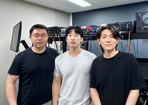
< Photo 1. Dr. Moojune Song (left) and Professor Kab-Jin Kim (right) of KAIST Department of Physics >
In simple terms, the researchers developed a special chip that synchronizes light and internal magnetic vibrations (magnons), enabling the transmission of phase information between distant magnets. They succeeded in observing and controlling interference between multiple signals in real time. This marks the first experimental evidence that magnets can serve as key components in quantum computing, serving as a pivotal step toward magnet-based quantum platforms.
The N and S poles of a magnet stem from the spin of electrons inside atoms. When many atoms align, their collective spin vibrations create a quantum particle known as a “magnon.”
Magnons are especially promising because of their nonreciprocal nature—they can carry information in only one direction, which makes them suitable for quantum noise isolation in compact quantum chips. They can also couple with both light and microwaves, enabling the potential for long-distance quantum communication over tens of kilometers.
Moreover, using special materials like antiferromagnets could allow quantum computers to operate at terahertz (THz) frequencies, far surpassing today’s hardware limitations, and possibly enabling room-temperature quantum computing without the need for bulky cryogenic equipment.
To build such a system, however, one must be able to transmit, measure, and control the phase information of magnons—the starting point and propagation of their waveforms—in real time. This had not been achieved until now.
< Figure 1. Superconducting Circuit-Based Magnon-Photon Hybrid System. (a) Schematic diagram of the device. A NbN superconducting resonator circuit fabricated on a silicon substrate is coupled with spherical YIG magnets (250 μm diameter), and magnons are generated and measured in real-time via a vertical antenna. (b) Photograph of the actual device. The distance between the two YIG spheres is 12 mm, a distance at which they cannot influence each other without the superconducting circuit. >
Professor Kim’s team used two tiny magnetic spheres made of Yttrium Iron Garnet (YIG) placed 12 mm apart with a superconducting resonator in between—similar to those used in quantum processors by Google and IBM. They input pulses into one magnet and successfully observed lossless transmission of magnon vibrations to the second magnet via the superconducting circuit.
They confirmed that from single nanosecond pulses to four microwave pulses, the magnon vibrations maintained their phase information and demonstrated predictable constructive or destructive interference in real time—known as coherent interference.
By adjusting the pulse frequencies and their intervals, the researchers could also freely control the interference patterns of magnons, effectively showing for the first time that electrical signals can be used to manipulate magnonic quantum states.
This work demonstrated that quantum gate operations using multiple pulses—a fundamental technique in quantum information processing—can be implemented using a hybrid system of magnetic materials and superconducting circuits. This opens the door for the practical use of magnet-based quantum devices.
< Figure 2. Experimental Data. (a) Measurement results of magnon-magnon band anticrossing via continuous wave measurement, showing the formation of a strong coupling hybrid system. (b) Magnon pulse exchange oscillation phenomenon between YIG spheres upon single pulse application. It can be seen that magnon information is coherently transmitted at regular time intervals through the superconducting circuit. (c,d) Magnon interference phenomenon upon dual pulse application. The magnon information state can be arbitrarily controlled by adjusting the time interval and carrier frequency between pulses. >
Professor Kab-Jin Kim stated, “This project began with a bold, even unconventional idea proposed to the Global Singularity Research Program: ‘What if we could build a quantum computer with magnets?’ The journey has been fascinating, and this study not only opens a new field of quantum spintronics, but also marks a turning point in developing high-efficiency quantum information processing devices.”
The research was co-led by postdoctoral researcher Moojune Song (KAIST), Dr. Yi Li and Dr. Valentine Novosad from Argonne National Lab, and Prof. Axel Hoffmann’s team at UIUC. The results were published in Nature Communications on April 17 and npj Spintronics on April 1, 2025.
Paper 1: Single-shot magnon interference in a magnon-superconducting-resonator hybrid circuit, Nat. Commun. 16, 3649 (2025)
DOI: https://doi.org/10.1038/s41467-025-58482-2
Paper 2: Single-shot electrical detection of short-wavelength magnon pulse transmission in a magnonic ultra-thin-film waveguide, npj Spintronics 3, 12 (2025)
DOI: https://doi.org/10.1038/s44306-025-00072-5
The research was supported by KAIST’s Global Singularity Research Initiative, the National Research Foundation of Korea (including the Mid-Career Researcher, Leading Research Center, and Quantum Information Science Human Resource Development programs), and the U.S. Department of Energy.
2025.06.12 View 1651
KAIST Turns an Unprecedented Idea into Reality: Quantum Computing with Magnets
What started as an idea under KAIST’s Global Singularity Research Project—"Can we build a quantum computer using magnets?"—has now become a scientific reality. A KAIST-led international research team has successfully demonstrated a core quantum computing technology using magnetic materials (ferromagnets) for the first time in the world.
KAIST (represented by President Kwang-Hyung Lee) announced on the 6th of May that a team led by Professor Kab-Jin Kim from the Department of Physics, in collaboration with the Argonne National Laboratory and the University of Illinois Urbana-Champaign (UIUC), has developed a “photon-magnon hybrid chip” and successfully implemented real-time, multi-pulse interference using magnetic materials—marking a global first.
< Photo 1. Dr. Moojune Song (left) and Professor Kab-Jin Kim (right) of KAIST Department of Physics >
In simple terms, the researchers developed a special chip that synchronizes light and internal magnetic vibrations (magnons), enabling the transmission of phase information between distant magnets. They succeeded in observing and controlling interference between multiple signals in real time. This marks the first experimental evidence that magnets can serve as key components in quantum computing, serving as a pivotal step toward magnet-based quantum platforms.
The N and S poles of a magnet stem from the spin of electrons inside atoms. When many atoms align, their collective spin vibrations create a quantum particle known as a “magnon.”
Magnons are especially promising because of their nonreciprocal nature—they can carry information in only one direction, which makes them suitable for quantum noise isolation in compact quantum chips. They can also couple with both light and microwaves, enabling the potential for long-distance quantum communication over tens of kilometers.
Moreover, using special materials like antiferromagnets could allow quantum computers to operate at terahertz (THz) frequencies, far surpassing today’s hardware limitations, and possibly enabling room-temperature quantum computing without the need for bulky cryogenic equipment.
To build such a system, however, one must be able to transmit, measure, and control the phase information of magnons—the starting point and propagation of their waveforms—in real time. This had not been achieved until now.
< Figure 1. Superconducting Circuit-Based Magnon-Photon Hybrid System. (a) Schematic diagram of the device. A NbN superconducting resonator circuit fabricated on a silicon substrate is coupled with spherical YIG magnets (250 μm diameter), and magnons are generated and measured in real-time via a vertical antenna. (b) Photograph of the actual device. The distance between the two YIG spheres is 12 mm, a distance at which they cannot influence each other without the superconducting circuit. >
Professor Kim’s team used two tiny magnetic spheres made of Yttrium Iron Garnet (YIG) placed 12 mm apart with a superconducting resonator in between—similar to those used in quantum processors by Google and IBM. They input pulses into one magnet and successfully observed lossless transmission of magnon vibrations to the second magnet via the superconducting circuit.
They confirmed that from single nanosecond pulses to four microwave pulses, the magnon vibrations maintained their phase information and demonstrated predictable constructive or destructive interference in real time—known as coherent interference.
By adjusting the pulse frequencies and their intervals, the researchers could also freely control the interference patterns of magnons, effectively showing for the first time that electrical signals can be used to manipulate magnonic quantum states.
This work demonstrated that quantum gate operations using multiple pulses—a fundamental technique in quantum information processing—can be implemented using a hybrid system of magnetic materials and superconducting circuits. This opens the door for the practical use of magnet-based quantum devices.
< Figure 2. Experimental Data. (a) Measurement results of magnon-magnon band anticrossing via continuous wave measurement, showing the formation of a strong coupling hybrid system. (b) Magnon pulse exchange oscillation phenomenon between YIG spheres upon single pulse application. It can be seen that magnon information is coherently transmitted at regular time intervals through the superconducting circuit. (c,d) Magnon interference phenomenon upon dual pulse application. The magnon information state can be arbitrarily controlled by adjusting the time interval and carrier frequency between pulses. >
Professor Kab-Jin Kim stated, “This project began with a bold, even unconventional idea proposed to the Global Singularity Research Program: ‘What if we could build a quantum computer with magnets?’ The journey has been fascinating, and this study not only opens a new field of quantum spintronics, but also marks a turning point in developing high-efficiency quantum information processing devices.”
The research was co-led by postdoctoral researcher Moojune Song (KAIST), Dr. Yi Li and Dr. Valentine Novosad from Argonne National Lab, and Prof. Axel Hoffmann’s team at UIUC. The results were published in Nature Communications on April 17 and npj Spintronics on April 1, 2025.
Paper 1: Single-shot magnon interference in a magnon-superconducting-resonator hybrid circuit, Nat. Commun. 16, 3649 (2025)
DOI: https://doi.org/10.1038/s41467-025-58482-2
Paper 2: Single-shot electrical detection of short-wavelength magnon pulse transmission in a magnonic ultra-thin-film waveguide, npj Spintronics 3, 12 (2025)
DOI: https://doi.org/10.1038/s44306-025-00072-5
The research was supported by KAIST’s Global Singularity Research Initiative, the National Research Foundation of Korea (including the Mid-Career Researcher, Leading Research Center, and Quantum Information Science Human Resource Development programs), and the U.S. Department of Energy.
2025.06.12 View 1651 -
 KAIST Successfully Develops High-Performance Water Electrolysis Without Platinum, Bringing Hydrogen Economy Closer
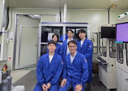
< Photo 1. (Front row, from left) Jeesoo Park (Ph.D. Candidate), Professor Hee-Tak Kim (Back row, from left) Kyunghwa Seok (Ph.D. Candidate), Dr. Gisu Doo, Euntaek Oh (Ph.D. Candidate) >
Hydrogen is gaining attention as a clean energy source that emits no carbon. Among various methods, water electrolysis, which splits water into hydrogen and oxygen using electricity, is recognized as an eco-friendly hydrogen production method. Specifically, proton exchange membrane water electrolysis (PEMWE) is considered a next-generation hydrogen production technology due to its ability to produce high-purity hydrogen at high pressure. However, existing PEMWE technology has faced limitations in commercialization due to its heavy reliance on expensive precious metal catalysts and coating materials. Korean researchers have now proposed a new solution to address these technical and economic bottlenecks.
KAIST (President Kwang Hyung Lee) announced on June 11th that a research team led by Professor Hee-Tak Kim of the Department of Chemical and Biomolecular Engineering, in a joint study with Dr. Gisu Doo of the Korea Institute of Energy Research (KIER, President Chang-keun Lee), has developed a next-generation water electrolysis technology that achieves high performance without the need for expensive platinum (Pt) coating.
The research team focused on the primary reason why 'iridium oxide (IrOx),' a highly active catalyst for water electrolysis electrodes, fails to perform optimally. They found that this is due to inefficient electron transfer and, for the first time in the world, demonstrated that performance can be maximized simply by controlling the catalyst particle size.
In this study, it was revealed that the reason iridium oxide catalysts do not exhibit excellent performance without platinum coating is due to 'electron transport resistance' that occurs at the interface between the catalyst, the ion conductor (hereinafter referred to as ionomer), and the Ti (titanium) substrate—core components inherently used together in water electrolysis electrodes.
Specifically, they identified that the 'pinch-off' phenomenon, where the electron pathway is blocked between the catalyst, ionomer, and titanium substrate, is the critical cause of reduced conductivity. The ionomer has properties close to an electron insulator, thereby hindering electron flow when it surrounds catalyst particles. Furthermore, when the ionomer comes into contact with the titanium substrate, an electron barrier forms on the surface oxide layer of the titanium substrate, significantly increasing resistance.
< Figure 1. Infographic related to electron transport resistance at the catalyst layer/diffusion layer interface >
To address this, the research team fabricated and compared catalysts of various particle sizes. Through single-cell evaluation and multiphysics simulations, they demonstrated, for the first time globally, that when iridium oxide catalyst particles with a size of 20 nanometers (nm) or larger are used, the ionomer mixed region decreases, ensuring an electron pathway and restoring conductivity.
Moreover, they successfully optimized the interfacial structure through precise design, simultaneously ensuring both reactivity and electron transport. This achievement demonstrated that the previously unavoidable trade-off between catalyst activity and conductivity can be overcome through meticulous interfacial design.
This breakthrough is expected to be a significant milestone not only for the development of high-performance catalyst materials but also for the future commercialization of proton exchange membrane water electrolysis systems that can achieve high efficiency while drastically reducing the amount of precious metals used.
Professor Hee-Tak Kim stated, "This research presents a new interface design strategy that can resolve the interfacial conductivity problem, which was a bottleneck in high-performance water electrolysis technology." He added, "By securing high performance even without expensive materials like platinum, it will be a stepping stone closer to realizing a hydrogen economy."
This research, with Jeesoo Park, a Ph.D. student from the Department of Chemical and Biomolecular Engineering at KAIST, as the first author, was published on June 7th in 'Energy & Environmental Science' (IF: 32.4, 2025), a leading international journal in the energy and environmental fields, and was recognized for its innovativeness and impact. (Paper title: On the interface electron transport problem of highly active IrOx catalysts, DOI: 10.1039/D4EE05816J).
This research was supported by the New and Renewable Energy Core Technology Development Project of the Ministry of Trade, Industry and Energy.
2025.06.11 View 1330
KAIST Successfully Develops High-Performance Water Electrolysis Without Platinum, Bringing Hydrogen Economy Closer
< Photo 1. (Front row, from left) Jeesoo Park (Ph.D. Candidate), Professor Hee-Tak Kim (Back row, from left) Kyunghwa Seok (Ph.D. Candidate), Dr. Gisu Doo, Euntaek Oh (Ph.D. Candidate) >
Hydrogen is gaining attention as a clean energy source that emits no carbon. Among various methods, water electrolysis, which splits water into hydrogen and oxygen using electricity, is recognized as an eco-friendly hydrogen production method. Specifically, proton exchange membrane water electrolysis (PEMWE) is considered a next-generation hydrogen production technology due to its ability to produce high-purity hydrogen at high pressure. However, existing PEMWE technology has faced limitations in commercialization due to its heavy reliance on expensive precious metal catalysts and coating materials. Korean researchers have now proposed a new solution to address these technical and economic bottlenecks.
KAIST (President Kwang Hyung Lee) announced on June 11th that a research team led by Professor Hee-Tak Kim of the Department of Chemical and Biomolecular Engineering, in a joint study with Dr. Gisu Doo of the Korea Institute of Energy Research (KIER, President Chang-keun Lee), has developed a next-generation water electrolysis technology that achieves high performance without the need for expensive platinum (Pt) coating.
The research team focused on the primary reason why 'iridium oxide (IrOx),' a highly active catalyst for water electrolysis electrodes, fails to perform optimally. They found that this is due to inefficient electron transfer and, for the first time in the world, demonstrated that performance can be maximized simply by controlling the catalyst particle size.
In this study, it was revealed that the reason iridium oxide catalysts do not exhibit excellent performance without platinum coating is due to 'electron transport resistance' that occurs at the interface between the catalyst, the ion conductor (hereinafter referred to as ionomer), and the Ti (titanium) substrate—core components inherently used together in water electrolysis electrodes.
Specifically, they identified that the 'pinch-off' phenomenon, where the electron pathway is blocked between the catalyst, ionomer, and titanium substrate, is the critical cause of reduced conductivity. The ionomer has properties close to an electron insulator, thereby hindering electron flow when it surrounds catalyst particles. Furthermore, when the ionomer comes into contact with the titanium substrate, an electron barrier forms on the surface oxide layer of the titanium substrate, significantly increasing resistance.
< Figure 1. Infographic related to electron transport resistance at the catalyst layer/diffusion layer interface >
To address this, the research team fabricated and compared catalysts of various particle sizes. Through single-cell evaluation and multiphysics simulations, they demonstrated, for the first time globally, that when iridium oxide catalyst particles with a size of 20 nanometers (nm) or larger are used, the ionomer mixed region decreases, ensuring an electron pathway and restoring conductivity.
Moreover, they successfully optimized the interfacial structure through precise design, simultaneously ensuring both reactivity and electron transport. This achievement demonstrated that the previously unavoidable trade-off between catalyst activity and conductivity can be overcome through meticulous interfacial design.
This breakthrough is expected to be a significant milestone not only for the development of high-performance catalyst materials but also for the future commercialization of proton exchange membrane water electrolysis systems that can achieve high efficiency while drastically reducing the amount of precious metals used.
Professor Hee-Tak Kim stated, "This research presents a new interface design strategy that can resolve the interfacial conductivity problem, which was a bottleneck in high-performance water electrolysis technology." He added, "By securing high performance even without expensive materials like platinum, it will be a stepping stone closer to realizing a hydrogen economy."
This research, with Jeesoo Park, a Ph.D. student from the Department of Chemical and Biomolecular Engineering at KAIST, as the first author, was published on June 7th in 'Energy & Environmental Science' (IF: 32.4, 2025), a leading international journal in the energy and environmental fields, and was recognized for its innovativeness and impact. (Paper title: On the interface electron transport problem of highly active IrOx catalysts, DOI: 10.1039/D4EE05816J).
This research was supported by the New and Renewable Energy Core Technology Development Project of the Ministry of Trade, Industry and Energy.
2025.06.11 View 1330 -
 KAIST Research Team Develops Electronic Ink for Room-Temperature Printing of High-Resolution, Variable-Stiffness Electronics
A team of researchers from KAIST and Seoul National University has developed a groundbreaking electronic ink that enables room-temperature printing of variable-stiffness circuits capable of switching between rigid and soft modes. This advancement marks a significant leap toward next-generation wearable, implantable, and robotic devices.
< Photo 1. (From left) Professor Jae-Woong Jeong and PhD candidate Simok Lee of the School of Electrical Engineering, (in separate bubbles, from left) Professor Gun-Hee Lee of Pusan National University, Professor Seongjun Park of Seoul National University, Professor Steve Park of the Department of Materials Science and Engineering>
Variable-stiffness electronics are at the forefront of adaptive technology, offering the ability for a single device to transition between rigid and soft modes depending on its use case. Gallium, a metal known for its high rigidity contrast between solid and liquid states, is a promising candidate for such applications. However, its use has been hindered by challenges including high surface tension, low viscosity, and undesirable phase transitions during manufacturing.
On June 4th, a research team led by Professor Jae-Woong Jeong from the School of Electrical Engineering at KAIST, Professor Seongjun Park from the Digital Healthcare Major at Seoul National University, and Professor Steve Park from the Department of Materials Science and Engineering at KAIST introduced a novel liquid metal electronic ink. This ink allows for micro-scale circuit printing – thinner than a human hair – at room temperature, with the ability to reversibly switch between rigid and soft modes depending on temperature.
The new ink combines printable viscosity with excellent electrical conductivity, enabling the creation of complex, high-resolution multilayer circuits comparable to commercial printed circuit boards (PCBs). These circuits can dynamically change stiffness in response to temperature, presenting new opportunities for multifunctional electronics, medical technologies, and robotics.
Conventional electronics typically have fixed form factors – either rigid for durability or soft for wearability. Rigid devices like smartphones and laptops offer robust performance but are uncomfortable when worn, while soft electronics are more comfortable but lack precise handling. As demand grows for devices that can adapt their stiffness to context, variable-stiffness electronics are becoming increasingly important.
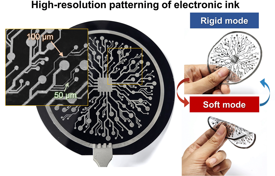
< Figure 1. Fabrication process of stable, high-viscosity electronic ink by dispersing micro-sized gallium particles in a polymer matrix (left). High-resolution large-area circuit printing process through pH-controlled chemical sintering (right). >
To address this challenge, the researchers focused on gallium, which melts just below body temperature. Solid gallium is quite stiff, while its liquid form is fluid and soft. Despite its potential, gallium’s use in electronic printing has been limited by its high surface tension and instability when melted.
To overcome these issues, the team developed a pH-controlled liquid metal ink printing process. By dispersing micro-sized gallium particles into a hydrophilic polyurethane matrix using a neutral solvent (dimethyl sulfoxide, or DMSO), they created a stable, high-viscosity ink suitable for precision printing. During post-print heating, the DMSO decomposes to form an acidic environment, which removes the oxide layer on the gallium particles. This triggers the particles to coalesce into electrically conductive networks with tunable mechanical properties.
The resulting printed circuits exhibit fine feature sizes (~50 μm), high conductivity (2.27 × 10⁶ S/m), and a stiffness modulation ratio of up to 1,465 – allowing the material to shift from plastic-like rigidity to rubber-like softness. Furthermore, the ink is compatible with conventional printing techniques such as screen printing and dip coating, supporting large-area and 3D device fabrication.
< Figure 2. Key features of the electronic ink. (i) High-resolution printing and multilayer integration capability. (ii) Batch fabrication capability through large-area screen printing. (iii) Complex three-dimensional structure printing capability through dip coating. (iv) Excellent electrical conductivity and stiffness control capability.>
The team demonstrated this technology by developing a multi-functional device that operates as a rigid portable electronic under normal conditions but transforms into a soft wearable healthcare device when attached to the body. They also created a neural probe that remains stiff during surgical insertion for accurate positioning but softens once inside brain tissue to reduce inflammation – highlighting its potential for biomedical implants.
< Figure 3. Variable stiffness wearable electronics with high-resolution circuits and multilayer structure comparable to commercial printed circuit boards (PCBs). Functions as a rigid portable electronic device at room temperature, then transforms into a wearable healthcare device by softening at body temperature upon skin contact.>
“The core achievement of this research lies in overcoming the longstanding challenges of liquid metal printing through our innovative technology,” said Professor Jeong. “By controlling the ink’s acidity, we were able to electrically and mechanically connect printed gallium particles, enabling the room-temperature fabrication of high-resolution, large-area circuits with tunable stiffness. This opens up new possibilities for future personal electronics, medical devices, and robotics.”
< Figure 4. Body-temperature softening neural probe implemented by coating electronic ink on an optical waveguide structure. (Left) Remains rigid during surgery for precise manipulation and brain insertion, then softens after implantation to minimize mechanical stress on the brain and greatly enhance biocompatibility. (Right) >
This research was published in Science Advances under the title, “Phase-Change Metal Ink with pH-Controlled Chemical Sintering for Versatile and Scalable Fabrication of Variable Stiffness Electronics.” The work was supported by the National Research Foundation of Korea, the Boston-Korea Project, and the BK21 FOUR Program.
2025.06.04 View 1683
KAIST Research Team Develops Electronic Ink for Room-Temperature Printing of High-Resolution, Variable-Stiffness Electronics
A team of researchers from KAIST and Seoul National University has developed a groundbreaking electronic ink that enables room-temperature printing of variable-stiffness circuits capable of switching between rigid and soft modes. This advancement marks a significant leap toward next-generation wearable, implantable, and robotic devices.
< Photo 1. (From left) Professor Jae-Woong Jeong and PhD candidate Simok Lee of the School of Electrical Engineering, (in separate bubbles, from left) Professor Gun-Hee Lee of Pusan National University, Professor Seongjun Park of Seoul National University, Professor Steve Park of the Department of Materials Science and Engineering>
Variable-stiffness electronics are at the forefront of adaptive technology, offering the ability for a single device to transition between rigid and soft modes depending on its use case. Gallium, a metal known for its high rigidity contrast between solid and liquid states, is a promising candidate for such applications. However, its use has been hindered by challenges including high surface tension, low viscosity, and undesirable phase transitions during manufacturing.
On June 4th, a research team led by Professor Jae-Woong Jeong from the School of Electrical Engineering at KAIST, Professor Seongjun Park from the Digital Healthcare Major at Seoul National University, and Professor Steve Park from the Department of Materials Science and Engineering at KAIST introduced a novel liquid metal electronic ink. This ink allows for micro-scale circuit printing – thinner than a human hair – at room temperature, with the ability to reversibly switch between rigid and soft modes depending on temperature.
The new ink combines printable viscosity with excellent electrical conductivity, enabling the creation of complex, high-resolution multilayer circuits comparable to commercial printed circuit boards (PCBs). These circuits can dynamically change stiffness in response to temperature, presenting new opportunities for multifunctional electronics, medical technologies, and robotics.
Conventional electronics typically have fixed form factors – either rigid for durability or soft for wearability. Rigid devices like smartphones and laptops offer robust performance but are uncomfortable when worn, while soft electronics are more comfortable but lack precise handling. As demand grows for devices that can adapt their stiffness to context, variable-stiffness electronics are becoming increasingly important.
< Figure 1. Fabrication process of stable, high-viscosity electronic ink by dispersing micro-sized gallium particles in a polymer matrix (left). High-resolution large-area circuit printing process through pH-controlled chemical sintering (right). >
To address this challenge, the researchers focused on gallium, which melts just below body temperature. Solid gallium is quite stiff, while its liquid form is fluid and soft. Despite its potential, gallium’s use in electronic printing has been limited by its high surface tension and instability when melted.
To overcome these issues, the team developed a pH-controlled liquid metal ink printing process. By dispersing micro-sized gallium particles into a hydrophilic polyurethane matrix using a neutral solvent (dimethyl sulfoxide, or DMSO), they created a stable, high-viscosity ink suitable for precision printing. During post-print heating, the DMSO decomposes to form an acidic environment, which removes the oxide layer on the gallium particles. This triggers the particles to coalesce into electrically conductive networks with tunable mechanical properties.
The resulting printed circuits exhibit fine feature sizes (~50 μm), high conductivity (2.27 × 10⁶ S/m), and a stiffness modulation ratio of up to 1,465 – allowing the material to shift from plastic-like rigidity to rubber-like softness. Furthermore, the ink is compatible with conventional printing techniques such as screen printing and dip coating, supporting large-area and 3D device fabrication.
< Figure 2. Key features of the electronic ink. (i) High-resolution printing and multilayer integration capability. (ii) Batch fabrication capability through large-area screen printing. (iii) Complex three-dimensional structure printing capability through dip coating. (iv) Excellent electrical conductivity and stiffness control capability.>
The team demonstrated this technology by developing a multi-functional device that operates as a rigid portable electronic under normal conditions but transforms into a soft wearable healthcare device when attached to the body. They also created a neural probe that remains stiff during surgical insertion for accurate positioning but softens once inside brain tissue to reduce inflammation – highlighting its potential for biomedical implants.
< Figure 3. Variable stiffness wearable electronics with high-resolution circuits and multilayer structure comparable to commercial printed circuit boards (PCBs). Functions as a rigid portable electronic device at room temperature, then transforms into a wearable healthcare device by softening at body temperature upon skin contact.>
“The core achievement of this research lies in overcoming the longstanding challenges of liquid metal printing through our innovative technology,” said Professor Jeong. “By controlling the ink’s acidity, we were able to electrically and mechanically connect printed gallium particles, enabling the room-temperature fabrication of high-resolution, large-area circuits with tunable stiffness. This opens up new possibilities for future personal electronics, medical devices, and robotics.”
< Figure 4. Body-temperature softening neural probe implemented by coating electronic ink on an optical waveguide structure. (Left) Remains rigid during surgery for precise manipulation and brain insertion, then softens after implantation to minimize mechanical stress on the brain and greatly enhance biocompatibility. (Right) >
This research was published in Science Advances under the title, “Phase-Change Metal Ink with pH-Controlled Chemical Sintering for Versatile and Scalable Fabrication of Variable Stiffness Electronics.” The work was supported by the National Research Foundation of Korea, the Boston-Korea Project, and the BK21 FOUR Program.
2025.06.04 View 1683 -
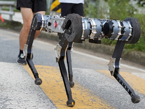 RAIBO Runs over Walls with Feline Agility... Ready for Effortless Search over Mountaineous and Rough Terrains
< Photo 1. Research Team Photo (Professor Jemin Hwangbo, second from right in the front row) >
KAIST's quadrupedal robot, RAIBO, can now move at high speed across discontinuous and complex terrains such as stairs, gaps, walls, and debris. It has demonstrated its ability to run on vertical walls, leap over 1.3-meter-wide gaps, sprint at approximately 14.4 km/h over stepping stones, and move quickly and nimbly on terrain combining 30° slopes, stairs, and stepping stones. RAIBO is expected to be deployed soon for practical missions such as disaster site exploration and mountain searches.
Professor Jemin Hwangbo's research team in the Department of Mechanical Engineering at our university announced on June 3rd that they have developed a quadrupedal robot navigation framework capable of high-speed locomotion at 14.4 km/h (4m/s) even on discontinuous and complex terrains such as walls, stairs, and stepping stones.
The research team developed a quadrupedal navigation system that enables the robot to reach its target destination quickly and safely in complex and discontinuous terrain.
To achieve this, they approached the problem by breaking it down into two stages: first, developing a planner for planning foothold positions, and second, developing a tracker to accurately follow the planned foothold positions.
First, the planner module quickly searches for physically feasible foothold positions using a sampling-based optimization method with neural network-based heuristics and verifies the optimal path through simulation rollouts.
While existing methods considered various factors such as contact timing and robot posture in addition to foothold positions, this research significantly reduced computational complexity by setting only foothold positions as the search space. Furthermore, inspired by the walking method of cats, the introduction of a structure where the hind feet step on the same spots as the front feet further significantly reduced computational complexity.
< Figure 1. High-speed navigation across various discontinuous terrains >
Second, the tracker module is trained to accurately step on planned positions, and tracking training is conducted through a generative model that competes in environments of appropriate difficulty.
The tracker is trained through reinforcement learning to accurately step on planned plots, and during this process, a generative model called the 'map generator' provides the target distribution.
This generative model is trained simultaneously and adversarially with the tracker to allow the tracker to progressively adapt to more challenging difficulties. Subsequently, a sampling-based planner was designed to generate feasible foothold plans that can reflect the characteristics and performance of the trained tracker.
This hierarchical structure showed superior performance in both planning speed and stability compared to existing techniques, and experiments proved its high-speed locomotion capabilities across various obstacles and discontinuous terrains, as well as its general applicability to unseen terrains.
Professor Jemin Hwangbo stated, "We approached the problem of high-speed navigation in discontinuous terrain, which previously required a significantly large amount of computation, from the simple perspective of how to select the footprint positions. Inspired by the placements of cat's paw, allowing the hind feet to step where the front feet stepped drastically reduced computation. We expect this to significantly expand the range of discontinuous terrain that walking robots can overcome and enable them to traverse it at high speeds, contributing to the robot's ability to perform practical missions such as disaster site exploration and mountain searches."
This research achievement was published in the May 2025 issue of the international journal Science Robotics.
Paper Title: High-speed control and navigation for quadrupedal robots on complex and discrete terrain, (https://www.science.org/doi/10.1126/scirobotics.ads6192)YouTube Link: https://youtu.be/EZbM594T3c4?si=kfxLF2XnVUvYVIyk
2025.06.04 View 1984
RAIBO Runs over Walls with Feline Agility... Ready for Effortless Search over Mountaineous and Rough Terrains
< Photo 1. Research Team Photo (Professor Jemin Hwangbo, second from right in the front row) >
KAIST's quadrupedal robot, RAIBO, can now move at high speed across discontinuous and complex terrains such as stairs, gaps, walls, and debris. It has demonstrated its ability to run on vertical walls, leap over 1.3-meter-wide gaps, sprint at approximately 14.4 km/h over stepping stones, and move quickly and nimbly on terrain combining 30° slopes, stairs, and stepping stones. RAIBO is expected to be deployed soon for practical missions such as disaster site exploration and mountain searches.
Professor Jemin Hwangbo's research team in the Department of Mechanical Engineering at our university announced on June 3rd that they have developed a quadrupedal robot navigation framework capable of high-speed locomotion at 14.4 km/h (4m/s) even on discontinuous and complex terrains such as walls, stairs, and stepping stones.
The research team developed a quadrupedal navigation system that enables the robot to reach its target destination quickly and safely in complex and discontinuous terrain.
To achieve this, they approached the problem by breaking it down into two stages: first, developing a planner for planning foothold positions, and second, developing a tracker to accurately follow the planned foothold positions.
First, the planner module quickly searches for physically feasible foothold positions using a sampling-based optimization method with neural network-based heuristics and verifies the optimal path through simulation rollouts.
While existing methods considered various factors such as contact timing and robot posture in addition to foothold positions, this research significantly reduced computational complexity by setting only foothold positions as the search space. Furthermore, inspired by the walking method of cats, the introduction of a structure where the hind feet step on the same spots as the front feet further significantly reduced computational complexity.
< Figure 1. High-speed navigation across various discontinuous terrains >
Second, the tracker module is trained to accurately step on planned positions, and tracking training is conducted through a generative model that competes in environments of appropriate difficulty.
The tracker is trained through reinforcement learning to accurately step on planned plots, and during this process, a generative model called the 'map generator' provides the target distribution.
This generative model is trained simultaneously and adversarially with the tracker to allow the tracker to progressively adapt to more challenging difficulties. Subsequently, a sampling-based planner was designed to generate feasible foothold plans that can reflect the characteristics and performance of the trained tracker.
This hierarchical structure showed superior performance in both planning speed and stability compared to existing techniques, and experiments proved its high-speed locomotion capabilities across various obstacles and discontinuous terrains, as well as its general applicability to unseen terrains.
Professor Jemin Hwangbo stated, "We approached the problem of high-speed navigation in discontinuous terrain, which previously required a significantly large amount of computation, from the simple perspective of how to select the footprint positions. Inspired by the placements of cat's paw, allowing the hind feet to step where the front feet stepped drastically reduced computation. We expect this to significantly expand the range of discontinuous terrain that walking robots can overcome and enable them to traverse it at high speeds, contributing to the robot's ability to perform practical missions such as disaster site exploration and mountain searches."
This research achievement was published in the May 2025 issue of the international journal Science Robotics.
Paper Title: High-speed control and navigation for quadrupedal robots on complex and discrete terrain, (https://www.science.org/doi/10.1126/scirobotics.ads6192)YouTube Link: https://youtu.be/EZbM594T3c4?si=kfxLF2XnVUvYVIyk
2025.06.04 View 1984 -
 New 'Science Hall of Fame' Opens in Vision Hall, Highlighting Achievements of Modern and Contemporary Scientists
A portion of the existing exhibition space in the 'KAIST Vision Hall,' located at our university's main campus in Daejeon, has been reorganized as the 'KAIST Science Hall of Fame' and opened to the public.
Opened in March 2018 on the first floor of the Academic and Cultural Complex, the KAIST Vision Hall is a historical exhibition hall that has showcased KAIST's major history and research achievements from its establishment to the present. In particular, various materials that formed the foundation of KAIST's establishment are displayed, including the 'Survey Report on the Establishment of the Korea Advanced Institute of Science (also known as the Terman Report),' which was prepared through a due diligence conducted by the U.S. Agency for International Development (USAID) in 1970.
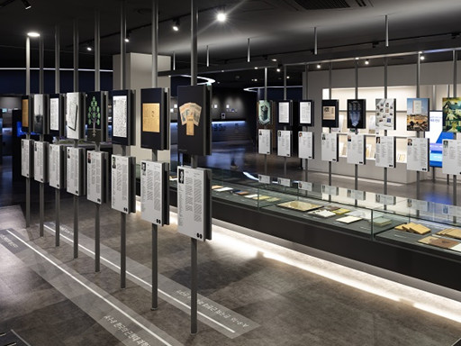
< Overall View of the Science Hall of Fame within Vision Hall >
Through this exhibition reorganization, Vision Hall has expanded its scope to not only trace KAIST's journey but also highlight prominent scientists who have made significant achievements across the entire Korean science and technology community.
The newly revamped 'KAIST Science Hall of Fame' consists of two main sections. The first section introduces modern and contemporary scientists who dedicated themselves to research even under challenging political and social conditions, such as during the Japanese colonial period. The second section focuses on the research achievements and international cooperation cases accomplished by KAIST researchers, built upon the efforts of these pioneering scientists.
< Overall View of the Science Hall of Fame within Vision Hall >
Professor Geun-bae Kim of the Department of Science at Jeonbuk National University, who advised on the exhibition reorganization, expressed his feelings, saying, "I am delighted that my efforts in researching modern and contemporary science history and the socio-history of science have been of even a small help in this reorganization of the KAIST Vision Hall exhibition."
Seung-Mok Son, Team Leader of the KAIST Arts & Culture Center, who oversaw the planning and operation of the exhibition space, stated, "This exhibition is a special composition that unpacks the history of Korean science through a human-centered narrative. We expect visitors to gain deep inspiration through the lives and visions of our scientific predecessors."
KAIST President Kwang-Hyung Lee remarked, "Just as a tall tree has deep roots, KAIST's ideals and achievements are rooted in the dedication of our scientific predecessors. We have newly established the Hall of Science and Technology Figures to honor their spirit and pass it on to future generations."
< Overall View of the Science Hall of Fame within Vision Hall >
Vision Hall operates from 10:00 AM to 5:00 PM on weekdays and is open to the general public as well as KAIST members free of charge. The newly established 'KAIST Science Hall of Fame' features actual exhibits such as research notes, historical photographs, degrees, newspaper articles, and handwritten manuscripts of pioneering scientists. Public viewing became available in the afternoon of the same day, following the opening ceremony held in the morning of the 2nd. More detailed information can be found on the official Vision Hall website: https://visionhall.kaist.ac.kr/.
※ Related Video: KAIST Science Hall of Fame Video at YouTube Channel "KAIST art museum" https://youtu.be/TlC93xMRfxU?si=3Lf0fzcWU3q1spKf
2025.06.02 View 113
New 'Science Hall of Fame' Opens in Vision Hall, Highlighting Achievements of Modern and Contemporary Scientists
A portion of the existing exhibition space in the 'KAIST Vision Hall,' located at our university's main campus in Daejeon, has been reorganized as the 'KAIST Science Hall of Fame' and opened to the public.
Opened in March 2018 on the first floor of the Academic and Cultural Complex, the KAIST Vision Hall is a historical exhibition hall that has showcased KAIST's major history and research achievements from its establishment to the present. In particular, various materials that formed the foundation of KAIST's establishment are displayed, including the 'Survey Report on the Establishment of the Korea Advanced Institute of Science (also known as the Terman Report),' which was prepared through a due diligence conducted by the U.S. Agency for International Development (USAID) in 1970.
< Overall View of the Science Hall of Fame within Vision Hall >
Through this exhibition reorganization, Vision Hall has expanded its scope to not only trace KAIST's journey but also highlight prominent scientists who have made significant achievements across the entire Korean science and technology community.
The newly revamped 'KAIST Science Hall of Fame' consists of two main sections. The first section introduces modern and contemporary scientists who dedicated themselves to research even under challenging political and social conditions, such as during the Japanese colonial period. The second section focuses on the research achievements and international cooperation cases accomplished by KAIST researchers, built upon the efforts of these pioneering scientists.
< Overall View of the Science Hall of Fame within Vision Hall >
Professor Geun-bae Kim of the Department of Science at Jeonbuk National University, who advised on the exhibition reorganization, expressed his feelings, saying, "I am delighted that my efforts in researching modern and contemporary science history and the socio-history of science have been of even a small help in this reorganization of the KAIST Vision Hall exhibition."
Seung-Mok Son, Team Leader of the KAIST Arts & Culture Center, who oversaw the planning and operation of the exhibition space, stated, "This exhibition is a special composition that unpacks the history of Korean science through a human-centered narrative. We expect visitors to gain deep inspiration through the lives and visions of our scientific predecessors."
KAIST President Kwang-Hyung Lee remarked, "Just as a tall tree has deep roots, KAIST's ideals and achievements are rooted in the dedication of our scientific predecessors. We have newly established the Hall of Science and Technology Figures to honor their spirit and pass it on to future generations."
< Overall View of the Science Hall of Fame within Vision Hall >
Vision Hall operates from 10:00 AM to 5:00 PM on weekdays and is open to the general public as well as KAIST members free of charge. The newly established 'KAIST Science Hall of Fame' features actual exhibits such as research notes, historical photographs, degrees, newspaper articles, and handwritten manuscripts of pioneering scientists. Public viewing became available in the afternoon of the same day, following the opening ceremony held in the morning of the 2nd. More detailed information can be found on the official Vision Hall website: https://visionhall.kaist.ac.kr/.
※ Related Video: KAIST Science Hall of Fame Video at YouTube Channel "KAIST art museum" https://youtu.be/TlC93xMRfxU?si=3Lf0fzcWU3q1spKf
2025.06.02 View 113 -
 KAIST to Develop a Korean-style ChatGPT Platform Specifically Geared Toward Medical Diagnosis and Drug Discovery
On May 23rd, KAIST (President Kwang-Hyung Lee) announced that its Digital Bio-Health AI Research Center (Director: Professor JongChul Ye of KAIST Kim Jaechul Graduate School of AI) has been selected for the Ministry of Science and ICT's 'AI Top-Tier Young Researcher Support Program (AI Star Fellowship Project).' With a total investment of ₩11.5 billion from May 2025 to December 2030, the center will embark on the full-scale development of AI technology and a platform capable of independently inferring and determining the kinds of diseases, and discovering new drugs.
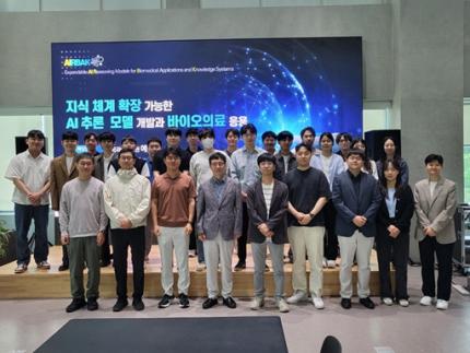
< Photo. On May 20th, a kick-off meeting for the AI Star Fellowship Project was held at KAIST Kim Jaechul Graduate School of AI’s Yangjae Research Center with the KAIST research team and participating organizations of Samsung Medical Center, NAVER Cloud, and HITS. [From left to right in the front row] Professor Jaegul Joo (KAIST), Professor Yoonjae Choi (KAIST), Professor Woo Youn Kim (KAIST/HITS), Professor JongChul Ye (KAIST), Professor Sungsoo Ahn (KAIST), Dr. Haanju Yoo (NAVER Cloud), Yoonho Lee (KAIST), HyeYoon Moon (Samsung Medical Center), Dr. Su Min Kim (Samsung Medical Center) >
This project aims to foster an innovative AI research ecosystem centered on young researchers and develop an inferential AI agent that can utilize and automatically expand specialized knowledge systems in the bio and medical fields.
Professor JongChul Ye of the Kim Jaechul Graduate School of AI will serve as the lead researcher, with young researchers from KAIST including Professors Yoonjae Choi, Kimin Lee, Sungsoo Ahn, and Chanyoung Park, along with mid-career researchers like Professors Jaegul Joo and Woo Youn Kim, jointly undertaking the project. They will collaborate with various laboratories within KAIST to conduct comprehensive research covering the entire cycle from the theoretical foundations of AI inference to its practical application.
Specifically, the main goals include: - Building high-performance inference models that integrate diverse medical knowledge systems to enhance the precision and reliability of diagnosis and treatment. - Developing a convergence inference platform that efficiently combines symbol-based inference with neural network models. - Securing AI technology for new drug development and biomarker discovery based on 'cell ontology.'
Furthermore, through close collaboration with industry and medical institutions such as Samsung Medical Center, NAVER Cloud, and HITS Co., Ltd., the project aims to achieve: - Clinical diagnostic AI utilizing medical knowledge systems. - AI-based molecular target exploration for new drug development. - Commercialization of an extendible AI inference platform.
Professor JongChul Ye, Director of KAIST's Digital Bio-Health AI Research Center, stated, "At a time when competition in AI inference model development is intensifying, it is a great honor for KAIST to lead the development of AI technology specialized in the bio and medical fields with world-class young researchers." He added, "We will do our best to ensure that the participating young researchers reach a world-leading level in terms of research achievements after the completion of this seven-year project starting in 2025."
The AI Star Fellowship is a newly established program where post-doctoral researchers and faculty members within seven years of appointment participate as project leaders (PLs) to independently lead research. Multiple laboratories within a university and demand-side companies form a consortium to operate the program.
Through this initiative, KAIST plans to nurture bio-medical convergence AI talent and simultaneously promote the commercialization of core technologies in collaboration with Samsung Medical Center, NAVER Cloud, and HITS.
2025.05.26 View 2798
KAIST to Develop a Korean-style ChatGPT Platform Specifically Geared Toward Medical Diagnosis and Drug Discovery
On May 23rd, KAIST (President Kwang-Hyung Lee) announced that its Digital Bio-Health AI Research Center (Director: Professor JongChul Ye of KAIST Kim Jaechul Graduate School of AI) has been selected for the Ministry of Science and ICT's 'AI Top-Tier Young Researcher Support Program (AI Star Fellowship Project).' With a total investment of ₩11.5 billion from May 2025 to December 2030, the center will embark on the full-scale development of AI technology and a platform capable of independently inferring and determining the kinds of diseases, and discovering new drugs.
< Photo. On May 20th, a kick-off meeting for the AI Star Fellowship Project was held at KAIST Kim Jaechul Graduate School of AI’s Yangjae Research Center with the KAIST research team and participating organizations of Samsung Medical Center, NAVER Cloud, and HITS. [From left to right in the front row] Professor Jaegul Joo (KAIST), Professor Yoonjae Choi (KAIST), Professor Woo Youn Kim (KAIST/HITS), Professor JongChul Ye (KAIST), Professor Sungsoo Ahn (KAIST), Dr. Haanju Yoo (NAVER Cloud), Yoonho Lee (KAIST), HyeYoon Moon (Samsung Medical Center), Dr. Su Min Kim (Samsung Medical Center) >
This project aims to foster an innovative AI research ecosystem centered on young researchers and develop an inferential AI agent that can utilize and automatically expand specialized knowledge systems in the bio and medical fields.
Professor JongChul Ye of the Kim Jaechul Graduate School of AI will serve as the lead researcher, with young researchers from KAIST including Professors Yoonjae Choi, Kimin Lee, Sungsoo Ahn, and Chanyoung Park, along with mid-career researchers like Professors Jaegul Joo and Woo Youn Kim, jointly undertaking the project. They will collaborate with various laboratories within KAIST to conduct comprehensive research covering the entire cycle from the theoretical foundations of AI inference to its practical application.
Specifically, the main goals include: - Building high-performance inference models that integrate diverse medical knowledge systems to enhance the precision and reliability of diagnosis and treatment. - Developing a convergence inference platform that efficiently combines symbol-based inference with neural network models. - Securing AI technology for new drug development and biomarker discovery based on 'cell ontology.'
Furthermore, through close collaboration with industry and medical institutions such as Samsung Medical Center, NAVER Cloud, and HITS Co., Ltd., the project aims to achieve: - Clinical diagnostic AI utilizing medical knowledge systems. - AI-based molecular target exploration for new drug development. - Commercialization of an extendible AI inference platform.
Professor JongChul Ye, Director of KAIST's Digital Bio-Health AI Research Center, stated, "At a time when competition in AI inference model development is intensifying, it is a great honor for KAIST to lead the development of AI technology specialized in the bio and medical fields with world-class young researchers." He added, "We will do our best to ensure that the participating young researchers reach a world-leading level in terms of research achievements after the completion of this seven-year project starting in 2025."
The AI Star Fellowship is a newly established program where post-doctoral researchers and faculty members within seven years of appointment participate as project leaders (PLs) to independently lead research. Multiple laboratories within a university and demand-side companies form a consortium to operate the program.
Through this initiative, KAIST plans to nurture bio-medical convergence AI talent and simultaneously promote the commercialization of core technologies in collaboration with Samsung Medical Center, NAVER Cloud, and HITS.
2025.05.26 View 2798 -
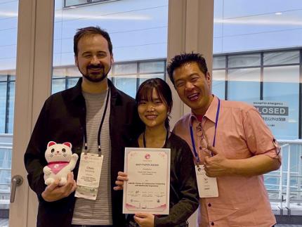 KAIST & CMU Unveils Amuse, a Songwriting AI-Collaborator to Help Create Music
Wouldn't it be great if music creators had someone to brainstorm with, help them when they're stuck, and explore different musical directions together? Researchers of KAIST and Carnegie Mellon University (CMU) have developed AI technology similar to a fellow songwriter who helps create music.
KAIST (President Kwang-Hyung Lee) has developed an AI-based music creation support system, Amuse, by a research team led by Professor Sung-Ju Lee of the School of Electrical Engineering in collaboration with CMU. The research was presented at the ACM Conference on Human Factors in Computing Systems (CHI), one of the world’s top conferences in human-computer interaction, held in Yokohama, Japan from April 26 to May 1. It received the Best Paper Award, given to only the top 1% of all submissions.
< (From left) Professor Chris Donahue of Carnegie Mellon University, Ph.D. Student Yewon Kim and Professor Sung-Ju Lee of the School of Electrical Engineering >
The system developed by Professor Sung-Ju Lee’s research team, Amuse, is an AI-based system that converts various forms of inspiration such as text, images, and audio into harmonic structures (chord progressions) to support composition.
For example, if a user inputs a phrase, image, or sound clip such as “memories of a warm summer beach”, Amuse automatically generates and suggests chord progressions that match the inspiration.
Unlike existing generative AI, Amuse is differentiated in that it respects the user's creative flow and naturally induces creative exploration through an interactive method that allows flexible integration and modification of AI suggestions.
The core technology of the Amuse system is a generation method that blends two approaches: a large language model creates music code based on the user's prompt and inspiration, while another AI model, trained on real music data, filters out awkward or unnatural results using rejection sampling.
< Figure 1. Amuse system configuration. After extracting music keywords from user input, a large language model-based code progression is generated and refined through rejection sampling (left). Code extraction from audio input is also possible (right). The bottom is an example visualizing the chord structure of the generated code. >
The research team conducted a user study targeting actual musicians and evaluated that Amuse has high potential as a creative companion, or a Co-Creative AI, a concept in which people and AI collaborate, rather than having a generative AI simply put together a song.
The paper, in which a Ph.D. student Yewon Kim and Professor Sung-Ju Lee of KAIST School of Electrical and Electronic Engineering and Carnegie Mellon University Professor Chris Donahue participated, demonstrated the potential of creative AI system design in both academia and industry. ※ Paper title: Amuse: Human-AI Collaborative Songwriting with Multimodal Inspirations DOI: https://doi.org/10.1145/3706598.3713818
※ Research demo video: https://youtu.be/udilkRSnftI?si=FNXccC9EjxHOCrm1
※ Research homepage: https://nmsl.kaist.ac.kr/projects/amuse/
Professor Sung-Ju Lee said, “Recent generative AI technology has raised concerns in that it directly imitates copyrighted content, thereby violating the copyright of the creator, or generating results one-way regardless of the creator’s intention. Accordingly, the research team was aware of this trend, paid attention to what the creator actually needs, and focused on designing an AI system centered on the creator.”
He continued, “Amuse is an attempt to explore the possibility of collaboration with AI while maintaining the initiative of the creator, and is expected to be a starting point for suggesting a more creator-friendly direction in the development of music creation tools and generative AI systems in the future.”
This research was conducted with the support of the National Research Foundation of Korea with funding from the government (Ministry of Science and ICT). (RS-2024-00337007)
2025.05.07 View 4403
KAIST & CMU Unveils Amuse, a Songwriting AI-Collaborator to Help Create Music
Wouldn't it be great if music creators had someone to brainstorm with, help them when they're stuck, and explore different musical directions together? Researchers of KAIST and Carnegie Mellon University (CMU) have developed AI technology similar to a fellow songwriter who helps create music.
KAIST (President Kwang-Hyung Lee) has developed an AI-based music creation support system, Amuse, by a research team led by Professor Sung-Ju Lee of the School of Electrical Engineering in collaboration with CMU. The research was presented at the ACM Conference on Human Factors in Computing Systems (CHI), one of the world’s top conferences in human-computer interaction, held in Yokohama, Japan from April 26 to May 1. It received the Best Paper Award, given to only the top 1% of all submissions.
< (From left) Professor Chris Donahue of Carnegie Mellon University, Ph.D. Student Yewon Kim and Professor Sung-Ju Lee of the School of Electrical Engineering >
The system developed by Professor Sung-Ju Lee’s research team, Amuse, is an AI-based system that converts various forms of inspiration such as text, images, and audio into harmonic structures (chord progressions) to support composition.
For example, if a user inputs a phrase, image, or sound clip such as “memories of a warm summer beach”, Amuse automatically generates and suggests chord progressions that match the inspiration.
Unlike existing generative AI, Amuse is differentiated in that it respects the user's creative flow and naturally induces creative exploration through an interactive method that allows flexible integration and modification of AI suggestions.
The core technology of the Amuse system is a generation method that blends two approaches: a large language model creates music code based on the user's prompt and inspiration, while another AI model, trained on real music data, filters out awkward or unnatural results using rejection sampling.
< Figure 1. Amuse system configuration. After extracting music keywords from user input, a large language model-based code progression is generated and refined through rejection sampling (left). Code extraction from audio input is also possible (right). The bottom is an example visualizing the chord structure of the generated code. >
The research team conducted a user study targeting actual musicians and evaluated that Amuse has high potential as a creative companion, or a Co-Creative AI, a concept in which people and AI collaborate, rather than having a generative AI simply put together a song.
The paper, in which a Ph.D. student Yewon Kim and Professor Sung-Ju Lee of KAIST School of Electrical and Electronic Engineering and Carnegie Mellon University Professor Chris Donahue participated, demonstrated the potential of creative AI system design in both academia and industry. ※ Paper title: Amuse: Human-AI Collaborative Songwriting with Multimodal Inspirations DOI: https://doi.org/10.1145/3706598.3713818
※ Research demo video: https://youtu.be/udilkRSnftI?si=FNXccC9EjxHOCrm1
※ Research homepage: https://nmsl.kaist.ac.kr/projects/amuse/
Professor Sung-Ju Lee said, “Recent generative AI technology has raised concerns in that it directly imitates copyrighted content, thereby violating the copyright of the creator, or generating results one-way regardless of the creator’s intention. Accordingly, the research team was aware of this trend, paid attention to what the creator actually needs, and focused on designing an AI system centered on the creator.”
He continued, “Amuse is an attempt to explore the possibility of collaboration with AI while maintaining the initiative of the creator, and is expected to be a starting point for suggesting a more creator-friendly direction in the development of music creation tools and generative AI systems in the future.”
This research was conducted with the support of the National Research Foundation of Korea with funding from the government (Ministry of Science and ICT). (RS-2024-00337007)
2025.05.07 View 4403 -
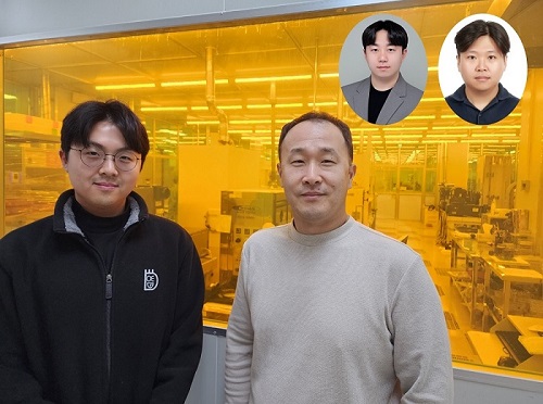 KAIST Innovates Mid-Infrared Photodetectors for Exoplanet Detection, Expanding Applications to Environmental and Medical Fields
NASA’s James Webb Space Telescope (JWST) utilizes mid-infrared spectroscopy to precisely analyze molecular components such as water vapor and sulfur dioxide in exoplanet atmospheres. The key to this analysis, where each molecule exhibits a unique spectral "fingerprint," lies in highly sensitive photodetector technology capable of measuring extremely weak light intensities. Recently, KAIST researchers have developed an innovative photodetector capable of detecting a broad range of mid-infrared spectra, garnering significant attention.
< Photo 1. (from the left) Ph.D. candidate Inki Kim (co-author), Professor SangHyeon Kim (corresponding author), Dr. Joonsup Shim (first author), and Dr. Jinha Lim (co-author) of KAIST School of Electrical Engineering. >
KAIST (represented by President Kwang-Hyung Lee) announced on the 27th of March that a research team led by Professor SangHyeon Kim from the School of Electrical Engineering has developed a mid-infrared photodetector that operates stably at room temperature, marking a major turning point for the commercialization of ultra-compact optical sensors.
The newly developed photodetector utilizes conventional silicon-based CMOS processes, enabling low-cost mass production while maintaining stable operation at room temperature. Notably, the research team successfully demonstrated the real-time detection of carbon dioxide (CO₂) gas using ultra-compact and ultra-thin optical sensors equipped with this photodetector, proving its potential for environmental monitoring and hazardous gas analysis.
Existing mid-infrared photodetectors generally require cooling systems due to high thermal noise at room temperature. These cooling systems increase the size and cost of equipment, making miniaturization and integration into portable devices challenging. Furthermore, conventional mid-infrared photodetectors are incompatible with silicon-based CMOS processes, limiting large-scale production and commercialization.
To address these limitations, the research team developed a waveguide-integrated photodetector using germanium (Ge), a Group IV element like silicon. This approach enables broad-spectrum mid-infrared detection while ensuring stable operation at room temperature.
< Figure 1. Schematic diagram of a room-temperature mid-infrared waveguide-integrated photodetector based on the Ge-on-insulator optical platform proposed in this study (top). Optical microscope image of the integrated photodetector connected with the sensing unit (bottom). >
A waveguide is a structure designed to efficiently guide light along a specific path with minimal loss. To implement various optical functions on a chip (on-chip), the development of waveguide-integrated photodetectors and waveguide-based optical components is essential.
Unlike conventional photodetectors that primarily rely on bandgap absorption principles, this new technology leverages the bolometric effect*, allowing it to detect the entire mid-infrared spectral range. As a result, it can be widely applied to the real-time sensing of various molecular species.
*Bolometric effect: A principle in which light absorption leads to an increase in temperature, causing electrical signals to change accordingly.
The waveguide-integrated mid-infrared photodetector developed by the research team is considered a groundbreaking innovation that overcomes the limitations of existing mid-infrared sensor technologies, including the need for cooling, difficulties in mass production, and high costs.
< Figure 2. Room temperature photoresponse characteristics of the mid-infrared waveguide photodetector proposed in this study (left) and real-time carbon dioxide (CO2) gas sensing results using the photodetector (right). >
This breakthrough technology is expected to be applicable across diverse fields, including environmental monitoring, medical diagnostics, industrial process management, national defense and security, and smart devices. It also paves the way for next-generation mid-infrared sensor advancements.
Professor SangHyeon Kim from KAIST stated, "This research represents a novel approach that overcomes the limitations of existing mid-infrared photodetector technologies and has great potential for practical applications in various fields." He further emphasized, "Since this sensor technology is compatible with CMOS processes, it enables low-cost mass production, making it highly suitable for next-generation environmental monitoring systems and smart manufacturing sites."
< Figure 3. Performance comparison image of a room-temperature mid-infrared waveguide photodetector fabricated with the technology proposed in this study. It achieves the world’s highest performance compared to existing technologies utilizing the Bolometric effect, and is the only solution compatible with CMOS processes. The technology proposed by our research team is characterized by its ability to respond to a wide spectrum of the mid-infrared band without limitations. >
The study, with Dr. Joonsup Shim (currently a postdoctoral researcher at Harvard University) as the first author, was published on March 19, 2025 in the internationally renowned journal Light: Science & Applications (JCR 2.9%, IF=20.6).
(Paper title: “Room-temperature waveguide-integrated photodetector using bolometric effect for mid-infrared spectroscopy applications,” https://doi.org/10.1038/s41377-025-01803-3)
2025.03.27 View 2454
KAIST Innovates Mid-Infrared Photodetectors for Exoplanet Detection, Expanding Applications to Environmental and Medical Fields
NASA’s James Webb Space Telescope (JWST) utilizes mid-infrared spectroscopy to precisely analyze molecular components such as water vapor and sulfur dioxide in exoplanet atmospheres. The key to this analysis, where each molecule exhibits a unique spectral "fingerprint," lies in highly sensitive photodetector technology capable of measuring extremely weak light intensities. Recently, KAIST researchers have developed an innovative photodetector capable of detecting a broad range of mid-infrared spectra, garnering significant attention.
< Photo 1. (from the left) Ph.D. candidate Inki Kim (co-author), Professor SangHyeon Kim (corresponding author), Dr. Joonsup Shim (first author), and Dr. Jinha Lim (co-author) of KAIST School of Electrical Engineering. >
KAIST (represented by President Kwang-Hyung Lee) announced on the 27th of March that a research team led by Professor SangHyeon Kim from the School of Electrical Engineering has developed a mid-infrared photodetector that operates stably at room temperature, marking a major turning point for the commercialization of ultra-compact optical sensors.
The newly developed photodetector utilizes conventional silicon-based CMOS processes, enabling low-cost mass production while maintaining stable operation at room temperature. Notably, the research team successfully demonstrated the real-time detection of carbon dioxide (CO₂) gas using ultra-compact and ultra-thin optical sensors equipped with this photodetector, proving its potential for environmental monitoring and hazardous gas analysis.
Existing mid-infrared photodetectors generally require cooling systems due to high thermal noise at room temperature. These cooling systems increase the size and cost of equipment, making miniaturization and integration into portable devices challenging. Furthermore, conventional mid-infrared photodetectors are incompatible with silicon-based CMOS processes, limiting large-scale production and commercialization.
To address these limitations, the research team developed a waveguide-integrated photodetector using germanium (Ge), a Group IV element like silicon. This approach enables broad-spectrum mid-infrared detection while ensuring stable operation at room temperature.
< Figure 1. Schematic diagram of a room-temperature mid-infrared waveguide-integrated photodetector based on the Ge-on-insulator optical platform proposed in this study (top). Optical microscope image of the integrated photodetector connected with the sensing unit (bottom). >
A waveguide is a structure designed to efficiently guide light along a specific path with minimal loss. To implement various optical functions on a chip (on-chip), the development of waveguide-integrated photodetectors and waveguide-based optical components is essential.
Unlike conventional photodetectors that primarily rely on bandgap absorption principles, this new technology leverages the bolometric effect*, allowing it to detect the entire mid-infrared spectral range. As a result, it can be widely applied to the real-time sensing of various molecular species.
*Bolometric effect: A principle in which light absorption leads to an increase in temperature, causing electrical signals to change accordingly.
The waveguide-integrated mid-infrared photodetector developed by the research team is considered a groundbreaking innovation that overcomes the limitations of existing mid-infrared sensor technologies, including the need for cooling, difficulties in mass production, and high costs.
< Figure 2. Room temperature photoresponse characteristics of the mid-infrared waveguide photodetector proposed in this study (left) and real-time carbon dioxide (CO2) gas sensing results using the photodetector (right). >
This breakthrough technology is expected to be applicable across diverse fields, including environmental monitoring, medical diagnostics, industrial process management, national defense and security, and smart devices. It also paves the way for next-generation mid-infrared sensor advancements.
Professor SangHyeon Kim from KAIST stated, "This research represents a novel approach that overcomes the limitations of existing mid-infrared photodetector technologies and has great potential for practical applications in various fields." He further emphasized, "Since this sensor technology is compatible with CMOS processes, it enables low-cost mass production, making it highly suitable for next-generation environmental monitoring systems and smart manufacturing sites."
< Figure 3. Performance comparison image of a room-temperature mid-infrared waveguide photodetector fabricated with the technology proposed in this study. It achieves the world’s highest performance compared to existing technologies utilizing the Bolometric effect, and is the only solution compatible with CMOS processes. The technology proposed by our research team is characterized by its ability to respond to a wide spectrum of the mid-infrared band without limitations. >
The study, with Dr. Joonsup Shim (currently a postdoctoral researcher at Harvard University) as the first author, was published on March 19, 2025 in the internationally renowned journal Light: Science & Applications (JCR 2.9%, IF=20.6).
(Paper title: “Room-temperature waveguide-integrated photodetector using bolometric effect for mid-infrared spectroscopy applications,” https://doi.org/10.1038/s41377-025-01803-3)
2025.03.27 View 2454 -
 KAIST Captures Hot Holes: A Breakthrough in Light-to-Electricity Energy Conversion
When light interacts with metallic nanostructures, it instantaneously generates plasmonic hot carriers, which serve as key intermediates for converting optical energy into high-value energy sources such as electricity and chemical energy. Among these, hot holes play a crucial role in enhancing photoelectrochemical reactions. However, they thermally dissipate within picoseconds (trillionths of a second), making practical applications challenging. Now, a Korean research team has successfully developed a method for sustaining hot holes longer and amplifying their flow, accelerating the commercialization of next-generation, high-efficiency, light-to-energy conversion technologies.
KAIST (represented by President Kwang Hyung Lee) announced on the 12th of March that a research team led by Distinguished Professor Jeong Young Park from the Department of Chemistry, in collaboration with Professor Moonsang Lee from the Department of Materials Science and Engineering at Inha University, has successfully amplified the flow of hot holes and mapped local current distribution in real time, thereby elucidating the mechanism of photocurrent enhancement.
The team designed a nanodiode structure by placing a metallic nanomesh on a specialized semiconductor substrate (p-type gallium nitride) to facilitate hot hole extraction at the surface. As a result, in gallium nitride substrates aligned with the hot hole extraction direction, the flow of hot holes was amplified by approximately two times compared to substrates aligned in other directions.
To fabricate the Au nanomesh, a polystyrene nano-bead monolayer assembly was first placed on a gallium nitride (p-GaN) substrate, and then the polystyrene nano-beads were etched to form a nanomesh template (Figure 1A). Then, a 20 nm thick gold nano-film was deposited, and the etched polystyrene nano-beads were removed to realize the gold nano-mesh structure on the GaN substrate (Figure 1B). The fabricated Au nanomesh exhibited strong light absorption in the visible range due to the plasmonic resonance effect (Figure 1C). >
Furthermore, using a photoconductive atomic force microscopy (pc-AFM)-based photocurrent mapping system, the researchers analyzed the flow of hot holes in real time at the nanometer scale (one hundred-thousandth the thickness of a human hair). They observed that hot hole activation was strongest at "hot spots," where light was locally concentrated on the gold nanomesh. However, by modifying the growth direction of the gallium nitride substrate, hot hole activation extended beyond the hot spots to other areas as well.
Through this research, the team discovered an efficient method for converting light into electrical and chemical energy. This breakthrough is expected to significantly advance next-generation solar cells, photocatalysts, and hydrogen production technologies.
Professor Jeong Young Park stated, "For the first time, we have successfully controlled the flow of hot holes using a nanodiode technique. This innovation holds great potential for various optoelectronic devices and photocatalytic applications. For example, it could lead to groundbreaking advancements in solar energy conversion technologies, such as solar cells and hydrogen production. Additionally, the real-time analysis technology we developed can be applied to the development of ultra-miniaturized optoelectronic devices, including optical sensors and nanoscale semiconductor components."
The study was led by Hyunhwa Lee (PhD., KAIST Department of Chemistry) and Yujin Park (Postdoc Researcher, University of Texas at Austin Department of Chemical Engineering) as co-first authors and Professors Moonsang Lee (Inha University, Department of Materials Science and Engineering) and Jeong Young Park (KAIST, Department of Chemistry) serving as corresponding authors. The research findings were published online in Science Advances on March 7.
(Paper Title: “Reconfiguring hot-hole flux via polarity modulation of p-GaN in plasmonic Schottky architectures”, DOI: https://www.science.org/doi/10.1126/sciadv.adu0086)
This research was supported by the National Research Foundation of Korea (NRF).
2025.03.17 View 3587
KAIST Captures Hot Holes: A Breakthrough in Light-to-Electricity Energy Conversion
When light interacts with metallic nanostructures, it instantaneously generates plasmonic hot carriers, which serve as key intermediates for converting optical energy into high-value energy sources such as electricity and chemical energy. Among these, hot holes play a crucial role in enhancing photoelectrochemical reactions. However, they thermally dissipate within picoseconds (trillionths of a second), making practical applications challenging. Now, a Korean research team has successfully developed a method for sustaining hot holes longer and amplifying their flow, accelerating the commercialization of next-generation, high-efficiency, light-to-energy conversion technologies.
KAIST (represented by President Kwang Hyung Lee) announced on the 12th of March that a research team led by Distinguished Professor Jeong Young Park from the Department of Chemistry, in collaboration with Professor Moonsang Lee from the Department of Materials Science and Engineering at Inha University, has successfully amplified the flow of hot holes and mapped local current distribution in real time, thereby elucidating the mechanism of photocurrent enhancement.
The team designed a nanodiode structure by placing a metallic nanomesh on a specialized semiconductor substrate (p-type gallium nitride) to facilitate hot hole extraction at the surface. As a result, in gallium nitride substrates aligned with the hot hole extraction direction, the flow of hot holes was amplified by approximately two times compared to substrates aligned in other directions.
To fabricate the Au nanomesh, a polystyrene nano-bead monolayer assembly was first placed on a gallium nitride (p-GaN) substrate, and then the polystyrene nano-beads were etched to form a nanomesh template (Figure 1A). Then, a 20 nm thick gold nano-film was deposited, and the etched polystyrene nano-beads were removed to realize the gold nano-mesh structure on the GaN substrate (Figure 1B). The fabricated Au nanomesh exhibited strong light absorption in the visible range due to the plasmonic resonance effect (Figure 1C). >
Furthermore, using a photoconductive atomic force microscopy (pc-AFM)-based photocurrent mapping system, the researchers analyzed the flow of hot holes in real time at the nanometer scale (one hundred-thousandth the thickness of a human hair). They observed that hot hole activation was strongest at "hot spots," where light was locally concentrated on the gold nanomesh. However, by modifying the growth direction of the gallium nitride substrate, hot hole activation extended beyond the hot spots to other areas as well.
Through this research, the team discovered an efficient method for converting light into electrical and chemical energy. This breakthrough is expected to significantly advance next-generation solar cells, photocatalysts, and hydrogen production technologies.
Professor Jeong Young Park stated, "For the first time, we have successfully controlled the flow of hot holes using a nanodiode technique. This innovation holds great potential for various optoelectronic devices and photocatalytic applications. For example, it could lead to groundbreaking advancements in solar energy conversion technologies, such as solar cells and hydrogen production. Additionally, the real-time analysis technology we developed can be applied to the development of ultra-miniaturized optoelectronic devices, including optical sensors and nanoscale semiconductor components."
The study was led by Hyunhwa Lee (PhD., KAIST Department of Chemistry) and Yujin Park (Postdoc Researcher, University of Texas at Austin Department of Chemical Engineering) as co-first authors and Professors Moonsang Lee (Inha University, Department of Materials Science and Engineering) and Jeong Young Park (KAIST, Department of Chemistry) serving as corresponding authors. The research findings were published online in Science Advances on March 7.
(Paper Title: “Reconfiguring hot-hole flux via polarity modulation of p-GaN in plasmonic Schottky architectures”, DOI: https://www.science.org/doi/10.1126/sciadv.adu0086)
This research was supported by the National Research Foundation of Korea (NRF).
2025.03.17 View 3587 -
 KAIST develops a new, bone-like material that strengthens with use in collaboration with GIT
Materials used in apartment buildings, vehicles, and other structures deteriorate over time under repeated loads, leading to failure and breakage. A joint research team from Korea and the United States has successfully developed a bioinspired material that becomes stronger with use, taking inspiration from the way bones synthesize minerals from bodily fluids under stress, increasing bone density.
< (From left) Professor Sung Hoon Kang of the Department of Materials Science and Engineering, Johns Hopkins University Ph.D. candidates Bohan Sun and Grant Kitchen, Professor Yuhang Hu and Ph.D. candidate Dongjung He of Georgia Institute of Technology >
KAIST (represented by President Kwang Hyung Lee) announced on the 20th of February that a research team led by Professor Sung Hoon Kang from the Department of Materials Science and Engineering, in collaboration with Johns Hopkins University and the Georgia Institute of Technology, had developed a new material that strengthens with repeated use, similar to how bones become stronger with exercise.
Professor Kang’s team sought to address the issue of conventional materials degrading with repeated use. Inspired by the biological process where stress triggers cells to form minerals that strengthen bones, the team developed a material that synthesizes minerals under stress without relying on cellular activity. This innovation is expected to enable applications in a variety of fields.
To replace the function of cells, the research team created a porous piezoelectric substrate that converts mechanical force into electricity and actually generates more charge under greater force. They then synthesized a composite material by infusing it with an electrolyte containing mineral components similar to those in blood.
< Figure 1. Schematic diagram of the biomimetic concept based on bone and pitcher plants, the reversible strengthening mechanism, the process of fabricating porous composites, the mechanical property changes with increasing stiffness and energy dissipation after cyclic loading, and the reprogrammable self-folding mechanism and applications >
After subjecting the material to periodic forces and measuring changes in its properties, they observed that its stiffness increased proportionally with the frequency and magnitude of stress and that its energy dissipation capability improved.
The reason for such properties was found to be due to minerals forming inside the porous material under repeated stress, as observed through micro-CT imaging of its internal structure. When subjected to large forces, these minerals fractured and dissipated energy, only to reform under further cyclic stress.
Unlike conventional materials that weaken with repeated use, this new material simultaneously enhances stiffness and impact absorption over time.
< Figure 2. Comparison of the changes in properties of the newly developed new material (LIPPS) with other materials under cyclic loading. (A) Graph showing the relative change rate of energy dissipation after cyclic loading and the relative change rate of elastic modulus upon unloading. LIPPS is in a new area that existing materials have not reached, and shows the characteristics of simultaneous increases in elastic modulus and energy dissipation. (B) Graph comparing the performance of LIPPS with current state-of-the-art mechanically adaptive materials. (Left) The maximum property change rate compared to the baseline after cyclic loading, LIPPS shows much higher changes in elastic modulus, dissipated energy density and ratio, toughness (impact resistance), and stored energy density than the existing adaptive materials. (Right) The absolute value range of the reported properties before and after cyclic loading shows that LIPPS has higher elastic modulus and toughness than the existing adaptive materials. >
Moreover, because its properties improve in proportion to the magnitude and frequency of applied stress, it can self-adjust to achieve mechanical property distributions suitable for different structural applications. It also possesses self-healing capabilities.
Professor Kang stated, "This newly developed material, which strengthens and absorbs impact better with repeated use compared to conventional materials, holds great potential for applications in artificial joints, as well as in aircraft, ships, automobiles, and structural engineering."
This study, with Professor Sung Hoon Kang as the corresponding author, was published in Science Advances (Vol. 11, Issue 6, February).
(Paper title: “A material dynamically enhancing both load-bearing and energy-dissipation capability under cyclic loading”) DOI: 10.1126/sciadv.adt3979
This research was conducted as a joint effort with Johns Hopkins University's Extreme Materials Institute and the Georgia Institute of Technology, supported by the National Research Foundation of Korea’s Brain Pool Plus program.
2025.02.22 View 3079
KAIST develops a new, bone-like material that strengthens with use in collaboration with GIT
Materials used in apartment buildings, vehicles, and other structures deteriorate over time under repeated loads, leading to failure and breakage. A joint research team from Korea and the United States has successfully developed a bioinspired material that becomes stronger with use, taking inspiration from the way bones synthesize minerals from bodily fluids under stress, increasing bone density.
< (From left) Professor Sung Hoon Kang of the Department of Materials Science and Engineering, Johns Hopkins University Ph.D. candidates Bohan Sun and Grant Kitchen, Professor Yuhang Hu and Ph.D. candidate Dongjung He of Georgia Institute of Technology >
KAIST (represented by President Kwang Hyung Lee) announced on the 20th of February that a research team led by Professor Sung Hoon Kang from the Department of Materials Science and Engineering, in collaboration with Johns Hopkins University and the Georgia Institute of Technology, had developed a new material that strengthens with repeated use, similar to how bones become stronger with exercise.
Professor Kang’s team sought to address the issue of conventional materials degrading with repeated use. Inspired by the biological process where stress triggers cells to form minerals that strengthen bones, the team developed a material that synthesizes minerals under stress without relying on cellular activity. This innovation is expected to enable applications in a variety of fields.
To replace the function of cells, the research team created a porous piezoelectric substrate that converts mechanical force into electricity and actually generates more charge under greater force. They then synthesized a composite material by infusing it with an electrolyte containing mineral components similar to those in blood.
< Figure 1. Schematic diagram of the biomimetic concept based on bone and pitcher plants, the reversible strengthening mechanism, the process of fabricating porous composites, the mechanical property changes with increasing stiffness and energy dissipation after cyclic loading, and the reprogrammable self-folding mechanism and applications >
After subjecting the material to periodic forces and measuring changes in its properties, they observed that its stiffness increased proportionally with the frequency and magnitude of stress and that its energy dissipation capability improved.
The reason for such properties was found to be due to minerals forming inside the porous material under repeated stress, as observed through micro-CT imaging of its internal structure. When subjected to large forces, these minerals fractured and dissipated energy, only to reform under further cyclic stress.
Unlike conventional materials that weaken with repeated use, this new material simultaneously enhances stiffness and impact absorption over time.
< Figure 2. Comparison of the changes in properties of the newly developed new material (LIPPS) with other materials under cyclic loading. (A) Graph showing the relative change rate of energy dissipation after cyclic loading and the relative change rate of elastic modulus upon unloading. LIPPS is in a new area that existing materials have not reached, and shows the characteristics of simultaneous increases in elastic modulus and energy dissipation. (B) Graph comparing the performance of LIPPS with current state-of-the-art mechanically adaptive materials. (Left) The maximum property change rate compared to the baseline after cyclic loading, LIPPS shows much higher changes in elastic modulus, dissipated energy density and ratio, toughness (impact resistance), and stored energy density than the existing adaptive materials. (Right) The absolute value range of the reported properties before and after cyclic loading shows that LIPPS has higher elastic modulus and toughness than the existing adaptive materials. >
Moreover, because its properties improve in proportion to the magnitude and frequency of applied stress, it can self-adjust to achieve mechanical property distributions suitable for different structural applications. It also possesses self-healing capabilities.
Professor Kang stated, "This newly developed material, which strengthens and absorbs impact better with repeated use compared to conventional materials, holds great potential for applications in artificial joints, as well as in aircraft, ships, automobiles, and structural engineering."
This study, with Professor Sung Hoon Kang as the corresponding author, was published in Science Advances (Vol. 11, Issue 6, February).
(Paper title: “A material dynamically enhancing both load-bearing and energy-dissipation capability under cyclic loading”) DOI: 10.1126/sciadv.adt3979
This research was conducted as a joint effort with Johns Hopkins University's Extreme Materials Institute and the Georgia Institute of Technology, supported by the National Research Foundation of Korea’s Brain Pool Plus program.
2025.02.22 View 3079