OT
-
 Experts to Help Asia Navigate the Post-COVID-19 and 4IR Eras
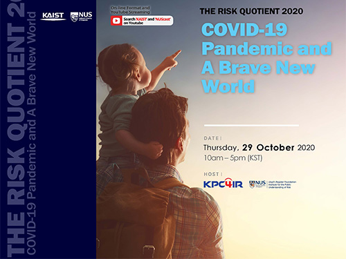
Risk Quotient 2020, an international conference co-hosted by KAIST and the National University of Singapore (NUS), will bring together world-leading experts from academia and industry to help Asia navigate the post-COVID-19 and Fourth Industrial Revolution (4IR) eras.
The online conference will be held on October 29 from 10 a.m. Korean time under the theme “COVID-19 Pandemic and A Brave New World”. It will be streamed live on YouTube at https://www.youtube.com/c/KAISTofficial and https://www.youtube.com/user/NUScast.
The Korea Policy Center for the Fourth Industrial Revolution (KPC4IR) at KAIST organized this conference in collaboration with the Lloyd's Register Foundation Institute for the Public Understanding of Risk (IPUR) at NUS.
During the conference, global leaders will examine the socioeconomic impacts of the COVID-19 pandemic on areas including digital innovation, education, the workforce, and the economy. They will then highlight digital and 4IR technologies that could be utilized to effectively mitigate the risks and challenges associated with the pandemic, while harnessing the opportunities that these socioeconomic effects may present. Their discussions will mainly focus on the Asian region.
In his opening remarks, KAIST President Sung-Chul Shin will express his appreciation for the Asian populations’ greater trust in and compliance with their governments, which have given the continent a leg up against the coronavirus. He will then emphasize that by working together through the exchange of ideas and global collaboration, we will be able to shape ‘a brave new world’ to better humanity. Welcoming remarks by Prof. Sang Yup Lee (Dean, KAIST Institutes) and Prof. Tze Yun Leong (Director, AI Technology at AI Singapore) will follow.
For the keynote speech, Prof. Lan Xue (Dean, Schwarzman College, Tsinghua University) will share China’s response to COVID-19 and lessons for crisis management. Prof. Danny Quah (Dean, Lee Kuan Yew School of Public Policy, NUS) will present possible ways to overcome these difficult times. Dr. Kak-Soo Shin (Senior Advisor, Shin & Kim LLC, Former Ambassador to the State of Israel and Japan, and Former First and Second Vice Minister of the Ministry of Foreign Affairs of the Republic of Korea) will stress the importance of the international community’s solidarity to ensure peace, prosperity, and safety in this new era.
Panel Session I will address the impact of COVID-19 on digital innovation. Dr. Carol Soon (Senior Research Fellow, Institute of Policy Studies, NUS) will present her interpretation of recent technological developments as both opportunities for our society as a whole and challenges for vulnerable groups such as low-income families. Dr. Christopher SungWook Chang (Managing Director, Kakao Mobility) will show how changes in mobility usage patterns can be captured by Kakao Mobility’s big data analysis. He will illustrate how the data can be used to interpret citizen’s behaviors and how risks can be transformed into opportunities by utilizing technology. Mr. Steve Ledzian’s (Vice President, Chief Technology Officer, FireEye) talk will discuss the dangers caused by threat actors and other cyber risk implications of COVID-19. Dr. June Sung Park (Chairman, Korea Software Technology Association (KOSTA)) will share how COVID-19 has accelerated digital transformations across all industries and why software education should be reformed to improve Korea’s competitiveness.
Panel Session II will examine the impact on education and the workforce. Dr. Sang-Jin Ban (President, Korean Educational Development Institute (KEDI)) will explain Korea’s educational response to the pandemic and the concept of “blended learning” as a new paradigm, and present both positive and negative impacts of online education on students’ learning experiences. Prof. Reuben Ng (Professor, Lee Kuan Yew School of Public Policy, NUS) will present on graduate underemployment, which seems to have worsened during COVID-19. Dr. Michael Fung’s presentation (Deputy Chief Executive (Industry), SkillsFuture SG) will introduce the promotion of lifelong learning in Singapore through a new national initiative known as the ‘SkillsFuture Movement’. This movement serves as an example of a national response to disruptions in the job market and the pace of skills obsolescence triggered by AI and COVID-19.
Panel Session III will touch on technology leadership and Asia’s digital economy and society. Prof. Naubahar Sharif (Professor, Division of Social Science and Division of Public Policy, Hong Kong University of Science and Technology (HKUST)) will share his views on the potential of China in taking over global technological leadership based on its massive domestic market, its government support, and the globalization process. Prof. Yee Kuang Heng (Professor, Graduate School of Public Policy, University of Tokyo) will illustrate how different legal and political needs in China and Japan have shaped the ways technologies have been deployed in responding to COVID-19. Dr. Hayun Kang (Head, International Cooperation Research Division, Korea Information Society Development Institute (KISDI)) will explain Korea’s relative success containing the pandemic compared to other countries, and how policy leaders and institutions that embrace digital technologies in the pursuit of public welfare objectives can produce positive outcomes while minimizing the side effects.
Prof. Kyung Ryul Park (Graduate School of Science and Technology Policy, KAIST) will be hosting the entire conference, whereas Prof. Alice Hae Yun Oh (Director, MARS Artificial Intelligence Research Center, KAIST), Prof. Wonjoon Kim (Dean, Graduate School of Innovation and Technology Management, College of Business, KAIST), Prof. Youngsun Kwon (Dean, KAIST Academy), and Prof. Taejun Lee (Korea Development Institute (KDI) School of Public Policy and Management) are to chair discussions with the keynote speakers and panelists.
Closing remarks will be delivered by Prof. Chan Ghee Koh (Director, NUS IPUR), Prof. So Young Kim (Director, KAIST KPC4IR), and Prof. Joungho Kim (Director, KAIST Global Strategy Institute (GSI)).
“This conference is expected to serve as a springboard to help Asian countries recover from global crises such as the COVID-19 pandemic through active cooperation and joint engagement among scholars, experts, and policymakers,” according to Director So Young Kim.
(END)
2020.10.22 View 17692
Experts to Help Asia Navigate the Post-COVID-19 and 4IR Eras
Risk Quotient 2020, an international conference co-hosted by KAIST and the National University of Singapore (NUS), will bring together world-leading experts from academia and industry to help Asia navigate the post-COVID-19 and Fourth Industrial Revolution (4IR) eras.
The online conference will be held on October 29 from 10 a.m. Korean time under the theme “COVID-19 Pandemic and A Brave New World”. It will be streamed live on YouTube at https://www.youtube.com/c/KAISTofficial and https://www.youtube.com/user/NUScast.
The Korea Policy Center for the Fourth Industrial Revolution (KPC4IR) at KAIST organized this conference in collaboration with the Lloyd's Register Foundation Institute for the Public Understanding of Risk (IPUR) at NUS.
During the conference, global leaders will examine the socioeconomic impacts of the COVID-19 pandemic on areas including digital innovation, education, the workforce, and the economy. They will then highlight digital and 4IR technologies that could be utilized to effectively mitigate the risks and challenges associated with the pandemic, while harnessing the opportunities that these socioeconomic effects may present. Their discussions will mainly focus on the Asian region.
In his opening remarks, KAIST President Sung-Chul Shin will express his appreciation for the Asian populations’ greater trust in and compliance with their governments, which have given the continent a leg up against the coronavirus. He will then emphasize that by working together through the exchange of ideas and global collaboration, we will be able to shape ‘a brave new world’ to better humanity. Welcoming remarks by Prof. Sang Yup Lee (Dean, KAIST Institutes) and Prof. Tze Yun Leong (Director, AI Technology at AI Singapore) will follow.
For the keynote speech, Prof. Lan Xue (Dean, Schwarzman College, Tsinghua University) will share China’s response to COVID-19 and lessons for crisis management. Prof. Danny Quah (Dean, Lee Kuan Yew School of Public Policy, NUS) will present possible ways to overcome these difficult times. Dr. Kak-Soo Shin (Senior Advisor, Shin & Kim LLC, Former Ambassador to the State of Israel and Japan, and Former First and Second Vice Minister of the Ministry of Foreign Affairs of the Republic of Korea) will stress the importance of the international community’s solidarity to ensure peace, prosperity, and safety in this new era.
Panel Session I will address the impact of COVID-19 on digital innovation. Dr. Carol Soon (Senior Research Fellow, Institute of Policy Studies, NUS) will present her interpretation of recent technological developments as both opportunities for our society as a whole and challenges for vulnerable groups such as low-income families. Dr. Christopher SungWook Chang (Managing Director, Kakao Mobility) will show how changes in mobility usage patterns can be captured by Kakao Mobility’s big data analysis. He will illustrate how the data can be used to interpret citizen’s behaviors and how risks can be transformed into opportunities by utilizing technology. Mr. Steve Ledzian’s (Vice President, Chief Technology Officer, FireEye) talk will discuss the dangers caused by threat actors and other cyber risk implications of COVID-19. Dr. June Sung Park (Chairman, Korea Software Technology Association (KOSTA)) will share how COVID-19 has accelerated digital transformations across all industries and why software education should be reformed to improve Korea’s competitiveness.
Panel Session II will examine the impact on education and the workforce. Dr. Sang-Jin Ban (President, Korean Educational Development Institute (KEDI)) will explain Korea’s educational response to the pandemic and the concept of “blended learning” as a new paradigm, and present both positive and negative impacts of online education on students’ learning experiences. Prof. Reuben Ng (Professor, Lee Kuan Yew School of Public Policy, NUS) will present on graduate underemployment, which seems to have worsened during COVID-19. Dr. Michael Fung’s presentation (Deputy Chief Executive (Industry), SkillsFuture SG) will introduce the promotion of lifelong learning in Singapore through a new national initiative known as the ‘SkillsFuture Movement’. This movement serves as an example of a national response to disruptions in the job market and the pace of skills obsolescence triggered by AI and COVID-19.
Panel Session III will touch on technology leadership and Asia’s digital economy and society. Prof. Naubahar Sharif (Professor, Division of Social Science and Division of Public Policy, Hong Kong University of Science and Technology (HKUST)) will share his views on the potential of China in taking over global technological leadership based on its massive domestic market, its government support, and the globalization process. Prof. Yee Kuang Heng (Professor, Graduate School of Public Policy, University of Tokyo) will illustrate how different legal and political needs in China and Japan have shaped the ways technologies have been deployed in responding to COVID-19. Dr. Hayun Kang (Head, International Cooperation Research Division, Korea Information Society Development Institute (KISDI)) will explain Korea’s relative success containing the pandemic compared to other countries, and how policy leaders and institutions that embrace digital technologies in the pursuit of public welfare objectives can produce positive outcomes while minimizing the side effects.
Prof. Kyung Ryul Park (Graduate School of Science and Technology Policy, KAIST) will be hosting the entire conference, whereas Prof. Alice Hae Yun Oh (Director, MARS Artificial Intelligence Research Center, KAIST), Prof. Wonjoon Kim (Dean, Graduate School of Innovation and Technology Management, College of Business, KAIST), Prof. Youngsun Kwon (Dean, KAIST Academy), and Prof. Taejun Lee (Korea Development Institute (KDI) School of Public Policy and Management) are to chair discussions with the keynote speakers and panelists.
Closing remarks will be delivered by Prof. Chan Ghee Koh (Director, NUS IPUR), Prof. So Young Kim (Director, KAIST KPC4IR), and Prof. Joungho Kim (Director, KAIST Global Strategy Institute (GSI)).
“This conference is expected to serve as a springboard to help Asian countries recover from global crises such as the COVID-19 pandemic through active cooperation and joint engagement among scholars, experts, and policymakers,” according to Director So Young Kim.
(END)
2020.10.22 View 17692 -
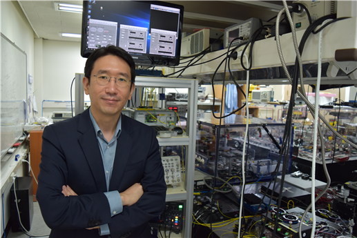 Scientist of October: Professor Jungwon Kim
Professor Jungwon Kim from the Department of Mechanical Engineering was selected as the ‘Scientist of the Month’ for October 2020 by the Ministry of Science and ICT and the National Research Foundation of Korea. Professor Kim was recognized for his contributions to expanding the horizons of the basics of precision engineering through his research on multifunctional ultrahigh-speed, high-resolution sensors. He received 10 million KRW in prize money.
Professor Kim was selected as the recipient of this award in celebration of “Measurement Day”, which commemorates October 26 as the day in which King Sejong the Great established a volume measurement system.
Professor Kim discovered that the time difference between the pulse of light created by a laser and the pulse of the current produced by a light-emitting diode was as small as 100 attoseconds (10-16 seconds). He then developed a unique multifunctional ultrahigh-speed, high-resolution Time-of-Flight (TOF) sensor that could take measurements of multiple points at the same time by sampling electric light. The sensor, with a measurement speed of 100 megahertz (100 million vibrations per second), a resolution of 180 picometers (1/5.5 billion meters), and a dynamic range of 150 decibels, overcame the limitations of both existing TOF techniques and laser interferometric techniques at the same time. The results of this research were published in Nature Photonics on February 10, 2020.
Professor Kim said, “I’d like to thank the graduate students who worked passionately with me, and KAIST for providing an environment in which I could fully focus on research. I am looking forward to the new and diverse applications in the field of machine manufacturing, such as studying the dynamic phenomena in microdevices, or taking ultraprecision measurement of shapes for advanced manufacturing.”
(END)
2020.10.15 View 14881
Scientist of October: Professor Jungwon Kim
Professor Jungwon Kim from the Department of Mechanical Engineering was selected as the ‘Scientist of the Month’ for October 2020 by the Ministry of Science and ICT and the National Research Foundation of Korea. Professor Kim was recognized for his contributions to expanding the horizons of the basics of precision engineering through his research on multifunctional ultrahigh-speed, high-resolution sensors. He received 10 million KRW in prize money.
Professor Kim was selected as the recipient of this award in celebration of “Measurement Day”, which commemorates October 26 as the day in which King Sejong the Great established a volume measurement system.
Professor Kim discovered that the time difference between the pulse of light created by a laser and the pulse of the current produced by a light-emitting diode was as small as 100 attoseconds (10-16 seconds). He then developed a unique multifunctional ultrahigh-speed, high-resolution Time-of-Flight (TOF) sensor that could take measurements of multiple points at the same time by sampling electric light. The sensor, with a measurement speed of 100 megahertz (100 million vibrations per second), a resolution of 180 picometers (1/5.5 billion meters), and a dynamic range of 150 decibels, overcame the limitations of both existing TOF techniques and laser interferometric techniques at the same time. The results of this research were published in Nature Photonics on February 10, 2020.
Professor Kim said, “I’d like to thank the graduate students who worked passionately with me, and KAIST for providing an environment in which I could fully focus on research. I am looking forward to the new and diverse applications in the field of machine manufacturing, such as studying the dynamic phenomena in microdevices, or taking ultraprecision measurement of shapes for advanced manufacturing.”
(END)
2020.10.15 View 14881 -
 Sturdy Fabric-Based Piezoelectric Energy Harvester Takes Us One Step Closer to Wearable Electronics
KAIST researchers presented a highly flexible but sturdy wearable piezoelectric harvester using the simple and easy fabrication process of hot pressing and tape casting. This energy harvester, which has record high interfacial adhesion strength, will take us one step closer to being able to manufacture embedded wearable electronics.
A research team led by Professor Seungbum Hong said that the novelty of this result lies in its simplicity, applicability, durability, and its new characterization of wearable electronic devices.
Wearable devices are increasingly being used in a wide array of applications from small electronics to embedded devices such as sensors, actuators, displays, and energy harvesters.
Despite their many advantages, high costs and complex fabrication processes remained challenges for reaching commercialization. In addition, their durability was frequently questioned. To address these issues, Professor Hong’s team developed a new fabrication process and analysis technology for testing the mechanical properties of affordable wearable devices.
For this process, the research team used a hot pressing and tape casting procedure to connect the fabric structures of polyester and a polymer film. Hot pressing has usually been used when making batteries and fuel cells due to its high adhesiveness. Above all, the process takes only two to three minutes.
The newly developed fabrication process will enable the direct application of a device into general garments using hot pressing just as graphic patches can be attached to garments using a heat press.
In particular, when the polymer film is hot pressed onto a fabric below its crystallization temperature, it transforms into an amorphous state. In this state, it compactly attaches to the concave surface of the fabric and infiltrates into the gaps between the transverse wefts and longitudinal warps. These features result in high interfacial adhesion strength. For this reason, hot pressing has the potential to reduce the cost of fabrication through the direct application of fabric-based wearable devices to common garments.
In addition to the conventional durability test of bending cycles, the newly introduced surface and interfacial cutting analysis system proved the high mechanical durability of the fabric-based wearable device by measuring the high interfacial adhesion strength between the fabric and the polymer film. Professor Hong said the study lays a new foundation for the manufacturing process and analysis of wearable devices using fabrics and polymers.
He added that his team first used the surface and interfacial cutting analysis system (SAICAS) in the field of wearable electronics to test the mechanical properties of polymer-based wearable devices. Their surface and interfacial cutting analysis system is more precise than conventional methods (peel test, tape test, and microstretch test) because it qualitatively and quantitatively measures the adhesion strength.
Professor Hong explained, “This study could enable the commercialization of highly durable wearable devices based on the analysis of their interfacial adhesion strength. Our study lays a new foundation for the manufacturing process and analysis of other devices using fabrics and polymers. We look forward to fabric-based wearable electronics hitting the market very soon.”
The results of this study were registered as a domestic patent in Korea last year, and published in Nano Energy this month. This study has been conducted through collaboration with Professor Yong Min Lee in the Department of Energy Science and Engineering at DGIST, Professor Kwangsoo No in the Department of Materials Science and Engineering at KAIST, and Professor Seunghwa Ryu in the Department of Mechanical Engineering at KAIST.
This study was supported by the High-Risk High-Return Project and the Global Singularity Research Project at KAIST, the National Research Foundation, and the Ministry of Science and ICT in Korea.
-Publication:
Jaegyu Kim, Seoungwoo Byun, Sangryun Lee, Jeongjae Ryu, Seongwoo Cho, Chungik Oh, Hongjun Kim, Kwangsoo No, Seunghwa Ryu, Yong Min Lee, Seungbum Hong*, Nano Energy 75 (2020), 104992.
https://doi.org/10.1016/j.nanoen.2020.104992
-Profile: Professor Seungbum Hong
seungbum@kaist.ac.kr
http://mii.kaist.ac.kr/
Department of Materials Science and Engineering
KAIST
2020.09.17 View 15980
Sturdy Fabric-Based Piezoelectric Energy Harvester Takes Us One Step Closer to Wearable Electronics
KAIST researchers presented a highly flexible but sturdy wearable piezoelectric harvester using the simple and easy fabrication process of hot pressing and tape casting. This energy harvester, which has record high interfacial adhesion strength, will take us one step closer to being able to manufacture embedded wearable electronics.
A research team led by Professor Seungbum Hong said that the novelty of this result lies in its simplicity, applicability, durability, and its new characterization of wearable electronic devices.
Wearable devices are increasingly being used in a wide array of applications from small electronics to embedded devices such as sensors, actuators, displays, and energy harvesters.
Despite their many advantages, high costs and complex fabrication processes remained challenges for reaching commercialization. In addition, their durability was frequently questioned. To address these issues, Professor Hong’s team developed a new fabrication process and analysis technology for testing the mechanical properties of affordable wearable devices.
For this process, the research team used a hot pressing and tape casting procedure to connect the fabric structures of polyester and a polymer film. Hot pressing has usually been used when making batteries and fuel cells due to its high adhesiveness. Above all, the process takes only two to three minutes.
The newly developed fabrication process will enable the direct application of a device into general garments using hot pressing just as graphic patches can be attached to garments using a heat press.
In particular, when the polymer film is hot pressed onto a fabric below its crystallization temperature, it transforms into an amorphous state. In this state, it compactly attaches to the concave surface of the fabric and infiltrates into the gaps between the transverse wefts and longitudinal warps. These features result in high interfacial adhesion strength. For this reason, hot pressing has the potential to reduce the cost of fabrication through the direct application of fabric-based wearable devices to common garments.
In addition to the conventional durability test of bending cycles, the newly introduced surface and interfacial cutting analysis system proved the high mechanical durability of the fabric-based wearable device by measuring the high interfacial adhesion strength between the fabric and the polymer film. Professor Hong said the study lays a new foundation for the manufacturing process and analysis of wearable devices using fabrics and polymers.
He added that his team first used the surface and interfacial cutting analysis system (SAICAS) in the field of wearable electronics to test the mechanical properties of polymer-based wearable devices. Their surface and interfacial cutting analysis system is more precise than conventional methods (peel test, tape test, and microstretch test) because it qualitatively and quantitatively measures the adhesion strength.
Professor Hong explained, “This study could enable the commercialization of highly durable wearable devices based on the analysis of their interfacial adhesion strength. Our study lays a new foundation for the manufacturing process and analysis of other devices using fabrics and polymers. We look forward to fabric-based wearable electronics hitting the market very soon.”
The results of this study were registered as a domestic patent in Korea last year, and published in Nano Energy this month. This study has been conducted through collaboration with Professor Yong Min Lee in the Department of Energy Science and Engineering at DGIST, Professor Kwangsoo No in the Department of Materials Science and Engineering at KAIST, and Professor Seunghwa Ryu in the Department of Mechanical Engineering at KAIST.
This study was supported by the High-Risk High-Return Project and the Global Singularity Research Project at KAIST, the National Research Foundation, and the Ministry of Science and ICT in Korea.
-Publication:
Jaegyu Kim, Seoungwoo Byun, Sangryun Lee, Jeongjae Ryu, Seongwoo Cho, Chungik Oh, Hongjun Kim, Kwangsoo No, Seunghwa Ryu, Yong Min Lee, Seungbum Hong*, Nano Energy 75 (2020), 104992.
https://doi.org/10.1016/j.nanoen.2020.104992
-Profile: Professor Seungbum Hong
seungbum@kaist.ac.kr
http://mii.kaist.ac.kr/
Department of Materials Science and Engineering
KAIST
2020.09.17 View 15980 -
 Atomic Force Microscopy Reveals Nanoscale Dental Erosion from Beverages
KAIST researchers used atomic force microscopy to quantitatively evaluate how acidic and sugary drinks affect human tooth enamel at the nanoscale level. This novel approach is useful for measuring mechanical and morphological changes that occur over time during enamel erosion induced by beverages.
Enamel is the hard-white substance that forms the outer part of a tooth. It is the hardest substance in the human body, even stronger than bone. Its resilient surface is 96 percent mineral, the highest percentage of any body tissue, making it durable and damage-resistant. The enamel acts as a barrier to protect the soft inner layers of the tooth, but can become susceptible to degradation by acids and sugars.
Enamel erosion occurs when the tooth enamel is overexposed to excessive consumption of acidic and sugary food and drinks. The loss of enamel, if left untreated, can lead to various tooth conditions including stains, fractures, sensitivity, and translucence. Once tooth enamel is damaged, it cannot be brought back. Therefore, thorough studies on how enamel erosion starts and develops, especially at the initial stages, are of high scientific and clinical relevance for dental health maintenance.
A research team led by Professor Seungbum Hong from the Department of Materials Science and Engineering at KAIST reported a new method of applying atomic force microscopy (AFM) techniques to study the nanoscale characterization of this early stage of enamel erosion. This study was introduced in the Journal of the Mechanical Behavior of Biomedical Materials (JMBBM) on June 29.
AFM is a very-high-resolution type of scanning probe microscopy (SPM), with demonstrated resolution on the order of fractions of a nanometer (nm) that is equal to one billionth of a meter. AFM generates images by scanning a small cantilever over the surface of a sample, and this can precisely measure the structure and mechanical properties of the sample, such as surface roughness and elastic modulus.
The co-lead authors of the study, Dr. Panpan Li and Dr. Chungik Oh, chose three commercially available popular beverages, Coca-Cola®, Sprite®, and Minute Maid® orange juice, and immersed tooth enamel in these drinks over time to analyze their impacts on human teeth and monitor the etching process on tooth enamel.
Five healthy human molars were obtained from volunteers between age 20 and 35 who visited the KAIST Clinic. After extraction, the teeth were preserved in distilled water before the experiment. The drinks were purchased and opened right before the immersion experiment, and the team utilized AFM to measure the surface topography and elastic modulus map.
The researchers observed that the surface roughness of the tooth enamel increased significantly as the immersion time increased, while the elastic modulus of the enamel surface decreased drastically. It was demonstrated that the enamel surface roughened five times more when it was immersed in beverages for 10 minutes, and that the elastic modulus of tooth enamel was five times lower after five minutes in the drinks.
Additionally, the research team found preferential etching in scratched tooth enamel. Brushing your teeth too hard and toothpastes with polishing particles that are advertised to remove dental biofilms can cause scratches on the enamel surface, which can be preferential sites for etching, the study revealed.
Professor Hong said, “Our study shows that AFM is a suitable technique to characterize variations in the morphology and mechanical properties of dental erosion quantitatively at the nanoscale level.”
This work was supported by the National Research Foundation (NRF), the Ministry of Science and ICT (MSIT), and the KUSTAR-KAIST Institute of Korea.
A dentist at the KAIST Clinic, Dr. Suebean Cho, Dr. Sangmin Shin from the Smile Well Dental, and Professor Kack-Kyun Kim at the Seoul National University School of Dentistry also collaborated in this project.
Publication:
Li, P., et al. (2020) ‘Nanoscale effects of beverages on enamel surface of human teeth: An atomic force microscopy study’. Journal of the Mechanical Behavior of Biomedical Materials (JMBBM), Volume 110. Article No. 103930. Available online at https://doi.org/10.1016/j.jmbbm.2020.103930
Profile: Seungbum Hong, Ph.D.
Associate Professor
seungbum@kaist.ac.kr
http://mii.kaist.ac.kr/
Materials Imaging and Integration (MII) Lab.
Department of Materials Science and Engineering (MSE)
Korea Advanced Institute of Science and Technology (KAIST)
https://www.kaist.ac.kr
Daejeon 34141, Korea
(END)
2020.07.21 View 15082
Atomic Force Microscopy Reveals Nanoscale Dental Erosion from Beverages
KAIST researchers used atomic force microscopy to quantitatively evaluate how acidic and sugary drinks affect human tooth enamel at the nanoscale level. This novel approach is useful for measuring mechanical and morphological changes that occur over time during enamel erosion induced by beverages.
Enamel is the hard-white substance that forms the outer part of a tooth. It is the hardest substance in the human body, even stronger than bone. Its resilient surface is 96 percent mineral, the highest percentage of any body tissue, making it durable and damage-resistant. The enamel acts as a barrier to protect the soft inner layers of the tooth, but can become susceptible to degradation by acids and sugars.
Enamel erosion occurs when the tooth enamel is overexposed to excessive consumption of acidic and sugary food and drinks. The loss of enamel, if left untreated, can lead to various tooth conditions including stains, fractures, sensitivity, and translucence. Once tooth enamel is damaged, it cannot be brought back. Therefore, thorough studies on how enamel erosion starts and develops, especially at the initial stages, are of high scientific and clinical relevance for dental health maintenance.
A research team led by Professor Seungbum Hong from the Department of Materials Science and Engineering at KAIST reported a new method of applying atomic force microscopy (AFM) techniques to study the nanoscale characterization of this early stage of enamel erosion. This study was introduced in the Journal of the Mechanical Behavior of Biomedical Materials (JMBBM) on June 29.
AFM is a very-high-resolution type of scanning probe microscopy (SPM), with demonstrated resolution on the order of fractions of a nanometer (nm) that is equal to one billionth of a meter. AFM generates images by scanning a small cantilever over the surface of a sample, and this can precisely measure the structure and mechanical properties of the sample, such as surface roughness and elastic modulus.
The co-lead authors of the study, Dr. Panpan Li and Dr. Chungik Oh, chose three commercially available popular beverages, Coca-Cola®, Sprite®, and Minute Maid® orange juice, and immersed tooth enamel in these drinks over time to analyze their impacts on human teeth and monitor the etching process on tooth enamel.
Five healthy human molars were obtained from volunteers between age 20 and 35 who visited the KAIST Clinic. After extraction, the teeth were preserved in distilled water before the experiment. The drinks were purchased and opened right before the immersion experiment, and the team utilized AFM to measure the surface topography and elastic modulus map.
The researchers observed that the surface roughness of the tooth enamel increased significantly as the immersion time increased, while the elastic modulus of the enamel surface decreased drastically. It was demonstrated that the enamel surface roughened five times more when it was immersed in beverages for 10 minutes, and that the elastic modulus of tooth enamel was five times lower after five minutes in the drinks.
Additionally, the research team found preferential etching in scratched tooth enamel. Brushing your teeth too hard and toothpastes with polishing particles that are advertised to remove dental biofilms can cause scratches on the enamel surface, which can be preferential sites for etching, the study revealed.
Professor Hong said, “Our study shows that AFM is a suitable technique to characterize variations in the morphology and mechanical properties of dental erosion quantitatively at the nanoscale level.”
This work was supported by the National Research Foundation (NRF), the Ministry of Science and ICT (MSIT), and the KUSTAR-KAIST Institute of Korea.
A dentist at the KAIST Clinic, Dr. Suebean Cho, Dr. Sangmin Shin from the Smile Well Dental, and Professor Kack-Kyun Kim at the Seoul National University School of Dentistry also collaborated in this project.
Publication:
Li, P., et al. (2020) ‘Nanoscale effects of beverages on enamel surface of human teeth: An atomic force microscopy study’. Journal of the Mechanical Behavior of Biomedical Materials (JMBBM), Volume 110. Article No. 103930. Available online at https://doi.org/10.1016/j.jmbbm.2020.103930
Profile: Seungbum Hong, Ph.D.
Associate Professor
seungbum@kaist.ac.kr
http://mii.kaist.ac.kr/
Materials Imaging and Integration (MII) Lab.
Department of Materials Science and Engineering (MSE)
Korea Advanced Institute of Science and Technology (KAIST)
https://www.kaist.ac.kr
Daejeon 34141, Korea
(END)
2020.07.21 View 15082 -
 X-ray Scattering Shines Light on Protein Folding
- Multiple forms of a non-functional, unfolded protein follow different pathways and timelines to reach its folded, functional state, a study reveals. -
KAIST researchers have used an X-ray method to track how proteins fold, which could improve computer simulations of this process, with implications for understanding diseases and improving drug discovery. Their findings were reported in the Proceedings of the National Academy of Sciences of the United States of America (PNAS) on June 30.
When proteins are translated from their DNA codes, they quickly transform from a non-functional, unfolded state into their folded, functional state. Problems in folding can lead to diseases like Alzheimer’s and Parkinson’s.
“Protein folding is one of the most important biological processes, as it forms the functioning 3D protein structure,” explained the physical chemist Hyotcherl Ihee of the Department of Chemistry at KAIST. Dr. Tae Wu Kim, the lead author of this research from Ihee’s group, added, “Understanding the mechanisms of protein folding is important, and could pave the way for disease study and drug development.”
Ihee’s team developed an approach using an X-ray scattering technique to uncover how the protein cytochrome c folds from its initial unfolded state. This protein is composed of a chain of 104 amino acids with an iron-containing heme molecule. It is often used for protein folding studies.
The researchers placed the protein in a solution and shined ultraviolet light on it. This process provides electrons to cytochrome c, reducing the iron within it from the ferric to the ferrous form, which initiates folding. As this was happening, the researchers beamed X-rays at very short intervals onto the sample. The X-rays scattered off all the atomic pairs in the sample and a detector continuously recorded the X-ray scattering patterns. The X-ray scattering patterns provided direct information regarding the 3D protein structure and the changes made in these patterns over time showed real-time motion of the protein during the folding process.
The team found cytochrome c proteins initially exist in a wide variety of unfolded states. Once the folding process is triggered, they stop by a group of intermediates within 31.6 microseconds, and then those intermediates follow different pathways with different folding times to reach an energetically stable folded state.
“We don’t know if this diversity in folding paths can be generalized to other proteins,” Ihee confessed. He continued, “However, we believe that our approach can be used to study other protein folding systems.”
Ihee hopes this approach can improve the accuracy of models that simulate protein interactions by including information on their unstructured states. These simulations are important as they can help identify barriers to proper folding and predict a protein’s folded state given its amino acid sequence. Ultimately, the models could help clarify how some diseases develop and how drugs interact with various protein structures.
Ihee’s group collaborated with Professor Young Min Rhee at the KAIST Department of Chemistry, and this work was supported by the National Research Foundation of Korea (NRF) and the Institute for Basic Science (IBS).
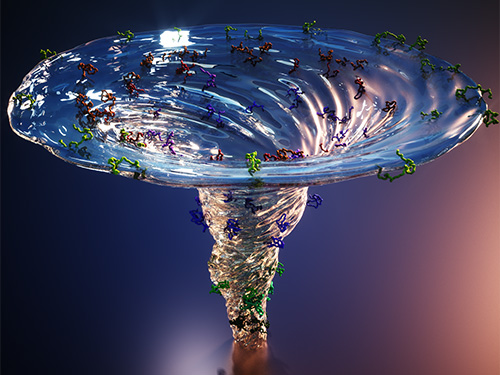
Figure. The scientists found that non-functional unfolded forms of the protein cytochrome c follow different pathways and timelines to reach a stable functional folded state.
Publications:
Kim, T. W., et al. (2020) ‘Protein folding from heterogeneous unfolded state revealed by time-resolved X-ray solution scattering’. PNAS. Volume 117. Issue 26. Page 14996-15005. Available online at https://doi.org/10.1073/pnas.1913442117
Profile: Hyotcherl Ihee, Ph.D.
Professor
hyotcherl.ihee@kaist.ac.kr
http://time.kaist.ac.kr/
Ihee Laboratory
Department of Chemistry
KAIST
https://www.kaist.ac.kr
Daejeon 34141, Korea
Profile: Young Min Rhee, Ph.D.
Professor
ymrhee@kaist.ac.kr
http://singlet.kaist.ac.kr
Rhee Research Group
Department of Chemistry
KAIST
https://www.kaist.ac.kr
Daejeon 34141, Korea
(END)
2020.07.09 View 18070
X-ray Scattering Shines Light on Protein Folding
- Multiple forms of a non-functional, unfolded protein follow different pathways and timelines to reach its folded, functional state, a study reveals. -
KAIST researchers have used an X-ray method to track how proteins fold, which could improve computer simulations of this process, with implications for understanding diseases and improving drug discovery. Their findings were reported in the Proceedings of the National Academy of Sciences of the United States of America (PNAS) on June 30.
When proteins are translated from their DNA codes, they quickly transform from a non-functional, unfolded state into their folded, functional state. Problems in folding can lead to diseases like Alzheimer’s and Parkinson’s.
“Protein folding is one of the most important biological processes, as it forms the functioning 3D protein structure,” explained the physical chemist Hyotcherl Ihee of the Department of Chemistry at KAIST. Dr. Tae Wu Kim, the lead author of this research from Ihee’s group, added, “Understanding the mechanisms of protein folding is important, and could pave the way for disease study and drug development.”
Ihee’s team developed an approach using an X-ray scattering technique to uncover how the protein cytochrome c folds from its initial unfolded state. This protein is composed of a chain of 104 amino acids with an iron-containing heme molecule. It is often used for protein folding studies.
The researchers placed the protein in a solution and shined ultraviolet light on it. This process provides electrons to cytochrome c, reducing the iron within it from the ferric to the ferrous form, which initiates folding. As this was happening, the researchers beamed X-rays at very short intervals onto the sample. The X-rays scattered off all the atomic pairs in the sample and a detector continuously recorded the X-ray scattering patterns. The X-ray scattering patterns provided direct information regarding the 3D protein structure and the changes made in these patterns over time showed real-time motion of the protein during the folding process.
The team found cytochrome c proteins initially exist in a wide variety of unfolded states. Once the folding process is triggered, they stop by a group of intermediates within 31.6 microseconds, and then those intermediates follow different pathways with different folding times to reach an energetically stable folded state.
“We don’t know if this diversity in folding paths can be generalized to other proteins,” Ihee confessed. He continued, “However, we believe that our approach can be used to study other protein folding systems.”
Ihee hopes this approach can improve the accuracy of models that simulate protein interactions by including information on their unstructured states. These simulations are important as they can help identify barriers to proper folding and predict a protein’s folded state given its amino acid sequence. Ultimately, the models could help clarify how some diseases develop and how drugs interact with various protein structures.
Ihee’s group collaborated with Professor Young Min Rhee at the KAIST Department of Chemistry, and this work was supported by the National Research Foundation of Korea (NRF) and the Institute for Basic Science (IBS).
Figure. The scientists found that non-functional unfolded forms of the protein cytochrome c follow different pathways and timelines to reach a stable functional folded state.
Publications:
Kim, T. W., et al. (2020) ‘Protein folding from heterogeneous unfolded state revealed by time-resolved X-ray solution scattering’. PNAS. Volume 117. Issue 26. Page 14996-15005. Available online at https://doi.org/10.1073/pnas.1913442117
Profile: Hyotcherl Ihee, Ph.D.
Professor
hyotcherl.ihee@kaist.ac.kr
http://time.kaist.ac.kr/
Ihee Laboratory
Department of Chemistry
KAIST
https://www.kaist.ac.kr
Daejeon 34141, Korea
Profile: Young Min Rhee, Ph.D.
Professor
ymrhee@kaist.ac.kr
http://singlet.kaist.ac.kr
Rhee Research Group
Department of Chemistry
KAIST
https://www.kaist.ac.kr
Daejeon 34141, Korea
(END)
2020.07.09 View 18070 -
 Every Moment of Ultrafast Chemical Bonding Now Captured on Film
- The emerging moment of bond formation, two separate bonding steps, and subsequent vibrational motions were visualized. -
< Emergence of molecular vibrations and the evolution to covalent bonds observed in the research. Video Credit: KEK IMSS >
A team of South Korean researchers led by Professor Hyotcherl Ihee from the Department of Chemistry at KAIST reported the direct observation of the birthing moment of chemical bonds by tracking real-time atomic positions in the molecule. Professor Ihee, who also serves as Associate Director of the Center for Nanomaterials and Chemical Reactions at the Institute for Basic Science (IBS), conducted this study in collaboration with scientists at the Institute of Materials Structure Science of High Energy Accelerator Research Organization (KEK IMSS, Japan), RIKEN (Japan), and Pohang Accelerator Laboratory (PAL, South Korea). This work was published in Nature on June 24.
Targeted cancer drugs work by striking a tight bond between cancer cell and specific molecular targets that are involved in the growth and spread of cancer. Detailed images of such chemical bonding sites or pathways can provide key information necessary for maximizing the efficacy of oncogene treatments. However, atomic movements in a molecule have never been captured in the middle of the action, not even for an extremely simple molecule such as a triatomic molecule, made of only three atoms.
Professor Ihee's group and their international collaborators finally succeeded in capturing the ongoing reaction process of the chemical bond formation in the gold trimer. "The femtosecond-resolution images revealed that such molecular events took place in two separate stages, not simultaneously as previously assumed," says Professor Ihee, the corresponding author of the study. "The atoms in the gold trimer complex atoms remain in motion even after the chemical bonding is complete. The distance between the atoms increased and decreased periodically, exhibiting the molecular vibration. These visualized molecular vibrations allowed us to name the characteristic motion of each observed vibrational mode." adds Professor Ihee.
Atoms move extremely fast at a scale of femtosecond (fs) ― quadrillionths (or millionths of a billionth) of a second. Its movement is minute in the level of angstrom equal to one ten-billionth of a meter. They are especially elusive during the transition state where reaction intermediates are transitioning from reactants to products in a flash. The KAIST-IBS research team made this experimentally challenging task possible by using femtosecond x-ray liquidography (solution scattering). This experimental technique combines laser photolysis and x-ray scattering techniques. When a laser pulse strikes the sample, X-rays scatter and initiate the chemical bond formation reaction in the gold trimer complex. Femtosecond x-ray pulses obtained from a special light source called an x-ray free-electron laser (XFEL) were used to interrogate the bond-forming process. The experiments were performed at two XFEL facilities (4th generation linear accelerator) that are PAL-XFEL in South Korea and SACLA in Japan, and this study was conducted in collaboration with researchers from KEK IMSS, PAL, RIKEN, and the Japan Synchrotron Radiation Research Institute (JASRI).
Scattered waves from each atom interfere with each other and thus their x-ray scattering images are characterized by specific travel directions. The KAIST-IBS research team traced real-time positions of the three gold atoms over time by analyzing x-ray scattering images, which are determined by a three-dimensional structure of a molecule. Structural changes in the molecule complex resulted in multiple characteristic scattering images over time. When a molecule is excited by a laser pulse, multiple vibrational quantum states are simultaneously excited. The superposition of several excited vibrational quantum states is called a wave packet. The researchers tracked the wave packet in three-dimensional nuclear coordinates and found that the first half round of chemical bonding was formed within 35 fs after photoexcitation. The second half of the reaction followed within 360 fs to complete the entire reaction dynamics.
They also accurately illustrated molecular vibration motions in both temporal- and spatial-wise. This is quite a remarkable feat considering that such an ultrafast speed and a minute length of motion are quite challenging conditions for acquiring precise experimental data.
In this study, the KAIST-IBS research team improved upon their 2015 study published by Nature. In the previous study in 2015, the speed of the x-ray camera (time resolution) was limited to 500 fs, and the molecular structure had already changed to be linear with two chemical bonds within 500 fs. In this study, the progress of the bond formation and bent-to-linear structural transformation could be observed in real time, thanks to the improvement time resolution down to 100 fs. Thereby, the asynchronous bond formation mechanism in which two chemical bonds are formed in 35 fs and 360 fs, respectively, and the bent-to-linear transformation completed in 335 fs were visualized. In short, in addition to observing the beginning and end of chemical reactions, they reported every moment of the intermediate, ongoing rearrangement of nuclear configurations with dramatically improved experimental and analytical methods.
They will push this method of 'real-time tracking of atomic positions in a molecule and molecular vibration using femtosecond x-ray scattering' to reveal the mechanisms of organic and inorganic catalytic reactions and reactions involving proteins in the human body. "By directly tracking the molecular vibrations and real-time positions of all atoms in a molecule in the middle of reaction, we will be able to uncover mechanisms of various unknown organic and inorganic catalytic reactions and biochemical reactions," notes Dr. Jong Goo Kim, the lead author of the study.
Publications:
Kim, J. G., et al. (2020) ‘Mapping the emergence of molecular vibrations mediating bond formation’. Nature. Volume 582. Page 520-524. Available online at https://doi.org/10.1038/s41586-020-2417-3
Profile: Hyotcherl Ihee, Ph.D.
Professor
hyotcherl.ihee@kaist.ac.kr
http://time.kaist.ac.kr/
Ihee Laboratory
Department of Chemistry
KAIST
https://www.kaist.ac.kr
Daejeon 34141, Korea
(END)
2020.06.24 View 21188
Every Moment of Ultrafast Chemical Bonding Now Captured on Film
- The emerging moment of bond formation, two separate bonding steps, and subsequent vibrational motions were visualized. -
< Emergence of molecular vibrations and the evolution to covalent bonds observed in the research. Video Credit: KEK IMSS >
A team of South Korean researchers led by Professor Hyotcherl Ihee from the Department of Chemistry at KAIST reported the direct observation of the birthing moment of chemical bonds by tracking real-time atomic positions in the molecule. Professor Ihee, who also serves as Associate Director of the Center for Nanomaterials and Chemical Reactions at the Institute for Basic Science (IBS), conducted this study in collaboration with scientists at the Institute of Materials Structure Science of High Energy Accelerator Research Organization (KEK IMSS, Japan), RIKEN (Japan), and Pohang Accelerator Laboratory (PAL, South Korea). This work was published in Nature on June 24.
Targeted cancer drugs work by striking a tight bond between cancer cell and specific molecular targets that are involved in the growth and spread of cancer. Detailed images of such chemical bonding sites or pathways can provide key information necessary for maximizing the efficacy of oncogene treatments. However, atomic movements in a molecule have never been captured in the middle of the action, not even for an extremely simple molecule such as a triatomic molecule, made of only three atoms.
Professor Ihee's group and their international collaborators finally succeeded in capturing the ongoing reaction process of the chemical bond formation in the gold trimer. "The femtosecond-resolution images revealed that such molecular events took place in two separate stages, not simultaneously as previously assumed," says Professor Ihee, the corresponding author of the study. "The atoms in the gold trimer complex atoms remain in motion even after the chemical bonding is complete. The distance between the atoms increased and decreased periodically, exhibiting the molecular vibration. These visualized molecular vibrations allowed us to name the characteristic motion of each observed vibrational mode." adds Professor Ihee.
Atoms move extremely fast at a scale of femtosecond (fs) ― quadrillionths (or millionths of a billionth) of a second. Its movement is minute in the level of angstrom equal to one ten-billionth of a meter. They are especially elusive during the transition state where reaction intermediates are transitioning from reactants to products in a flash. The KAIST-IBS research team made this experimentally challenging task possible by using femtosecond x-ray liquidography (solution scattering). This experimental technique combines laser photolysis and x-ray scattering techniques. When a laser pulse strikes the sample, X-rays scatter and initiate the chemical bond formation reaction in the gold trimer complex. Femtosecond x-ray pulses obtained from a special light source called an x-ray free-electron laser (XFEL) were used to interrogate the bond-forming process. The experiments were performed at two XFEL facilities (4th generation linear accelerator) that are PAL-XFEL in South Korea and SACLA in Japan, and this study was conducted in collaboration with researchers from KEK IMSS, PAL, RIKEN, and the Japan Synchrotron Radiation Research Institute (JASRI).
Scattered waves from each atom interfere with each other and thus their x-ray scattering images are characterized by specific travel directions. The KAIST-IBS research team traced real-time positions of the three gold atoms over time by analyzing x-ray scattering images, which are determined by a three-dimensional structure of a molecule. Structural changes in the molecule complex resulted in multiple characteristic scattering images over time. When a molecule is excited by a laser pulse, multiple vibrational quantum states are simultaneously excited. The superposition of several excited vibrational quantum states is called a wave packet. The researchers tracked the wave packet in three-dimensional nuclear coordinates and found that the first half round of chemical bonding was formed within 35 fs after photoexcitation. The second half of the reaction followed within 360 fs to complete the entire reaction dynamics.
They also accurately illustrated molecular vibration motions in both temporal- and spatial-wise. This is quite a remarkable feat considering that such an ultrafast speed and a minute length of motion are quite challenging conditions for acquiring precise experimental data.
In this study, the KAIST-IBS research team improved upon their 2015 study published by Nature. In the previous study in 2015, the speed of the x-ray camera (time resolution) was limited to 500 fs, and the molecular structure had already changed to be linear with two chemical bonds within 500 fs. In this study, the progress of the bond formation and bent-to-linear structural transformation could be observed in real time, thanks to the improvement time resolution down to 100 fs. Thereby, the asynchronous bond formation mechanism in which two chemical bonds are formed in 35 fs and 360 fs, respectively, and the bent-to-linear transformation completed in 335 fs were visualized. In short, in addition to observing the beginning and end of chemical reactions, they reported every moment of the intermediate, ongoing rearrangement of nuclear configurations with dramatically improved experimental and analytical methods.
They will push this method of 'real-time tracking of atomic positions in a molecule and molecular vibration using femtosecond x-ray scattering' to reveal the mechanisms of organic and inorganic catalytic reactions and reactions involving proteins in the human body. "By directly tracking the molecular vibrations and real-time positions of all atoms in a molecule in the middle of reaction, we will be able to uncover mechanisms of various unknown organic and inorganic catalytic reactions and biochemical reactions," notes Dr. Jong Goo Kim, the lead author of the study.
Publications:
Kim, J. G., et al. (2020) ‘Mapping the emergence of molecular vibrations mediating bond formation’. Nature. Volume 582. Page 520-524. Available online at https://doi.org/10.1038/s41586-020-2417-3
Profile: Hyotcherl Ihee, Ph.D.
Professor
hyotcherl.ihee@kaist.ac.kr
http://time.kaist.ac.kr/
Ihee Laboratory
Department of Chemistry
KAIST
https://www.kaist.ac.kr
Daejeon 34141, Korea
(END)
2020.06.24 View 21188 -
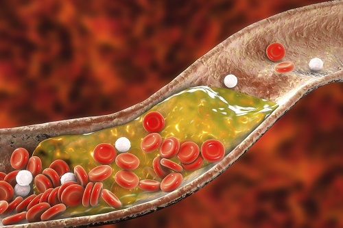 New Nanoparticle Drug Combination For Atherosclerosis
Physicochemical cargo-switching nanoparticles (CSNP) designed by KAIST can help significantly reduce cholesterol and macrophage foam cells in arteries, which are the two main triggers for atherosclerotic plaque and inflammation.
The CSNP-based combination drug delivery therapy was proved to exert cholesterol-lowering, anti-inflammatory, and anti-proliferative functions of two common medications for treating and preventing atherosclerosis that are cyclodextrin and statin. Professor Ji-Ho Park and Dr. Heegon Kim from KAIST’s Department of Bio and Brain Engineering said their study has shown great potential for future applications with reduced side effects.
Atherosclerosis is a chronic inflammatory vascular disease that is characterized by the accumulation of cholesterol and cholesterol-loaded macrophage foam cells in the intima. When this atherosclerotic plaque clogs and narrows the artery walls, they restrict blood flow and cause various cardiovascular conditions such as heart attacks and strokes. Heart attacks and strokes are the world’s first and fifth causes of death respectively.
Oral statin administration has been used in clinics as a standard care for atherosclerosis, which is prescribed to lower blood cholesterol and inhibit its accumulation within the plaque. Although statins can effectively prevent the progression of plaque growth, they have only shown modest efficacy in eliminating the already-established plaque. Therefore, patients are required to take statin drugs for the rest of their lives and will always carry the risk of plaque ruptures that can trigger a blood clot.
To address these issues, Professor Park and Dr. Kim exploited another antiatherogenic agent called cyclodextrin. In their paper published in the Journal of Controlled Release on March 10, Professor Park and Dr. Kim reported that the polymeric formulation of cyclodextrin with a diameter of approximately 10 nanometers(nm) can accumulate within the atherosclerotic plaque 14 times more and effectively reduce the plaque even at lower doses, compared to cyclodextrin in a non-polymer structure.
Moreover, although cyclodextrin is known to have a cytotoxic effect on hair cells in the cochlea, which can lead to hearing loss, cyclodextrin polymers developed by Professor Park’s research group exhibited a varying biodistribution profile and did not have this side effect.
In the follow-up study reported in ACS Nano on April 28, the researchers exploited both cyclodextrin and statin and form the cyclodextrin-statin self-assembly drug complex, based on previous findings that each drug can exert local anti-atherosclerosis effect within the plaque. The complex formation processes were optimized to obtain homogeneous and stable nanoparticles with a diameter of about 100 nm for systematic injection.
The therapeutic synergy of cyclodextrin and statin could reportedly enhance plaque-targeted drug delivery and anti-inflammation. Cyclodextrin led to the regression of cholesterol in the established plaque, and the statins were shown to inhibit the proliferation of macrophage foam cells. The study suggested that combination therapy is required to resolve the complex inflammatory cholesterol-rich microenvironment within the plaque.
Professor Park said, “While nanomedicine has been mainly developed for the treatment of cancers, our studies show that nanomedicine can also play a significant role in treating and preventing atherosclerosis, which causes various cardiovascular diseases that are the leading causes of death worldwide.”
This work was supported by KAIST and the National Research Foundation (NRF) of Korea.
Publications:
1. Heegon Kim, Junhee Han, and Ji-Ho Park. (2020) ‘Cyclodextrin polymer improves atherosclerosis therapy and reduces ototoxicity’ Journal of Controlled Release. Volume 319. Page 77-86. Available online at https://doi.org/10.1016/j.jconrel.2019.12.021
2. Kim, H., et al. (2020) ‘Affinity-Driven Design of Cargo-Switching Nanoparticles to Leverage a Cholesterol-Rich Microenvironment for Atherosclerosis Therapy’ ACS Nano. Available online at https://doi.org/10.1021/acsnano.9b08216
Profile: Ji-Ho Park, Ph.D.
Associate Professor
jihopark@kaist.ac.kr
http://openwetware.org/wiki/Park_Lab
Biomaterials Engineering Laboratory (BEL)
Department of Bio and Brain Engineering (BIOENG)
Korea Advanced Institute of Science and Technology (KAIST)
https://www.kaist.ac.kr
Daejeon 34141, Korea
Profile: Heegon Kim, Ph.D.
Postdoctoral Researcher
heegon@kaist.ac.kr
BEL, BIOENG, KAIST
(END)
2020.06.16 View 16369
New Nanoparticle Drug Combination For Atherosclerosis
Physicochemical cargo-switching nanoparticles (CSNP) designed by KAIST can help significantly reduce cholesterol and macrophage foam cells in arteries, which are the two main triggers for atherosclerotic plaque and inflammation.
The CSNP-based combination drug delivery therapy was proved to exert cholesterol-lowering, anti-inflammatory, and anti-proliferative functions of two common medications for treating and preventing atherosclerosis that are cyclodextrin and statin. Professor Ji-Ho Park and Dr. Heegon Kim from KAIST’s Department of Bio and Brain Engineering said their study has shown great potential for future applications with reduced side effects.
Atherosclerosis is a chronic inflammatory vascular disease that is characterized by the accumulation of cholesterol and cholesterol-loaded macrophage foam cells in the intima. When this atherosclerotic plaque clogs and narrows the artery walls, they restrict blood flow and cause various cardiovascular conditions such as heart attacks and strokes. Heart attacks and strokes are the world’s first and fifth causes of death respectively.
Oral statin administration has been used in clinics as a standard care for atherosclerosis, which is prescribed to lower blood cholesterol and inhibit its accumulation within the plaque. Although statins can effectively prevent the progression of plaque growth, they have only shown modest efficacy in eliminating the already-established plaque. Therefore, patients are required to take statin drugs for the rest of their lives and will always carry the risk of plaque ruptures that can trigger a blood clot.
To address these issues, Professor Park and Dr. Kim exploited another antiatherogenic agent called cyclodextrin. In their paper published in the Journal of Controlled Release on March 10, Professor Park and Dr. Kim reported that the polymeric formulation of cyclodextrin with a diameter of approximately 10 nanometers(nm) can accumulate within the atherosclerotic plaque 14 times more and effectively reduce the plaque even at lower doses, compared to cyclodextrin in a non-polymer structure.
Moreover, although cyclodextrin is known to have a cytotoxic effect on hair cells in the cochlea, which can lead to hearing loss, cyclodextrin polymers developed by Professor Park’s research group exhibited a varying biodistribution profile and did not have this side effect.
In the follow-up study reported in ACS Nano on April 28, the researchers exploited both cyclodextrin and statin and form the cyclodextrin-statin self-assembly drug complex, based on previous findings that each drug can exert local anti-atherosclerosis effect within the plaque. The complex formation processes were optimized to obtain homogeneous and stable nanoparticles with a diameter of about 100 nm for systematic injection.
The therapeutic synergy of cyclodextrin and statin could reportedly enhance plaque-targeted drug delivery and anti-inflammation. Cyclodextrin led to the regression of cholesterol in the established plaque, and the statins were shown to inhibit the proliferation of macrophage foam cells. The study suggested that combination therapy is required to resolve the complex inflammatory cholesterol-rich microenvironment within the plaque.
Professor Park said, “While nanomedicine has been mainly developed for the treatment of cancers, our studies show that nanomedicine can also play a significant role in treating and preventing atherosclerosis, which causes various cardiovascular diseases that are the leading causes of death worldwide.”
This work was supported by KAIST and the National Research Foundation (NRF) of Korea.
Publications:
1. Heegon Kim, Junhee Han, and Ji-Ho Park. (2020) ‘Cyclodextrin polymer improves atherosclerosis therapy and reduces ototoxicity’ Journal of Controlled Release. Volume 319. Page 77-86. Available online at https://doi.org/10.1016/j.jconrel.2019.12.021
2. Kim, H., et al. (2020) ‘Affinity-Driven Design of Cargo-Switching Nanoparticles to Leverage a Cholesterol-Rich Microenvironment for Atherosclerosis Therapy’ ACS Nano. Available online at https://doi.org/10.1021/acsnano.9b08216
Profile: Ji-Ho Park, Ph.D.
Associate Professor
jihopark@kaist.ac.kr
http://openwetware.org/wiki/Park_Lab
Biomaterials Engineering Laboratory (BEL)
Department of Bio and Brain Engineering (BIOENG)
Korea Advanced Institute of Science and Technology (KAIST)
https://www.kaist.ac.kr
Daejeon 34141, Korea
Profile: Heegon Kim, Ph.D.
Postdoctoral Researcher
heegon@kaist.ac.kr
BEL, BIOENG, KAIST
(END)
2020.06.16 View 16369 -
 Professor Jee-Hwan Ryu Receives IEEE ICRA 2020 Outstanding Reviewer Award
Professor Jee-Hwan Ryu from the Department of Civil and Environmental Engineering was selected as this year’s winner of the Outstanding Reviewer Award presented by the Institute of Electrical and Electronics Engineers International Conference on Robotics and Automation (IEEE ICRA). The award ceremony took place on June 5 during the conference that is being held online May 31 through August 31 for three months.
The IEEE ICRA Outstanding Reviewer Award is given every year to the top reviewers who have provided constructive and high-quality thesis reviews, and contributed to improving the quality of papers published as results of the conference.
Professor Ryu was one of the four winners of this year’s award. He was selected from 9,425 candidates, which was approximately three times bigger than the candidate pool in previous years. He was strongly recommended by the editorial committee of the conference.
(END)
2020.06.10 View 11766
Professor Jee-Hwan Ryu Receives IEEE ICRA 2020 Outstanding Reviewer Award
Professor Jee-Hwan Ryu from the Department of Civil and Environmental Engineering was selected as this year’s winner of the Outstanding Reviewer Award presented by the Institute of Electrical and Electronics Engineers International Conference on Robotics and Automation (IEEE ICRA). The award ceremony took place on June 5 during the conference that is being held online May 31 through August 31 for three months.
The IEEE ICRA Outstanding Reviewer Award is given every year to the top reviewers who have provided constructive and high-quality thesis reviews, and contributed to improving the quality of papers published as results of the conference.
Professor Ryu was one of the four winners of this year’s award. He was selected from 9,425 candidates, which was approximately three times bigger than the candidate pool in previous years. He was strongly recommended by the editorial committee of the conference.
(END)
2020.06.10 View 11766 -
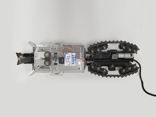 ‘Mole-bot’ Optimized for Underground and Space Exploration
Biomimetic drilling robot provides new insights into the development of efficient drilling technologies
Mole-bot, a drilling biomimetic robot designed by KAIST, boasts a stout scapula, a waist inclinable on all sides, and powerful forelimbs. Most of all, the powerful torque from the expandable drilling bit mimicking the chiseling ability of a mole’s front teeth highlights the best feature of the drilling robot.
The Mole-bot is expected to be used for space exploration and mining for underground resources such as coalbed methane and Rare Earth Elements (REE), which require highly advanced drilling technologies in complex environments.
The research team, led by Professor Hyun Myung from the School of Electrical Engineering, found inspiration for their drilling bot from two striking features of the African mole-rat and European mole.
“The crushing power of the African mole-rat’s teeth is so powerful that they can dig a hole with 48 times more power than their body weight. We used this characteristic for building the main excavation tool. And its expandable drill is designed not to collide with its forelimbs,” said Professor Myung.
The 25-cm wide and 84-cm long Mole-bot can excavate three times faster with six times higher directional accuracy than conventional models. The Mole-bot weighs 26 kg.
After digging, the robot removes the excavated soil and debris using its forelimbs. This embedded muscle feature, inspired by the European mole’s scapula, converts linear motion into a powerful rotational force. For directional drilling, the robot’s elongated waist changes its direction 360° like living mammals.
For exploring underground environments, the research team developed and applied new sensor systems and algorithms to identify the robot’s position and orientation using graph-based 3D Simultaneous Localization and Mapping (SLAM) technology that matches the Earth’s magnetic field sequence, which enables 3D autonomous navigation underground.
According to Market & Market’s survey, the directional drilling market in 2016 is estimated to be 83.3 billion USD and is expected to grow to 103 billion USD in 2021. The growth of the drilling market, starting with the Shale Revolution, is likely to expand into the future development of space and polar resources. As initiated by Space X recently, more attention for planetary exploration will be on the rise and its related technology and equipment market will also increase.
The Mole-bot is a huge step forward for efficient underground drilling and exploration technologies. Unlike conventional drilling processes that use environmentally unfriendly mud compounds for cleaning debris, Mole-bot can mitigate environmental destruction. The researchers said their system saves on cost and labor and does not require additional pipelines or other ancillary equipment.
“We look forward to a more efficient resource exploration with this type of drilling robot. We also hope Mole-bot will have a very positive impact on the robotics market in terms of its extensive application spectra and economic feasibility,” said Professor Myung.
This research, made in collaboration with Professor Jung-Wuk Hong and Professor Tae-Hyuk Kwon’s team in the Department of Civil and Environmental Engineering for robot structure analysis and geotechnical experiments, was supported by the Ministry of Trade, Industry and Energy’s Industrial Technology Innovation Project.
Profile
Professor Hyun Myung
Urban Robotics Lab
http://urobot.kaist.ac.kr/
School of Electrical Engineering
KAIST
2020.06.05 View 13210
‘Mole-bot’ Optimized for Underground and Space Exploration
Biomimetic drilling robot provides new insights into the development of efficient drilling technologies
Mole-bot, a drilling biomimetic robot designed by KAIST, boasts a stout scapula, a waist inclinable on all sides, and powerful forelimbs. Most of all, the powerful torque from the expandable drilling bit mimicking the chiseling ability of a mole’s front teeth highlights the best feature of the drilling robot.
The Mole-bot is expected to be used for space exploration and mining for underground resources such as coalbed methane and Rare Earth Elements (REE), which require highly advanced drilling technologies in complex environments.
The research team, led by Professor Hyun Myung from the School of Electrical Engineering, found inspiration for their drilling bot from two striking features of the African mole-rat and European mole.
“The crushing power of the African mole-rat’s teeth is so powerful that they can dig a hole with 48 times more power than their body weight. We used this characteristic for building the main excavation tool. And its expandable drill is designed not to collide with its forelimbs,” said Professor Myung.
The 25-cm wide and 84-cm long Mole-bot can excavate three times faster with six times higher directional accuracy than conventional models. The Mole-bot weighs 26 kg.
After digging, the robot removes the excavated soil and debris using its forelimbs. This embedded muscle feature, inspired by the European mole’s scapula, converts linear motion into a powerful rotational force. For directional drilling, the robot’s elongated waist changes its direction 360° like living mammals.
For exploring underground environments, the research team developed and applied new sensor systems and algorithms to identify the robot’s position and orientation using graph-based 3D Simultaneous Localization and Mapping (SLAM) technology that matches the Earth’s magnetic field sequence, which enables 3D autonomous navigation underground.
According to Market & Market’s survey, the directional drilling market in 2016 is estimated to be 83.3 billion USD and is expected to grow to 103 billion USD in 2021. The growth of the drilling market, starting with the Shale Revolution, is likely to expand into the future development of space and polar resources. As initiated by Space X recently, more attention for planetary exploration will be on the rise and its related technology and equipment market will also increase.
The Mole-bot is a huge step forward for efficient underground drilling and exploration technologies. Unlike conventional drilling processes that use environmentally unfriendly mud compounds for cleaning debris, Mole-bot can mitigate environmental destruction. The researchers said their system saves on cost and labor and does not require additional pipelines or other ancillary equipment.
“We look forward to a more efficient resource exploration with this type of drilling robot. We also hope Mole-bot will have a very positive impact on the robotics market in terms of its extensive application spectra and economic feasibility,” said Professor Myung.
This research, made in collaboration with Professor Jung-Wuk Hong and Professor Tae-Hyuk Kwon’s team in the Department of Civil and Environmental Engineering for robot structure analysis and geotechnical experiments, was supported by the Ministry of Trade, Industry and Energy’s Industrial Technology Innovation Project.
Profile
Professor Hyun Myung
Urban Robotics Lab
http://urobot.kaist.ac.kr/
School of Electrical Engineering
KAIST
2020.06.05 View 13210 -
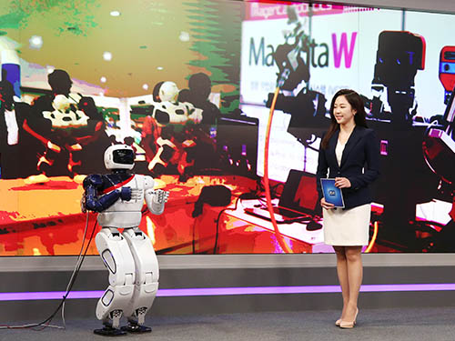 Hubo Debuts as a News Anchor
HUBO, a humanoid robot developed by Professor Jun-Ho Oh’s team, made its debut as a co-anchor during the TJB prime time news 8 on May 14.
“Un-contact" became the new normal after Covid-19 and many business solutions are being transformed using robotics. HUBO made two news reports on contactless services using robots in medical, manufacturing, and logistics industries. HUBO 2, the second generation of HUBO, appeared as a special anchor on the local broadcasting network’s special program in celebration of its 25th anniversary.
HUBO is the champion of the 2015 DARPA Robotics Challenge held in the USA. Its FX-2 riding robot also participated in the Olympic torch relay during the 2018 PyeongChang Winter Olympics.
Click here to watch a full video of HUBO anchoring the news.
(END)
2020.05.14 View 14806
Hubo Debuts as a News Anchor
HUBO, a humanoid robot developed by Professor Jun-Ho Oh’s team, made its debut as a co-anchor during the TJB prime time news 8 on May 14.
“Un-contact" became the new normal after Covid-19 and many business solutions are being transformed using robotics. HUBO made two news reports on contactless services using robots in medical, manufacturing, and logistics industries. HUBO 2, the second generation of HUBO, appeared as a special anchor on the local broadcasting network’s special program in celebration of its 25th anniversary.
HUBO is the champion of the 2015 DARPA Robotics Challenge held in the USA. Its FX-2 riding robot also participated in the Olympic torch relay during the 2018 PyeongChang Winter Olympics.
Click here to watch a full video of HUBO anchoring the news.
(END)
2020.05.14 View 14806 -
 Highly Efficient and Stable Double Layer Solar Cell Developed
Solar cells convert light into energy, but they can be inefficient and vulnerable to the environment, degrading with, ironically, too much light or other factors, including moisture and low temperature. An international research team has developed a new type of solar cell that can both withstand environmental hazards and is 26.7% efficient in power conversion.
They published their results on March 26 in Science.
The researchers, led by Byungha Shin, a professor from the Department of Materials Science and Engineering at KAIST, focused on developing a new class of light-absorbing material, called a wide bandgap perovskite. The material has a highly effective crystal structure that can process the power needs, but it can become problematic when exposed to environmental hazards, such as moisture. Researchers have made some progress increasing the efficiency of solar cells based on perovskite, but the material has greater potential than what was previously achieved.
To achieve better performance, Shin and his team built a double layer solar cell, called tandem, in which two or more light absorbers are stacked together to better utilize solar energy. To use perovskite in these tandem devices, the scientists modified the material’s optical property, which allows it to absorb a wider range of solar energy. Without the adjustment, the material is not as useful in achieving high performing tandem solar cells. The modification of the optical property of perovskite, however, comes with a penalty — the material becomes hugely vulnerable to the environment, in particular, to light.
To counteract the wide bandgap perovskite’s delicate nature, the researchers engineered combinations of molecules composing a two-dimensional layer in the perovskite, stabilizing the solar cells.
“We developed a high-quality wide bandgap perovskite material and, in combination with silicon solar cells, achieved world-class perovskite-silicon tandem cells,” Shin said.
The development was only possible due to the engineering method, in which the mixing ratio of the molecules building the two-dimensional layer are carefully controlled. In this case, the perovskite material not only improved efficiency of the resulting solar cell but also gained durability, retaining 80% of its initial power conversion capability even after 1,000 hours of continuous illumination. This is the first time such a high efficiency has been achieved with a wide bandgap perovskite single layer alone, according to Shin.
“Such high-efficiency wide bandgap perovskite is an essential technology for achieving ultra-high efficiency of perovskite-silicon tandem (double layer) solar cells,” Shin said. “The results also show the importance of bandgap matching of upper and lower cells in these tandem solar cells.”
The researchers, having stabilized the wide bandgap perovskite material, are now focused on developing even more efficient tandem solar cells that are expected to have more than 30% of power conversion efficiency, something that no one has achieved yet,
“Our ultimate goal is to develop ultra-high-efficiency tandem solar cells that contribute to the increase of shared solar energy among all energy sources,” Shin said. “We want to contribute to making the planet healthier.”
This work was supported by the National Research Foundation of Korea, the Korea Institute of Energy Technology Evaluation and Planning, the Ministry of Trade Industry and Energy of Korea, and the U.S. Department of Energy.
Other contributors include Daehan Kim, Jekyung Kim, Passarut Boonmongkolras, Seong Ryul Pae and Minkyu Kim, all of whom affiliated with the Department of Materials Science and Engineering at KAIST. Other authors include Byron W. Larson, Sean P. Dunfield, Chuanxiao Xiao, Jinhui Tong, Fei Zhang, Joseph J. Berry, Kai Zhu and Dong Hoe Kim, all of who are affiliated with the National Renewable Energy Laboratory in Colorado. Dunfield is also affiliated with the Materials Science and Engineering Program at the University of Colorado; Berry is also affiliated with the Department of Physics and the Renewable and Sustainable Energy Institute at the University of Colorado Boulder; and Kim is also affiliated with the Department of Nanotechnology and Advanced Materials Engineering at Sejong University. Hee Joon Jung and Vinayak Dravid of the Department of Materials Science and Engineering at Northwestern University; Ik Jae Park, Su Geun Ji and Jin Young Kim of the Department of Materials Science and Engineering at Seoul National University; and Seok Beom Kang of the Department of Nanotechnology and Advanced Materials Engineering of Sejong University also contributed.
Image credit: Professor Byungha Shin, KAIST
Image usage restrictions: News organizations may use or redistribute this image, with proper attribution, as part of news coverage of this paper only.
Publication: Kim et al. (2020) “Efficient, stable silicon tandem cells enabled by anion-engineered wide band gap perovskites”. Science. Available online at https://doi.org/10.1126/science.aba3433
Profile:
Byungha Shin
Professor
byungha@kaist.ac.kr
http://energymatlab.kaist.ac.kr/
Department of Materials Science and Engineering
KAIST
Profile:
Daehan Kim
Ph.D. Candidate
zxzx4592@kaist.ac.kr
http://energymatlab.kaist.ac.kr/
Department of Materials Science and Engineering
KAIST
(END)
2020.03.27 View 24551
Highly Efficient and Stable Double Layer Solar Cell Developed
Solar cells convert light into energy, but they can be inefficient and vulnerable to the environment, degrading with, ironically, too much light or other factors, including moisture and low temperature. An international research team has developed a new type of solar cell that can both withstand environmental hazards and is 26.7% efficient in power conversion.
They published their results on March 26 in Science.
The researchers, led by Byungha Shin, a professor from the Department of Materials Science and Engineering at KAIST, focused on developing a new class of light-absorbing material, called a wide bandgap perovskite. The material has a highly effective crystal structure that can process the power needs, but it can become problematic when exposed to environmental hazards, such as moisture. Researchers have made some progress increasing the efficiency of solar cells based on perovskite, but the material has greater potential than what was previously achieved.
To achieve better performance, Shin and his team built a double layer solar cell, called tandem, in which two or more light absorbers are stacked together to better utilize solar energy. To use perovskite in these tandem devices, the scientists modified the material’s optical property, which allows it to absorb a wider range of solar energy. Without the adjustment, the material is not as useful in achieving high performing tandem solar cells. The modification of the optical property of perovskite, however, comes with a penalty — the material becomes hugely vulnerable to the environment, in particular, to light.
To counteract the wide bandgap perovskite’s delicate nature, the researchers engineered combinations of molecules composing a two-dimensional layer in the perovskite, stabilizing the solar cells.
“We developed a high-quality wide bandgap perovskite material and, in combination with silicon solar cells, achieved world-class perovskite-silicon tandem cells,” Shin said.
The development was only possible due to the engineering method, in which the mixing ratio of the molecules building the two-dimensional layer are carefully controlled. In this case, the perovskite material not only improved efficiency of the resulting solar cell but also gained durability, retaining 80% of its initial power conversion capability even after 1,000 hours of continuous illumination. This is the first time such a high efficiency has been achieved with a wide bandgap perovskite single layer alone, according to Shin.
“Such high-efficiency wide bandgap perovskite is an essential technology for achieving ultra-high efficiency of perovskite-silicon tandem (double layer) solar cells,” Shin said. “The results also show the importance of bandgap matching of upper and lower cells in these tandem solar cells.”
The researchers, having stabilized the wide bandgap perovskite material, are now focused on developing even more efficient tandem solar cells that are expected to have more than 30% of power conversion efficiency, something that no one has achieved yet,
“Our ultimate goal is to develop ultra-high-efficiency tandem solar cells that contribute to the increase of shared solar energy among all energy sources,” Shin said. “We want to contribute to making the planet healthier.”
This work was supported by the National Research Foundation of Korea, the Korea Institute of Energy Technology Evaluation and Planning, the Ministry of Trade Industry and Energy of Korea, and the U.S. Department of Energy.
Other contributors include Daehan Kim, Jekyung Kim, Passarut Boonmongkolras, Seong Ryul Pae and Minkyu Kim, all of whom affiliated with the Department of Materials Science and Engineering at KAIST. Other authors include Byron W. Larson, Sean P. Dunfield, Chuanxiao Xiao, Jinhui Tong, Fei Zhang, Joseph J. Berry, Kai Zhu and Dong Hoe Kim, all of who are affiliated with the National Renewable Energy Laboratory in Colorado. Dunfield is also affiliated with the Materials Science and Engineering Program at the University of Colorado; Berry is also affiliated with the Department of Physics and the Renewable and Sustainable Energy Institute at the University of Colorado Boulder; and Kim is also affiliated with the Department of Nanotechnology and Advanced Materials Engineering at Sejong University. Hee Joon Jung and Vinayak Dravid of the Department of Materials Science and Engineering at Northwestern University; Ik Jae Park, Su Geun Ji and Jin Young Kim of the Department of Materials Science and Engineering at Seoul National University; and Seok Beom Kang of the Department of Nanotechnology and Advanced Materials Engineering of Sejong University also contributed.
Image credit: Professor Byungha Shin, KAIST
Image usage restrictions: News organizations may use or redistribute this image, with proper attribution, as part of news coverage of this paper only.
Publication: Kim et al. (2020) “Efficient, stable silicon tandem cells enabled by anion-engineered wide band gap perovskites”. Science. Available online at https://doi.org/10.1126/science.aba3433
Profile:
Byungha Shin
Professor
byungha@kaist.ac.kr
http://energymatlab.kaist.ac.kr/
Department of Materials Science and Engineering
KAIST
Profile:
Daehan Kim
Ph.D. Candidate
zxzx4592@kaist.ac.kr
http://energymatlab.kaist.ac.kr/
Department of Materials Science and Engineering
KAIST
(END)
2020.03.27 View 24551 -
 Ultrathin but Fully Packaged High-Resolution Camera
- Biologically inspired ultrathin arrayed camera captures super-resolution images. -
The unique structures of biological vision systems in nature inspired scientists to design ultracompact imaging systems. A research group led by Professor Ki-Hun Jeong have made an ultracompact camera that captures high-contrast and high-resolution images. Fully packaged with micro-optical elements such as inverted micro-lenses, multilayered pinhole arrays, and gap spacers on the image sensor, the camera boasts a total track length of 740 μm and a field of view of 73°.
Inspired by the eye structures of the paper wasp species Xenos peckii, the research team completely suppressed optical noise between micro-lenses while reducing camera thickness. The camera has successfully demonstrated high-contrast clear array images acquired from tiny micro lenses. To further enhance the image quality of the captured image, the team combined the arrayed images into one image through super-resolution imaging.
An insect’s compound eye has superior visual characteristics, such as a wide viewing angle, high motion sensitivity, and a large depth of field while maintaining a small volume of visual structure with a small focal length. Among them, the eyes of Xenos peckii and an endoparasite found on paper wasps have hundreds of photoreceptors in a single lens unlike conventional compound eyes. In particular, the eye structures of an adult Xenos peckii exhibit hundreds of photoreceptors on an individual eyelet and offer engineering inspiration for ultrathin cameras or imaging applications because they have higher visual acuity than other compound eyes.
For instance, Xenos peckii’s eye-inspired cameras provide a 50 times higher spatial resolution than those based on arthropod eyes. In addition, the effective image resolution of the Xenos peckii’s eye can be further improved using the image overlaps between neighboring eyelets. This unique structure offers higher visual resolution than other insect eyes.
The team achieved high-contrast and super-resolution imaging through a novel arrayed design of micro-optical elements comprising multilayered aperture arrays and inverted micro-lens arrays directly stacked over an image sensor. This optical component was integrated with a complementary metal oxide semiconductor image sensor.
This is first demonstration of super-resolution imaging which acquires a single integrated image with high contrast and high resolving power reconstructed from high-contrast array images. It is expected that this ultrathin arrayed camera can be applied for further developing mobile devices, advanced surveillance vehicles, and endoscopes.
Professor Jeong said, “This research has led to technological advances in imaging technology. We will continue to strive to make significant impacts on multidisciplinary research projects in the fields of microtechnology and nanotechnology, seeking inspiration from natural photonic structures.”
This work was featured in Light Science & Applications last month and was supported by the National Research Foundation (NRF) of and the Ministry of Health and Welfare (MOHW) of Korea.
Image credit: Professor Ki-Hun Jeong, KAIST
Image usage restrictions: News organizations may use or redistribute this image, with proper attribution, as part of news coverage of this paper only.
Publication:
Kisoo Kim, Kyung-Won Jang, Jae-Kwan Ryu, and Ki-Hun Jeong. (2020) “Biologically inspired ultrathin arrayed camera for high-contrast and high-resolution imaging”. Light Science & Applications. Volume 9. Article 28. Available online at https://doi.org/10.1038/s41377-020-0261-8
Profile:
Ki-Hun Jeong
Professor
kjeong@kaist.ac.kr
http://biophotonics.kaist.ac.kr/
Department of Bio and Brain Engineering
KAIST
Profile:
Kisoo Kim
Ph.D. Candidate
kisoo.kim1@kaist.ac.kr
http://biophotonics.kaist.ac.kr/
Department of Bio and Brain Engineering
KAIST
(END)
2020.03.23 View 22334
Ultrathin but Fully Packaged High-Resolution Camera
- Biologically inspired ultrathin arrayed camera captures super-resolution images. -
The unique structures of biological vision systems in nature inspired scientists to design ultracompact imaging systems. A research group led by Professor Ki-Hun Jeong have made an ultracompact camera that captures high-contrast and high-resolution images. Fully packaged with micro-optical elements such as inverted micro-lenses, multilayered pinhole arrays, and gap spacers on the image sensor, the camera boasts a total track length of 740 μm and a field of view of 73°.
Inspired by the eye structures of the paper wasp species Xenos peckii, the research team completely suppressed optical noise between micro-lenses while reducing camera thickness. The camera has successfully demonstrated high-contrast clear array images acquired from tiny micro lenses. To further enhance the image quality of the captured image, the team combined the arrayed images into one image through super-resolution imaging.
An insect’s compound eye has superior visual characteristics, such as a wide viewing angle, high motion sensitivity, and a large depth of field while maintaining a small volume of visual structure with a small focal length. Among them, the eyes of Xenos peckii and an endoparasite found on paper wasps have hundreds of photoreceptors in a single lens unlike conventional compound eyes. In particular, the eye structures of an adult Xenos peckii exhibit hundreds of photoreceptors on an individual eyelet and offer engineering inspiration for ultrathin cameras or imaging applications because they have higher visual acuity than other compound eyes.
For instance, Xenos peckii’s eye-inspired cameras provide a 50 times higher spatial resolution than those based on arthropod eyes. In addition, the effective image resolution of the Xenos peckii’s eye can be further improved using the image overlaps between neighboring eyelets. This unique structure offers higher visual resolution than other insect eyes.
The team achieved high-contrast and super-resolution imaging through a novel arrayed design of micro-optical elements comprising multilayered aperture arrays and inverted micro-lens arrays directly stacked over an image sensor. This optical component was integrated with a complementary metal oxide semiconductor image sensor.
This is first demonstration of super-resolution imaging which acquires a single integrated image with high contrast and high resolving power reconstructed from high-contrast array images. It is expected that this ultrathin arrayed camera can be applied for further developing mobile devices, advanced surveillance vehicles, and endoscopes.
Professor Jeong said, “This research has led to technological advances in imaging technology. We will continue to strive to make significant impacts on multidisciplinary research projects in the fields of microtechnology and nanotechnology, seeking inspiration from natural photonic structures.”
This work was featured in Light Science & Applications last month and was supported by the National Research Foundation (NRF) of and the Ministry of Health and Welfare (MOHW) of Korea.
Image credit: Professor Ki-Hun Jeong, KAIST
Image usage restrictions: News organizations may use or redistribute this image, with proper attribution, as part of news coverage of this paper only.
Publication:
Kisoo Kim, Kyung-Won Jang, Jae-Kwan Ryu, and Ki-Hun Jeong. (2020) “Biologically inspired ultrathin arrayed camera for high-contrast and high-resolution imaging”. Light Science & Applications. Volume 9. Article 28. Available online at https://doi.org/10.1038/s41377-020-0261-8
Profile:
Ki-Hun Jeong
Professor
kjeong@kaist.ac.kr
http://biophotonics.kaist.ac.kr/
Department of Bio and Brain Engineering
KAIST
Profile:
Kisoo Kim
Ph.D. Candidate
kisoo.kim1@kaist.ac.kr
http://biophotonics.kaist.ac.kr/
Department of Bio and Brain Engineering
KAIST
(END)
2020.03.23 View 22334