Ro
-
 An Improved Carbon Nanotube Semiconductor
Professor Yang-Kyu Choi and his research team of the School of Electrical Engineering at KAIST collaborated with Professor Sung-Jin Choi of Kookmin University to develop a large-scale carbon nanotube semiconductor by using a 3-D fin-gate structure with carbon nanotubes on its top.
Dong Il Lee, a postdoctoral researcher at KAIST’s Electrical Engineering School, participated in this study as the first author. It was published in ACS Nano on November 10, 2016, and was entitled “Three-Dimensional Fin-Structured Semiconducting Carbon Nanotube Network Transistor.”
A semiconductor made with carbon nanotubes operates faster than a silicon semiconductor and requires less energy, yielding higher performance.
Most electronic equipment and devices, however, use silicon semiconductors because it is difficult to fabricate highly purified and densely packed semiconductors with carbon nanotubes (CNTs).
To date, the performance of CNTs was limited due to their low density. Their purity was also low, so it was impossible to make products that had a constant yield on a large-surface wafer or substrate. These characteristics made the mass production of semiconducting CNTs difficult.
To solve these difficulties, the research team used a 3-D fin-gate to vapor-deposit carbon nanotubes on its top. They developed a semiconductor that had a high current density with a width less than 50 nm.
The three-dimensional fin structure was able to vapor-deposit 600 carbon nanotubes per micrometer. This structure could have 20 times more nanotubes than the two dimensional structure, which could only vapor-deposit thirty in the same 1 micrometer width.
In addition, the research team used semi-conductive carbon nanotubes having a purity rating higher than 99.9% from a previous study to obtain a high yield semiconductor.
The semiconductor from the research group has a high current density even with a width less than 50 μm. The new semiconductor is expected to be five times faster than a silicon-based semiconductor and will require five times less electricity during operation.
Furthermore, the new semiconductor can be made by or will be compatible with the equipment for producing silicon-based semiconductors, so there will be no additional costs.
Researcher Lee said, “As a next generation semiconductor, the carbon nanotube semiconductor will have better performance, and its effectiveness will be higher.” He also added, “Hopefully, the new semiconductor will replace the silicon-based semiconductors in ten years.”
This study received support from the Center for Integrated Smart Sensors funded by the Ministry of Science, ICT & Future Planning of Korea as the Global Frontier Project, and from the CMOS (Complementary Metal-Oxide-Semiconductor) THz Technology Convergence Center of the Pioneer Research Center Program sponsored by the National Research Foundation of Korea.
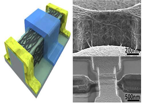
Picture 1: 3D Diagram of the Carbon Nanotube Electronic Device and Its Scanning Electron Microscope (SEM) Image
Picture 2: 3D Transistor Device on an 8-inch Base and the SEM Image of Its Cross Section
2017.02.16 View 12779
An Improved Carbon Nanotube Semiconductor
Professor Yang-Kyu Choi and his research team of the School of Electrical Engineering at KAIST collaborated with Professor Sung-Jin Choi of Kookmin University to develop a large-scale carbon nanotube semiconductor by using a 3-D fin-gate structure with carbon nanotubes on its top.
Dong Il Lee, a postdoctoral researcher at KAIST’s Electrical Engineering School, participated in this study as the first author. It was published in ACS Nano on November 10, 2016, and was entitled “Three-Dimensional Fin-Structured Semiconducting Carbon Nanotube Network Transistor.”
A semiconductor made with carbon nanotubes operates faster than a silicon semiconductor and requires less energy, yielding higher performance.
Most electronic equipment and devices, however, use silicon semiconductors because it is difficult to fabricate highly purified and densely packed semiconductors with carbon nanotubes (CNTs).
To date, the performance of CNTs was limited due to their low density. Their purity was also low, so it was impossible to make products that had a constant yield on a large-surface wafer or substrate. These characteristics made the mass production of semiconducting CNTs difficult.
To solve these difficulties, the research team used a 3-D fin-gate to vapor-deposit carbon nanotubes on its top. They developed a semiconductor that had a high current density with a width less than 50 nm.
The three-dimensional fin structure was able to vapor-deposit 600 carbon nanotubes per micrometer. This structure could have 20 times more nanotubes than the two dimensional structure, which could only vapor-deposit thirty in the same 1 micrometer width.
In addition, the research team used semi-conductive carbon nanotubes having a purity rating higher than 99.9% from a previous study to obtain a high yield semiconductor.
The semiconductor from the research group has a high current density even with a width less than 50 μm. The new semiconductor is expected to be five times faster than a silicon-based semiconductor and will require five times less electricity during operation.
Furthermore, the new semiconductor can be made by or will be compatible with the equipment for producing silicon-based semiconductors, so there will be no additional costs.
Researcher Lee said, “As a next generation semiconductor, the carbon nanotube semiconductor will have better performance, and its effectiveness will be higher.” He also added, “Hopefully, the new semiconductor will replace the silicon-based semiconductors in ten years.”
This study received support from the Center for Integrated Smart Sensors funded by the Ministry of Science, ICT & Future Planning of Korea as the Global Frontier Project, and from the CMOS (Complementary Metal-Oxide-Semiconductor) THz Technology Convergence Center of the Pioneer Research Center Program sponsored by the National Research Foundation of Korea.
Picture 1: 3D Diagram of the Carbon Nanotube Electronic Device and Its Scanning Electron Microscope (SEM) Image
Picture 2: 3D Transistor Device on an 8-inch Base and the SEM Image of Its Cross Section
2017.02.16 View 12779 -
 Controlling DNA Orientation Using a Brush
Professor Dong Ki Yoon’s research team in the Graduate School of Nanoscience and Technology has developed a technique for producing periodic DNA zigzag structures using a common make-up brush.
The results of the research, first-authored by Ph.D. student Yun Jeong Cha and published in Advanced Materials (online, November 15, 2016), has been highlighted in the hot topics of “Liquid Crystals.”
There exist various methods for synthesizing DNA-based nanostructures, but they commonly involved complex design processes and required expensive DNA samples with regulated base sequences.
Using DNA materials extracted from salmon, the research team was able to produce a nanostructure with a well-aligned zigzag pattern at one-thousandth of the usual cost.
The team used a commercial make-up brush bought at a cosmetics store, and with it, applied the salmon DNA in one direction onto a plate, in the same way paint is brushed onto paper. Using a brush with a width of several centimeters, the team aligned DNA molecules of 2 nanometers in diameter along the direction of the brush strokes.
As the thin and dense film of DNA came into contact with air, it lost moisture. An expansive force was created between the dried film and the plate. This force interacted with the elastic force of DNA and caused undulations in the uni-directionally aligned DNA molecules, which resulted in a regular zigzag pattern.
The zigzag DNA’s base sequences could not be controlled because it was extracted from biological sources. However, it has the advantage of being cheap and readily available without compromising its structural integrity and provides a very regular and intricate structure.
This kind of well-ordered DNA structure can be used as template because it can guide or control versatile guest functional materials that are applied to its surface. For example, it can align liquid crystals used in displays, as well as metallic particles and semi-conductors. It is expected that this capacity can be extended to optoelectric devices in the future.
Professor Yoon remarked that “these findings have special implications, as they have demonstrated that various materials in nature aside from DNA, such as proteins, muscle cells, and components of bones can be applied to optoelectric devices.”
This research has been carried out with the support of the Korea National Research Foundation’s Nanomaterials Fundamental Technology Development Program and the Pioneer Research Center under the High-tech Convergence Technology Development Program.
Source: "Control of Periodic Zigzag Structures of DNA by a Simple Shearing Method" by Yun Jeong Cha and Dong Ki Yoon (Advanced Materials, November 15, 2016, DOI: 10.1002/adma.201604247)
Figure 1. Diagram showing the well-ordered zigzag structure of DNA, and the internal molecular orientation
Figure 2. (Left) Unaligned DNA (Right) Aligned DNA after being brushed and dried
Figure 3. Control of the periodicity of the DNA zigzag patterns using micro-channel plates
Figure 4. Diagram representing the control of orientation of liquid crystal materials applied on a zigzag DNA template, and a polarized optical microscope image
2017.01.10 View 7339
Controlling DNA Orientation Using a Brush
Professor Dong Ki Yoon’s research team in the Graduate School of Nanoscience and Technology has developed a technique for producing periodic DNA zigzag structures using a common make-up brush.
The results of the research, first-authored by Ph.D. student Yun Jeong Cha and published in Advanced Materials (online, November 15, 2016), has been highlighted in the hot topics of “Liquid Crystals.”
There exist various methods for synthesizing DNA-based nanostructures, but they commonly involved complex design processes and required expensive DNA samples with regulated base sequences.
Using DNA materials extracted from salmon, the research team was able to produce a nanostructure with a well-aligned zigzag pattern at one-thousandth of the usual cost.
The team used a commercial make-up brush bought at a cosmetics store, and with it, applied the salmon DNA in one direction onto a plate, in the same way paint is brushed onto paper. Using a brush with a width of several centimeters, the team aligned DNA molecules of 2 nanometers in diameter along the direction of the brush strokes.
As the thin and dense film of DNA came into contact with air, it lost moisture. An expansive force was created between the dried film and the plate. This force interacted with the elastic force of DNA and caused undulations in the uni-directionally aligned DNA molecules, which resulted in a regular zigzag pattern.
The zigzag DNA’s base sequences could not be controlled because it was extracted from biological sources. However, it has the advantage of being cheap and readily available without compromising its structural integrity and provides a very regular and intricate structure.
This kind of well-ordered DNA structure can be used as template because it can guide or control versatile guest functional materials that are applied to its surface. For example, it can align liquid crystals used in displays, as well as metallic particles and semi-conductors. It is expected that this capacity can be extended to optoelectric devices in the future.
Professor Yoon remarked that “these findings have special implications, as they have demonstrated that various materials in nature aside from DNA, such as proteins, muscle cells, and components of bones can be applied to optoelectric devices.”
This research has been carried out with the support of the Korea National Research Foundation’s Nanomaterials Fundamental Technology Development Program and the Pioneer Research Center under the High-tech Convergence Technology Development Program.
Source: "Control of Periodic Zigzag Structures of DNA by a Simple Shearing Method" by Yun Jeong Cha and Dong Ki Yoon (Advanced Materials, November 15, 2016, DOI: 10.1002/adma.201604247)
Figure 1. Diagram showing the well-ordered zigzag structure of DNA, and the internal molecular orientation
Figure 2. (Left) Unaligned DNA (Right) Aligned DNA after being brushed and dried
Figure 3. Control of the periodicity of the DNA zigzag patterns using micro-channel plates
Figure 4. Diagram representing the control of orientation of liquid crystal materials applied on a zigzag DNA template, and a polarized optical microscope image
2017.01.10 View 7339 -
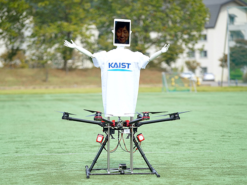 Robot Drone Man: A
Research Professor Ilhan Bae of the Moon Soul Graduate School of Future Strategy at KAIST created a life-size humanoid robot on a drone platform, which gives users the experience of virtual flight and an opportunity to interact with people at remote locations. Professor Bae calls his new creation a "telepresence robot."
This avatar drone is a new application of drone and robotics technology, which extends the reach of human presence and mobility, Professor Bae explained his research.
“As a futurist, I forecast that drone technology will soon evolve to become another body for humans, and I wanted to demonstrate this potential application of drones. Avatar drones are especially useful for people who need to meet or manage other people face to face in remote locations,” he said.
For example, if elderly people with physical disabilities want to engage in social gatherings, this avatar drone is designed to help them do just that.
For more details, please see the link below:
Behind the Music: How Robot Drone Man Built His Flying Avatar
IEEE Spectrum, November 7, 2016
2016.11.08 View 6717
Robot Drone Man: A
Research Professor Ilhan Bae of the Moon Soul Graduate School of Future Strategy at KAIST created a life-size humanoid robot on a drone platform, which gives users the experience of virtual flight and an opportunity to interact with people at remote locations. Professor Bae calls his new creation a "telepresence robot."
This avatar drone is a new application of drone and robotics technology, which extends the reach of human presence and mobility, Professor Bae explained his research.
“As a futurist, I forecast that drone technology will soon evolve to become another body for humans, and I wanted to demonstrate this potential application of drones. Avatar drones are especially useful for people who need to meet or manage other people face to face in remote locations,” he said.
For example, if elderly people with physical disabilities want to engage in social gatherings, this avatar drone is designed to help them do just that.
For more details, please see the link below:
Behind the Music: How Robot Drone Man Built His Flying Avatar
IEEE Spectrum, November 7, 2016
2016.11.08 View 6717 -
 Technology to Allow Non-Magnetic Materials to Have Magnetic Properties by Professor Chan-Ho Yang
Professor Chan-Ho Yang and his research team from the Department of Physics at KAIST have developed a technology that allows non-magnetic materials to have magnetic properties or, in reverse, to remove magnetic properties from a magnet using an electric field.
Based on this research, it is expected that if magnetic-material-based data storage is developed, applications for high-speed massive data transfer will be possible.
The results of this research, with Ph.D. candidate Byung-Kwon Jang as the first author, were published online in Nature Physics on October 3.
Very small magnets exist inside of any materials. If the direction of the minuscule magnets is dis-aligned, pointing multiple directions, it is non-magnetic. If the direction is aligned in a certain direction, the material holds magnetic property just like any magnet we normally see.
Data storage capacity technology has rapidly advanced to the point where we can easily get a portable hard disk drive (HDD) with terabyte-level storage; however, the increase in storage is inevitably followed by slower data access speed for a storage device. Although HDDs are currently the most widely used data storage devices, their technical applications are limited due to their slow data access speed.
Other methods such as solid-state drives (SSDs), floating gates, and resistive switching have been developed as alternatives. Yet, they leave tracks every time data is written, and this can cause fatigue cumulative damage.
There have been many attempts to compose cells—the smallest data storage space on a storage device—with magnetic materials as that would enable faster data access speeds and remove fatigue cumulative damage. Generally, the techniques tried by researchers were to use induced magnetic fields through current flow. However, magnetic fields are very difficult to shield and can affect a large area. As a result, they alternate the magnetic property of adjacent cells. Because each cell cannot be adjusted one by one, it cannot also be arranged in a certain direction, and therefore, it is hard to change the magnetic state.
Professor Yang and his team adjusted the magnetic state by using magnetoelectric interaction to deal with this issue. Instead of using magnetic fields, magnetoelectric interaction is a method that uses an electric field to adjust the magnetic state. It has the advantage of smaller energy consumption as well.
Professor Yang's team demonstrated that cells facing random directions can be arranged in a certain direction by only inducing an electric field. In addition, the reverse was also proved to be feasible.
Until this research, most cases of previous findings were only feasible at extremely low temperatures or high temperatures, but the technology developed by the research team is practicable at room temperature by manipulating chemical pressure. It allows for a reversible magnetic state, and moreover, is non-volatile. Therefore, the results of this research are expected to provide the basis for developing next-generation information storage device.
Professor Yang said, “The changes in the electric magnetic state will be accompanied by entropy changes” and added, “Our research is expected to open new potential for future applications not only for magnetoelectric devices, but also for thermoelectric effect.”
This research has been worked on jointly with Dr. Si-Yong Choi from the Korea Institute of Materials Science, Prof. Yoon-Hee Jeong from the Pohang University of Science and Technology, Dr. Tae-Yeong Koo from the Pohang Accelerator Laboratory, Dr. Kyung-Tae Ko from the Max Planck Institute for Chemical Physics of Solids, Dr. Jun-Sik Lee and Dr. Hendrik Ohldag from the SLAC National Accelerator Laboratory of the United States, and Prof. Jan Seidel from the University of New South Wales of Australia.
The research was supported by the Mid-Career Researcher Program of the National Research Foundation of Korea, Global Research Network Support Project, Leading Research Center Support Project (Condensed Quantum Coherence Research Center), Global Frontier Project (Hybrid Interface Materials Research Group), and others.
Picture: The concept graphic for the electric-field-induced magnetic phase switching the magnetic direction
2016.11.04 View 8774
Technology to Allow Non-Magnetic Materials to Have Magnetic Properties by Professor Chan-Ho Yang
Professor Chan-Ho Yang and his research team from the Department of Physics at KAIST have developed a technology that allows non-magnetic materials to have magnetic properties or, in reverse, to remove magnetic properties from a magnet using an electric field.
Based on this research, it is expected that if magnetic-material-based data storage is developed, applications for high-speed massive data transfer will be possible.
The results of this research, with Ph.D. candidate Byung-Kwon Jang as the first author, were published online in Nature Physics on October 3.
Very small magnets exist inside of any materials. If the direction of the minuscule magnets is dis-aligned, pointing multiple directions, it is non-magnetic. If the direction is aligned in a certain direction, the material holds magnetic property just like any magnet we normally see.
Data storage capacity technology has rapidly advanced to the point where we can easily get a portable hard disk drive (HDD) with terabyte-level storage; however, the increase in storage is inevitably followed by slower data access speed for a storage device. Although HDDs are currently the most widely used data storage devices, their technical applications are limited due to their slow data access speed.
Other methods such as solid-state drives (SSDs), floating gates, and resistive switching have been developed as alternatives. Yet, they leave tracks every time data is written, and this can cause fatigue cumulative damage.
There have been many attempts to compose cells—the smallest data storage space on a storage device—with magnetic materials as that would enable faster data access speeds and remove fatigue cumulative damage. Generally, the techniques tried by researchers were to use induced magnetic fields through current flow. However, magnetic fields are very difficult to shield and can affect a large area. As a result, they alternate the magnetic property of adjacent cells. Because each cell cannot be adjusted one by one, it cannot also be arranged in a certain direction, and therefore, it is hard to change the magnetic state.
Professor Yang and his team adjusted the magnetic state by using magnetoelectric interaction to deal with this issue. Instead of using magnetic fields, magnetoelectric interaction is a method that uses an electric field to adjust the magnetic state. It has the advantage of smaller energy consumption as well.
Professor Yang's team demonstrated that cells facing random directions can be arranged in a certain direction by only inducing an electric field. In addition, the reverse was also proved to be feasible.
Until this research, most cases of previous findings were only feasible at extremely low temperatures or high temperatures, but the technology developed by the research team is practicable at room temperature by manipulating chemical pressure. It allows for a reversible magnetic state, and moreover, is non-volatile. Therefore, the results of this research are expected to provide the basis for developing next-generation information storage device.
Professor Yang said, “The changes in the electric magnetic state will be accompanied by entropy changes” and added, “Our research is expected to open new potential for future applications not only for magnetoelectric devices, but also for thermoelectric effect.”
This research has been worked on jointly with Dr. Si-Yong Choi from the Korea Institute of Materials Science, Prof. Yoon-Hee Jeong from the Pohang University of Science and Technology, Dr. Tae-Yeong Koo from the Pohang Accelerator Laboratory, Dr. Kyung-Tae Ko from the Max Planck Institute for Chemical Physics of Solids, Dr. Jun-Sik Lee and Dr. Hendrik Ohldag from the SLAC National Accelerator Laboratory of the United States, and Prof. Jan Seidel from the University of New South Wales of Australia.
The research was supported by the Mid-Career Researcher Program of the National Research Foundation of Korea, Global Research Network Support Project, Leading Research Center Support Project (Condensed Quantum Coherence Research Center), Global Frontier Project (Hybrid Interface Materials Research Group), and others.
Picture: The concept graphic for the electric-field-induced magnetic phase switching the magnetic direction
2016.11.04 View 8774 -
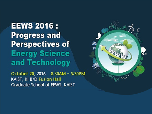 2016 KAIST EEWS Workshop
The Energy, Environment, Water and Sustainability (EEWS) Graduate School of KAIST hosted a workshop entitled “Progress and Perspectives of Energy Science and Technology” on October 20, 2016. The workshop took place at the Fusion Hall of the KAIST Institute on campus.
About 400 experts in energy science and engineering participated in the event. Eight globally recognized scientists introduced the latest research trends in nanomaterials, energy theory, catalysts, and photocatalysts and led discussions on the current status and prospects of EEWS.
Professors Yi Cui of Stanford University, an expert in nanomaterials, and William A. Goddard of California Institute of Technology presented their research experiments on materials design and recent results on the direction of theory under the topics of energy and environment.
Dr. Miquel Salmeron, a former head of the Material Science Division of Lawrence Berkeley National Laboratory, and Professor Yuichi Ikuhara of Tokyo University introduced their analysis of catalysts and energy matters at an atomic scale.
Professor Sukbok Chang of the Chemistry Department at KAIST, a deputy editor of ACS Catalysis and the head of the Center for Catalytic Hydrocarbon Functionalizations at the Institute of Basic Science, and Professor Yang-Kook Sun of Energy Engineering at Hanyang University, who is also a deputy editor of ACS Energy Letters, presented their latest research results on new catalytic reaction development and energy storage.
The workshop consisted of three sections which addressed the design of energy and environment materials; analysis of energy and catalytic materials; and energy conversion and catalysts.
The EEWS Graduate School was established in 2008 with the sponsorship of the Korean government’s World Class University (WCU) project to support science education in Korea. Professor J. Fraser Stoddart, the winner of the 2016 Nobel Prize in Chemistry, was previously worked at the KAIST EEWS Graduate School as a WCU visiting professor for two years, from 2011 to 2013. Professor Ali Coskun, who was a postdoctoral researcher in the laboratory of Professor Stoddart, now teaches and conducts research as a full-time professor at the graduate school.
Dean Yousung Jung of the EEWS Graduate School said:
“This workshop has provided us with a meaningful opportunity to engage in discussions on energy science and technology with world-class scholars from all around the world. It is also a good venue for our graduate school to share with them what we have been doing in research and education.”
2016.10.20 View 15049
2016 KAIST EEWS Workshop
The Energy, Environment, Water and Sustainability (EEWS) Graduate School of KAIST hosted a workshop entitled “Progress and Perspectives of Energy Science and Technology” on October 20, 2016. The workshop took place at the Fusion Hall of the KAIST Institute on campus.
About 400 experts in energy science and engineering participated in the event. Eight globally recognized scientists introduced the latest research trends in nanomaterials, energy theory, catalysts, and photocatalysts and led discussions on the current status and prospects of EEWS.
Professors Yi Cui of Stanford University, an expert in nanomaterials, and William A. Goddard of California Institute of Technology presented their research experiments on materials design and recent results on the direction of theory under the topics of energy and environment.
Dr. Miquel Salmeron, a former head of the Material Science Division of Lawrence Berkeley National Laboratory, and Professor Yuichi Ikuhara of Tokyo University introduced their analysis of catalysts and energy matters at an atomic scale.
Professor Sukbok Chang of the Chemistry Department at KAIST, a deputy editor of ACS Catalysis and the head of the Center for Catalytic Hydrocarbon Functionalizations at the Institute of Basic Science, and Professor Yang-Kook Sun of Energy Engineering at Hanyang University, who is also a deputy editor of ACS Energy Letters, presented their latest research results on new catalytic reaction development and energy storage.
The workshop consisted of three sections which addressed the design of energy and environment materials; analysis of energy and catalytic materials; and energy conversion and catalysts.
The EEWS Graduate School was established in 2008 with the sponsorship of the Korean government’s World Class University (WCU) project to support science education in Korea. Professor J. Fraser Stoddart, the winner of the 2016 Nobel Prize in Chemistry, was previously worked at the KAIST EEWS Graduate School as a WCU visiting professor for two years, from 2011 to 2013. Professor Ali Coskun, who was a postdoctoral researcher in the laboratory of Professor Stoddart, now teaches and conducts research as a full-time professor at the graduate school.
Dean Yousung Jung of the EEWS Graduate School said:
“This workshop has provided us with a meaningful opportunity to engage in discussions on energy science and technology with world-class scholars from all around the world. It is also a good venue for our graduate school to share with them what we have been doing in research and education.”
2016.10.20 View 15049 -
 KAIST Team Develops Semi-Transparent Solar Cells with Thermal Mirror Capability
A research team led by KAIST and Sungkyunkwan University professors has created semi-transparent perovskite solar cells that demonstrate high-power conversion efficiency and transmit visible light while blocking infrared light, making them great candidates for solar windows.
Modern architects prefer to build exteriors designed with glass mainly from artistic or cost perspectives. Scientists, however, go one step further and see opportunities from its potential ability to harness solar energy. Researchers have thus explored ways to make solar cells transparent or semi-transparent as a substitute material for glass, but this has proven to be a challenging task because solar cells need to absorb sunlight to generate electricity, and when they are transparent, it reduces their energy efficiency.
Typical solar cells today are made of crystalline silicon, but it is difficult to make them translucent. Semi-transparent solar cells under development use, for example, organic or dye-sensitized materials, but compared to crystalline silicon-based cells, their power-conversion efficiencies are relatively low. Perovskites are hybrid organic-inorganic halide-based photovoltaic materials, which are cheap to produce and easy to manufacture. They have recently received much attention as the efficiency of perovskite solar cells has rapidly increased to the level of silicon technologies in the past few years.
Using perovskites, a Korean research team led by Professor Seunghyup Yoo of the Electrical Engineering School at KAIST and Professor Nam-Gyu Park of the Chemical Engineering School at Sungkyunkwan University developed a semi-transparent solar cell that is highly efficient and, additionally, functions very effectively as a thermal-mirror.
The team has developed a top transparent electrode (TTE) that works well with perovskite solar cells. In most cases, a key to success in realizing semi-transparent solar cells is to find a TTE that is compatible with a given photoactive material system, which is also the case for perovskite solar cells. The proposed TTE is based on a multilayer stack consisting of a metal film sandwiched between a high refractive-index (high-index) layer and an interfacial buffer layer. This TTE, placed as a top-most layer, can be prepared without damaging ingredients used in perovskite solar cells. Unlike conventional transparent electrodes focusing only on transmitting visible light, the proposed TTE plays the dual role of passing through visible light while reflecting infrared rays. The semi-transparent solar cells made with the proposed TTEs exhibited average power conversion efficiency as high as 13.3% with 85.5% infrared rejection.
The team believes that if the semi-transparent perovskite solar cells are scaled up for practical applications, they can be used in solar windows for buildings and automobiles, which not only generate electrical energy but also enable the smart heat management for indoor environments, thereby utilizing solar energy more efficiently and effectively.
This result was published as a cover article in the July 20, 2016 issue of Advanced Energy Materials. The research paper is entitled “Empowering Semi-transparent Solar Cells with Thermal-mirror Functionality.” (DOI: 10.1002/aenm.201502466)
The team designed the transparent electrode (TE) stack in three layers: A thin-film of silver (Ag) is placed in between the bottom interfacial layer of molybdenum trioxide (MoO3) and the top high-index dielectric layer of zinc sulfide (ZnS). Such a tri-layer approach has been known as a means to increase the overall visible-light transmittance of metallic thin films via index matching technique, which is essentially the same technique used for anti-reflection coating of glasses except that the present case involves a metallic layer.
Traditionally, when a TE is based on a metal film, such as Ag, the film should be extremely thin, e.g., 7-12 nanometers (nm), to obtain transparency and, accordingly, to transmit visible light. However, the team took a different approach in this research. They made the Ag TE two or three times thicker (12-24 nm) than conventional metal films and, as a result, it reflected more infrared light. The high refractive index of the ZnS layer plays an essential role in keeping the visible light transmittance of the proposed TTE high even with the relatively thick Ag film when its thickness is carefully optimized for maximal destructive interference, leading to low reflectance (and thus high transmittance) within its visible light range.
The team confirmed the semi-transparent perovskite solar cell’s thermal-mirror function through an experiment in which a halogen lamp illuminated an object for five minutes through three mediums: a window of bare glass, automotive tinting film, and the proposed semi-transparent perovskite solar cell. An infrared (IR) camera took thermal images of the object as well as that of each window’s surface. The object’s temperature, when exposed through the glass window, rose to 36.8 Celsius degrees whereas both the tinting film and the cell allowed the object to remain below 27 Celsius degrees. The tinting film absorbs light to block solar energy, so the film’s surface became hot as it was continuously exposed to the lamp light, but the proposed semi-transparent solar cell stayed cool since it rejects solar heat energy by reflection, rather than by absorption. The total solar energy rejection (TSER) of the proposed cell was as high as 89.6%.
Professor Yoo of KAIST said, “The major contributions of this work are to find transparent electrode technology suitable for translucent perovskite cells and to provide a design approach to fully harness the potential it can further deliver as a heat mirror in addition to its main role as an electrode. The present work can be further fine-tuned to include colored solar cells and to incorporate flexible or rollable form factors, as they will allow for greater design freedom and thus offer more opportunities for them to be integrated into real-world objects and structures such as cars, buildings, and houses.”
The lead authors are Hoyeon Kim and Jaewon Ha, both Ph.D. candidates in the School of Electrical Engineering at KAIST, and Hui-Seon Kim, a student in the School of Chemical Engineering at Sungkyunkwan University. This research was supported mainly by the Climate Change Research Hub Program of KAIST.
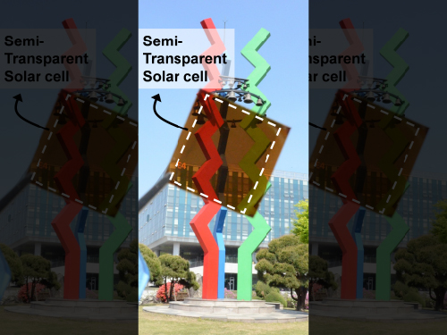
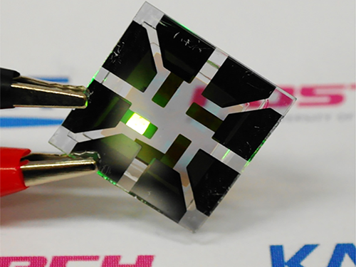
Picture 1: Semi-transparent Perovskite Solar Cell
This picture shows a prototype of a semi-transparent perovskite solar cell with thermal-mirror functionality.
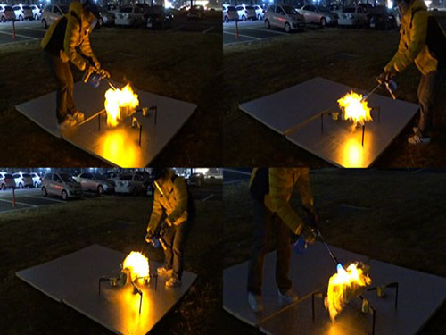
Picture 2: A Heat Rejection Performance Comparison Experiment
This picture presents thermal images taken by an infrared camera for comparing the heat rejection performance of bare glass, automotive tinting film, and a semi-transparent perovskite solar cell after being illuminated by a halogen lamp for five minutes.
2016.08.02 View 13820
KAIST Team Develops Semi-Transparent Solar Cells with Thermal Mirror Capability
A research team led by KAIST and Sungkyunkwan University professors has created semi-transparent perovskite solar cells that demonstrate high-power conversion efficiency and transmit visible light while blocking infrared light, making them great candidates for solar windows.
Modern architects prefer to build exteriors designed with glass mainly from artistic or cost perspectives. Scientists, however, go one step further and see opportunities from its potential ability to harness solar energy. Researchers have thus explored ways to make solar cells transparent or semi-transparent as a substitute material for glass, but this has proven to be a challenging task because solar cells need to absorb sunlight to generate electricity, and when they are transparent, it reduces their energy efficiency.
Typical solar cells today are made of crystalline silicon, but it is difficult to make them translucent. Semi-transparent solar cells under development use, for example, organic or dye-sensitized materials, but compared to crystalline silicon-based cells, their power-conversion efficiencies are relatively low. Perovskites are hybrid organic-inorganic halide-based photovoltaic materials, which are cheap to produce and easy to manufacture. They have recently received much attention as the efficiency of perovskite solar cells has rapidly increased to the level of silicon technologies in the past few years.
Using perovskites, a Korean research team led by Professor Seunghyup Yoo of the Electrical Engineering School at KAIST and Professor Nam-Gyu Park of the Chemical Engineering School at Sungkyunkwan University developed a semi-transparent solar cell that is highly efficient and, additionally, functions very effectively as a thermal-mirror.
The team has developed a top transparent electrode (TTE) that works well with perovskite solar cells. In most cases, a key to success in realizing semi-transparent solar cells is to find a TTE that is compatible with a given photoactive material system, which is also the case for perovskite solar cells. The proposed TTE is based on a multilayer stack consisting of a metal film sandwiched between a high refractive-index (high-index) layer and an interfacial buffer layer. This TTE, placed as a top-most layer, can be prepared without damaging ingredients used in perovskite solar cells. Unlike conventional transparent electrodes focusing only on transmitting visible light, the proposed TTE plays the dual role of passing through visible light while reflecting infrared rays. The semi-transparent solar cells made with the proposed TTEs exhibited average power conversion efficiency as high as 13.3% with 85.5% infrared rejection.
The team believes that if the semi-transparent perovskite solar cells are scaled up for practical applications, they can be used in solar windows for buildings and automobiles, which not only generate electrical energy but also enable the smart heat management for indoor environments, thereby utilizing solar energy more efficiently and effectively.
This result was published as a cover article in the July 20, 2016 issue of Advanced Energy Materials. The research paper is entitled “Empowering Semi-transparent Solar Cells with Thermal-mirror Functionality.” (DOI: 10.1002/aenm.201502466)
The team designed the transparent electrode (TE) stack in three layers: A thin-film of silver (Ag) is placed in between the bottom interfacial layer of molybdenum trioxide (MoO3) and the top high-index dielectric layer of zinc sulfide (ZnS). Such a tri-layer approach has been known as a means to increase the overall visible-light transmittance of metallic thin films via index matching technique, which is essentially the same technique used for anti-reflection coating of glasses except that the present case involves a metallic layer.
Traditionally, when a TE is based on a metal film, such as Ag, the film should be extremely thin, e.g., 7-12 nanometers (nm), to obtain transparency and, accordingly, to transmit visible light. However, the team took a different approach in this research. They made the Ag TE two or three times thicker (12-24 nm) than conventional metal films and, as a result, it reflected more infrared light. The high refractive index of the ZnS layer plays an essential role in keeping the visible light transmittance of the proposed TTE high even with the relatively thick Ag film when its thickness is carefully optimized for maximal destructive interference, leading to low reflectance (and thus high transmittance) within its visible light range.
The team confirmed the semi-transparent perovskite solar cell’s thermal-mirror function through an experiment in which a halogen lamp illuminated an object for five minutes through three mediums: a window of bare glass, automotive tinting film, and the proposed semi-transparent perovskite solar cell. An infrared (IR) camera took thermal images of the object as well as that of each window’s surface. The object’s temperature, when exposed through the glass window, rose to 36.8 Celsius degrees whereas both the tinting film and the cell allowed the object to remain below 27 Celsius degrees. The tinting film absorbs light to block solar energy, so the film’s surface became hot as it was continuously exposed to the lamp light, but the proposed semi-transparent solar cell stayed cool since it rejects solar heat energy by reflection, rather than by absorption. The total solar energy rejection (TSER) of the proposed cell was as high as 89.6%.
Professor Yoo of KAIST said, “The major contributions of this work are to find transparent electrode technology suitable for translucent perovskite cells and to provide a design approach to fully harness the potential it can further deliver as a heat mirror in addition to its main role as an electrode. The present work can be further fine-tuned to include colored solar cells and to incorporate flexible or rollable form factors, as they will allow for greater design freedom and thus offer more opportunities for them to be integrated into real-world objects and structures such as cars, buildings, and houses.”
The lead authors are Hoyeon Kim and Jaewon Ha, both Ph.D. candidates in the School of Electrical Engineering at KAIST, and Hui-Seon Kim, a student in the School of Chemical Engineering at Sungkyunkwan University. This research was supported mainly by the Climate Change Research Hub Program of KAIST.
Picture 1: Semi-transparent Perovskite Solar Cell
This picture shows a prototype of a semi-transparent perovskite solar cell with thermal-mirror functionality.
Picture 2: A Heat Rejection Performance Comparison Experiment
This picture presents thermal images taken by an infrared camera for comparing the heat rejection performance of bare glass, automotive tinting film, and a semi-transparent perovskite solar cell after being illuminated by a halogen lamp for five minutes.
2016.08.02 View 13820 -
 Graphene-Based Transparent Electrodes for Highly Efficient Flexible OLEDs
A Korean research team developed an ideal electrode structure composed of graphene and layers of titanium dioxide and conducting polymers, resulting in highly flexible and efficient OLEDs.
The arrival of a thin and lightweight computer that even rolls up like a piece of paper will not be in the far distant future. Flexible organic light-emitting diodes (OLEDs), built upon a plastic substrate, have received greater attention lately for their use in next-generation displays that can be bent or rolled while still operating.
A Korean research team led by Professor Seunghyup Yoo from the School of Electrical Engineering, KAIST and Professor Tae-Woo Lee from the Department of Materials Science and Engineering, Pohang University of Science and Technology (POSTECH) has developed highly flexible OLEDs with excellent efficiency by using graphene as a transparent electrode (TE) which is placed in between titanium dioxide (TiO2) and conducting polymer layers. The research results were published online on June 2, 2016 in Nature Communications.
OLEDs are stacked in several ultra-thin layers on glass, foil, or plastic substrates, in which multi-layers of organic compounds are sandwiched between two electrodes (cathode and anode). When voltage is applied across the electrodes, electrons from the cathode and holes (positive charges) from the anode draw toward each other and meet in the emissive layer. OLEDs emit light as an electron recombines with a positive hole, releasing energy in the form of a photon. One of the electrodes in OLEDs is usually transparent, and depending on which electrode is transparent, OLEDs can either emit from the top or bottom.
In conventional bottom-emission OLEDs, an anode is transparent in order for the emitted photons to exit the device through its substrate. Indium-tin-oxide (ITO) is commonly used as a transparent anode because of its high transparency, low sheet resistance, and well-established manufacturing process. However, ITO can potentially be expensive, and moreover, is brittle, being susceptible to bending-induced formation of cracks.
Graphene, a two-dimensional thin layer of carbon atoms tightly bonded together in a hexagonal honeycomb lattice, has recently emerged as an alternative to ITO. With outstanding electrical, physical, and chemical properties, its atomic thinness leading to a high degree of flexibility and transparency makes it an ideal candidate for TEs. Nonetheless, the efficiency of graphene-based OLEDs reported to date has been, at best, about the same level of ITO-based OLEDs.
As a solution, the Korean research team, which further includes Professors Sung-Yool Choi (Electrical Engineering) and Taek-Soo Kim (Mechanical Engineering) of KAIST and their students, proposed a new device architecture that can maximize the efficiency of graphene-based OLEDs. They fabricated a transparent anode in a composite structure in which a TiO2 layer with a high refractive index (high-n) and a hole-injection layer (HIL) of conducting polymers with a low refractive index (low-n) sandwich graphene electrodes. This is an optical design that induces a synergistic collaboration between the high-n and low-n layers to increase the effective reflectance of TEs. As a result, the enhancement of the optical cavity resonance is maximized. The optical cavity resonance is related to the improvement of efficiency and color gamut in OLEDs. At the same time, the loss from surface plasmon polariton (SPP), a major cause for weak photon emissions in OLEDs, is also reduced due to the presence of the low-n conducting polymers.
Under this approach, graphene-based OLEDs exhibit 40.8% of ultrahigh external quantum efficiency (EQE) and 160.3 lm/W of power efficiency, which is unprecedented in those using graphene as a TE. Furthermore, these devices remain intact and operate well even after 1,000 bending cycles at a radius of curvature as small as 2.3 mm. This is a remarkable result for OLEDs containing oxide layers such as TiO2 because oxides are typically brittle and prone to bending-induced fractures even at a relatively low strain. The research team discovered that TiO2 has a crack-deflection toughening mechanism that tends to prevent bending-induced cracks from being formed easily.
Professor Yoo said, “What’s unique and advanced about this technology, compared with previous graphene-based OLEDs, is the synergistic collaboration of high- and low-index layers that enables optical management of both resonance effect and SPP loss, leading to significant enhancement in efficiency, all with little compromise in flexibility.” He added, “Our work was the achievement of collaborative research, transcending the boundaries of different fields, through which we have often found meaningful breakthroughs.”
Professor Lee said, “We expect that our technology will pave the way to develop an OLED light source for highly flexible and wearable displays, or flexible sensors that can be attached to the human body for health monitoring, for instance.”
The research paper is entitled “Synergistic Electrode Architecture for Efficient Graphene-based Flexible Organic Light-emitting Diodes” (DOI. 10.1038/NCOMMS11791). The lead authors are Jae-Ho Lee, a Ph.D. candidate at KAIST; Tae-Hee Han, a Ph.D. researcher at POSTECH; and Min-Ho Park, a Ph.D. candidate at POSTECH.
This study was supported by the Basic Science Research Program of the National Research Foundation of Korea (NRF) through the Center for Advanced Flexible Display (CAFDC) funded by the Ministry of Science, ICT and Future Planning (MSIP); by the Center for Advanced Soft-Electronics funded by the MSIP as a Global Frontier Project; by the Graphene Research Center Program of KAIST; and by grants from the IT R&D Program of the Ministry of Trade, Industry and Energy of Korea (MOTIE).
Figure 1: Application of Graphene-based OLEDs
This picture shows an OLED with the composite structure of TiO2/graphene/conducting polymer electrode in operation. The OLED exhibits 40.8% of ultrahigh external quantum efficiency (EQE) and 160.3 lm/W of power efficiency. The device prepared on a plastic substrate shown in the right remains intact and operates well even after 1,000 bending cycles at a radius of curvature as small as 2.3 mm.
Figure 2: Schematic Device Structure of Graphene-based OLEDs
This picture shows the new architecture to develop highly flexible OLEDs with excellent efficiency by using graphene as a transparent electrode (TE).
2016.06.07 View 15792
Graphene-Based Transparent Electrodes for Highly Efficient Flexible OLEDs
A Korean research team developed an ideal electrode structure composed of graphene and layers of titanium dioxide and conducting polymers, resulting in highly flexible and efficient OLEDs.
The arrival of a thin and lightweight computer that even rolls up like a piece of paper will not be in the far distant future. Flexible organic light-emitting diodes (OLEDs), built upon a plastic substrate, have received greater attention lately for their use in next-generation displays that can be bent or rolled while still operating.
A Korean research team led by Professor Seunghyup Yoo from the School of Electrical Engineering, KAIST and Professor Tae-Woo Lee from the Department of Materials Science and Engineering, Pohang University of Science and Technology (POSTECH) has developed highly flexible OLEDs with excellent efficiency by using graphene as a transparent electrode (TE) which is placed in between titanium dioxide (TiO2) and conducting polymer layers. The research results were published online on June 2, 2016 in Nature Communications.
OLEDs are stacked in several ultra-thin layers on glass, foil, or plastic substrates, in which multi-layers of organic compounds are sandwiched between two electrodes (cathode and anode). When voltage is applied across the electrodes, electrons from the cathode and holes (positive charges) from the anode draw toward each other and meet in the emissive layer. OLEDs emit light as an electron recombines with a positive hole, releasing energy in the form of a photon. One of the electrodes in OLEDs is usually transparent, and depending on which electrode is transparent, OLEDs can either emit from the top or bottom.
In conventional bottom-emission OLEDs, an anode is transparent in order for the emitted photons to exit the device through its substrate. Indium-tin-oxide (ITO) is commonly used as a transparent anode because of its high transparency, low sheet resistance, and well-established manufacturing process. However, ITO can potentially be expensive, and moreover, is brittle, being susceptible to bending-induced formation of cracks.
Graphene, a two-dimensional thin layer of carbon atoms tightly bonded together in a hexagonal honeycomb lattice, has recently emerged as an alternative to ITO. With outstanding electrical, physical, and chemical properties, its atomic thinness leading to a high degree of flexibility and transparency makes it an ideal candidate for TEs. Nonetheless, the efficiency of graphene-based OLEDs reported to date has been, at best, about the same level of ITO-based OLEDs.
As a solution, the Korean research team, which further includes Professors Sung-Yool Choi (Electrical Engineering) and Taek-Soo Kim (Mechanical Engineering) of KAIST and their students, proposed a new device architecture that can maximize the efficiency of graphene-based OLEDs. They fabricated a transparent anode in a composite structure in which a TiO2 layer with a high refractive index (high-n) and a hole-injection layer (HIL) of conducting polymers with a low refractive index (low-n) sandwich graphene electrodes. This is an optical design that induces a synergistic collaboration between the high-n and low-n layers to increase the effective reflectance of TEs. As a result, the enhancement of the optical cavity resonance is maximized. The optical cavity resonance is related to the improvement of efficiency and color gamut in OLEDs. At the same time, the loss from surface plasmon polariton (SPP), a major cause for weak photon emissions in OLEDs, is also reduced due to the presence of the low-n conducting polymers.
Under this approach, graphene-based OLEDs exhibit 40.8% of ultrahigh external quantum efficiency (EQE) and 160.3 lm/W of power efficiency, which is unprecedented in those using graphene as a TE. Furthermore, these devices remain intact and operate well even after 1,000 bending cycles at a radius of curvature as small as 2.3 mm. This is a remarkable result for OLEDs containing oxide layers such as TiO2 because oxides are typically brittle and prone to bending-induced fractures even at a relatively low strain. The research team discovered that TiO2 has a crack-deflection toughening mechanism that tends to prevent bending-induced cracks from being formed easily.
Professor Yoo said, “What’s unique and advanced about this technology, compared with previous graphene-based OLEDs, is the synergistic collaboration of high- and low-index layers that enables optical management of both resonance effect and SPP loss, leading to significant enhancement in efficiency, all with little compromise in flexibility.” He added, “Our work was the achievement of collaborative research, transcending the boundaries of different fields, through which we have often found meaningful breakthroughs.”
Professor Lee said, “We expect that our technology will pave the way to develop an OLED light source for highly flexible and wearable displays, or flexible sensors that can be attached to the human body for health monitoring, for instance.”
The research paper is entitled “Synergistic Electrode Architecture for Efficient Graphene-based Flexible Organic Light-emitting Diodes” (DOI. 10.1038/NCOMMS11791). The lead authors are Jae-Ho Lee, a Ph.D. candidate at KAIST; Tae-Hee Han, a Ph.D. researcher at POSTECH; and Min-Ho Park, a Ph.D. candidate at POSTECH.
This study was supported by the Basic Science Research Program of the National Research Foundation of Korea (NRF) through the Center for Advanced Flexible Display (CAFDC) funded by the Ministry of Science, ICT and Future Planning (MSIP); by the Center for Advanced Soft-Electronics funded by the MSIP as a Global Frontier Project; by the Graphene Research Center Program of KAIST; and by grants from the IT R&D Program of the Ministry of Trade, Industry and Energy of Korea (MOTIE).
Figure 1: Application of Graphene-based OLEDs
This picture shows an OLED with the composite structure of TiO2/graphene/conducting polymer electrode in operation. The OLED exhibits 40.8% of ultrahigh external quantum efficiency (EQE) and 160.3 lm/W of power efficiency. The device prepared on a plastic substrate shown in the right remains intact and operates well even after 1,000 bending cycles at a radius of curvature as small as 2.3 mm.
Figure 2: Schematic Device Structure of Graphene-based OLEDs
This picture shows the new architecture to develop highly flexible OLEDs with excellent efficiency by using graphene as a transparent electrode (TE).
2016.06.07 View 15792 -
 A Firefighter Drone That Flies and Crawls Up Walls
KAIST researchers developed a wall-climbing scout drone to fight fires in high-rises, finding the source of the fires and locating people trapped inside.
The 1974 American disaster film Towering Inferno depicted well the earnest struggles of firefighters engaged in ending a fire at a 138-story skyscraper. To this day, fires at high-rise buildings are considered one of the most dangerous disasters.
Skyscraper fires are particularly difficult to contain because of their ability to spread rapidly in high-occupant density spaces and the challenge of fighting fires in the buildings’ complex vertical structure. Accessibility to skyscrapers at the time of the fire is limited, and it is hard to assess the initial situation.
A research team at KAIST led by Professor Hyun Myung of the Civil and Environmental Engineering Department developed an unmanned aerial vehicle, named the Fireproof Aerial RObot System (FAROS), which detects fires in skyscrapers, searches the inside of the building, and transfers data in real time from fire scenes to the ground station.
As an extended version of Climbing Aerial RObot System (CAROS) that was created in 2014 by the research team, the FAROS can also fly and climb walls.
The FAROS, whose movements rely on a quadrotor system, can freely change its flight mode into a spider’s crawling on walls, and vice versa, facilitating unimpeded navigation in the labyrinth of narrow spaces filled with debris and rubble inside the blazing building.
The drone “estimates” its pose by utilizing a 2-D laser scanner, an altimeter, and an Inertia Measurement Unit sensor to navigate autonomously. With the localization result and using a thermal-imaging camera to recognize objects or people inside a building, the FAROS can also detect and find the fire-ignition point by employing dedicated image-processing technology.
The FAROS is fireproof and flame-retardant. The drone’s body is covered with aramid fibers to protect its electric and mechanical components from the direct effects of the flame. The aramid fiber skin also has a buffer of air underneath it, and a thermoelectric cooling system based on the Peltier effect to help maintain the air layer within a specific temperature range.
The research team demonstrated the feasibility of the localization system and wall-climbing mechanism in a smoky indoor environment. The fireproof test showed that the drone could endure the heat of over 1,000° Celsius from butane gas and ethanol aerosol flames for over one minute.
Professor Myung said, “As cities become more crowded with skyscrapers and super structures, fire incidents in these high-rise buildings are life-threatening massive disasters. The FAROS can be aptly deployed to the disaster site at an early stage of such incidents to minimize the damage and maximize the safety and efficiency of rescue mission.”
The research team has recently started to enhance the performance of the fireproof design for the exteroceptive sensors including a 2-D laser scanner and a thermal-imaging camera because those sensors could be more exposed to fire than other inside sensors and electric components.
This research was funded by the KAIST Initiative for Disaster Studies and the KAIST Institute.
YouTube link: https://youtu.be/gPNRZi0EPQw
Picture 1: Demonstration of Wall-climbing
The Fireproof Aerial RObot System (FAROS) is a wall-climbing scout drone developed to conduct explorations into the site of skyscraper fires. It has an ability to climb walls in smoky, narrow spaces inside buildings.
Figure 2: An Ability to Withstand Fires
The FAROS can endure the heat of over 1,000° Celsius from butane gas and ethanol aerosol flames for over one minute.
2016.01.20 View 16495
A Firefighter Drone That Flies and Crawls Up Walls
KAIST researchers developed a wall-climbing scout drone to fight fires in high-rises, finding the source of the fires and locating people trapped inside.
The 1974 American disaster film Towering Inferno depicted well the earnest struggles of firefighters engaged in ending a fire at a 138-story skyscraper. To this day, fires at high-rise buildings are considered one of the most dangerous disasters.
Skyscraper fires are particularly difficult to contain because of their ability to spread rapidly in high-occupant density spaces and the challenge of fighting fires in the buildings’ complex vertical structure. Accessibility to skyscrapers at the time of the fire is limited, and it is hard to assess the initial situation.
A research team at KAIST led by Professor Hyun Myung of the Civil and Environmental Engineering Department developed an unmanned aerial vehicle, named the Fireproof Aerial RObot System (FAROS), which detects fires in skyscrapers, searches the inside of the building, and transfers data in real time from fire scenes to the ground station.
As an extended version of Climbing Aerial RObot System (CAROS) that was created in 2014 by the research team, the FAROS can also fly and climb walls.
The FAROS, whose movements rely on a quadrotor system, can freely change its flight mode into a spider’s crawling on walls, and vice versa, facilitating unimpeded navigation in the labyrinth of narrow spaces filled with debris and rubble inside the blazing building.
The drone “estimates” its pose by utilizing a 2-D laser scanner, an altimeter, and an Inertia Measurement Unit sensor to navigate autonomously. With the localization result and using a thermal-imaging camera to recognize objects or people inside a building, the FAROS can also detect and find the fire-ignition point by employing dedicated image-processing technology.
The FAROS is fireproof and flame-retardant. The drone’s body is covered with aramid fibers to protect its electric and mechanical components from the direct effects of the flame. The aramid fiber skin also has a buffer of air underneath it, and a thermoelectric cooling system based on the Peltier effect to help maintain the air layer within a specific temperature range.
The research team demonstrated the feasibility of the localization system and wall-climbing mechanism in a smoky indoor environment. The fireproof test showed that the drone could endure the heat of over 1,000° Celsius from butane gas and ethanol aerosol flames for over one minute.
Professor Myung said, “As cities become more crowded with skyscrapers and super structures, fire incidents in these high-rise buildings are life-threatening massive disasters. The FAROS can be aptly deployed to the disaster site at an early stage of such incidents to minimize the damage and maximize the safety and efficiency of rescue mission.”
The research team has recently started to enhance the performance of the fireproof design for the exteroceptive sensors including a 2-D laser scanner and a thermal-imaging camera because those sensors could be more exposed to fire than other inside sensors and electric components.
This research was funded by the KAIST Initiative for Disaster Studies and the KAIST Institute.
YouTube link: https://youtu.be/gPNRZi0EPQw
Picture 1: Demonstration of Wall-climbing
The Fireproof Aerial RObot System (FAROS) is a wall-climbing scout drone developed to conduct explorations into the site of skyscraper fires. It has an ability to climb walls in smoky, narrow spaces inside buildings.
Figure 2: An Ability to Withstand Fires
The FAROS can endure the heat of over 1,000° Celsius from butane gas and ethanol aerosol flames for over one minute.
2016.01.20 View 16495 -
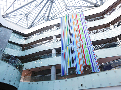 KAIST Holds Its Fourth Public Art Exhibition
KAIST hosted an opening ceremony for the annual art exhibition on December 3, 2015 at the KAIST Institute building. The KAIST Art and Design Committee first organized the event in 2012 to promote the integration of art and technology.
This year’s event entitled “Understanding the Purpose of an Object” will display 20 art pieces under six themes. Artist Keumhong Lee, Haeyool Roh, Joon Kim, Kyung Lee, and Juhae Yang participated in the exhibition. The names of some of the art pieces include “Feedback Field” by Joon Kim, “Self Action” by Haeyool Roh, and “Net of Time” by Juhae Yang.
Juhae Yang believes that, in the digital age, an identity of an object is defined by the traces of light which we read in the information hidden in the barcodes. Based on this interpretation, she transforms the black bars and white spaces into a harmony of colors and sounds. The continuum of colors and sounds in her work arouses time-space synesthesia.
Professor Sangmin Bae of the Industrial Design Department, the Director of the KAIST Art and Design Committee, hopes that the exhibition will inspire novel scientific ideas and artistic spirits.
The exhibition will remain open to the public until December 20, 2015.
2015.12.03 View 10617
KAIST Holds Its Fourth Public Art Exhibition
KAIST hosted an opening ceremony for the annual art exhibition on December 3, 2015 at the KAIST Institute building. The KAIST Art and Design Committee first organized the event in 2012 to promote the integration of art and technology.
This year’s event entitled “Understanding the Purpose of an Object” will display 20 art pieces under six themes. Artist Keumhong Lee, Haeyool Roh, Joon Kim, Kyung Lee, and Juhae Yang participated in the exhibition. The names of some of the art pieces include “Feedback Field” by Joon Kim, “Self Action” by Haeyool Roh, and “Net of Time” by Juhae Yang.
Juhae Yang believes that, in the digital age, an identity of an object is defined by the traces of light which we read in the information hidden in the barcodes. Based on this interpretation, she transforms the black bars and white spaces into a harmony of colors and sounds. The continuum of colors and sounds in her work arouses time-space synesthesia.
Professor Sangmin Bae of the Industrial Design Department, the Director of the KAIST Art and Design Committee, hopes that the exhibition will inspire novel scientific ideas and artistic spirits.
The exhibition will remain open to the public until December 20, 2015.
2015.12.03 View 10617 -
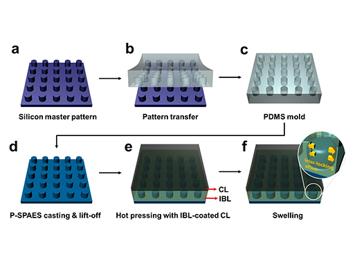 Membrane
Scientists at KAIST have developed a new way of making fuel cell membranes using nanoscale fasteners, paving the way for lower-cost, higher-efficiency and more easily manufactured fuel cells.
The internal workings of fuel cells vary, but basically all types mix hydrogen and oxygen to produce a chemical reaction that delivers usable electricity and exhausts ordinary water as a by-product. One of the most efficient types is the proton exchange membrane (PEM) fuel cell, which operates at low enough temperatures to be used in homes and vehicles.
To generate electricity, PEM fuel cells rely on two chemical compartments separated by a permeable catalyst membrane. This membrane acts as an electrolyte; a negative electrode is bonded to one side of the membrane and a positive electrode is bonded to the other. The electrolyte membrane is often based on a polymer of perfluorosulfonic acid. Due to its high cost, however, a less expensive hydrocarbon-based electrolyte membrane has attracted interest in this technology sector.
Until now, the challenge in adopting such a hydrocarbon membrane has been that the interface between the electrode and hydrocarbon membrane is weak. This causes the membrane to delaminate relatively easily, falling apart and losing efficiency with use.
Professor Hee-Tak Kim of the Department of Chemical and Biomolecular Engineering at the Korea Advanced Institute of Science and Technology (KAIST) and his research team have developed a new fastening system that bonds the two materials mechanically rather than chemically. This opens the way to the development of fuel cell membranes that are less expensive, easier to manufacture, stronger and more efficient.
The researchers achieved this by moulding a pattern of tiny cylindrical pillars on the face of the hydrocarbon membrane. The pillars protrude into a softened skin of the electrode with heat. The mechanical bond sets and strengthens as the material cools and absorbs water. The pillar-patterned hydrocarbon membrane is cast using silicone moulds.
Professor Kim said, “This physically fastened bond is almost five times stronger and harder to separate than current bonds between the same layers.”
The new interlocking method also appears to offer a way to bond many types of hydrocarbon membranes that, until now, have been rejected because they couldn’t be fastened robustly. This would make hydrocarbon membranes practical for a number of applications beyond fuel cells such as rechargeable “redox flow” batteries.
The research team is now developing a stronger and more scalable interlocking interface for their nanoscale fasteners.
Picture: Schematic Diagram of the Fabrication of the Pillar P-SPAES Membrane and Its Working Principle of Interlocking Effects
2015.11.06 View 10802
Membrane
Scientists at KAIST have developed a new way of making fuel cell membranes using nanoscale fasteners, paving the way for lower-cost, higher-efficiency and more easily manufactured fuel cells.
The internal workings of fuel cells vary, but basically all types mix hydrogen and oxygen to produce a chemical reaction that delivers usable electricity and exhausts ordinary water as a by-product. One of the most efficient types is the proton exchange membrane (PEM) fuel cell, which operates at low enough temperatures to be used in homes and vehicles.
To generate electricity, PEM fuel cells rely on two chemical compartments separated by a permeable catalyst membrane. This membrane acts as an electrolyte; a negative electrode is bonded to one side of the membrane and a positive electrode is bonded to the other. The electrolyte membrane is often based on a polymer of perfluorosulfonic acid. Due to its high cost, however, a less expensive hydrocarbon-based electrolyte membrane has attracted interest in this technology sector.
Until now, the challenge in adopting such a hydrocarbon membrane has been that the interface between the electrode and hydrocarbon membrane is weak. This causes the membrane to delaminate relatively easily, falling apart and losing efficiency with use.
Professor Hee-Tak Kim of the Department of Chemical and Biomolecular Engineering at the Korea Advanced Institute of Science and Technology (KAIST) and his research team have developed a new fastening system that bonds the two materials mechanically rather than chemically. This opens the way to the development of fuel cell membranes that are less expensive, easier to manufacture, stronger and more efficient.
The researchers achieved this by moulding a pattern of tiny cylindrical pillars on the face of the hydrocarbon membrane. The pillars protrude into a softened skin of the electrode with heat. The mechanical bond sets and strengthens as the material cools and absorbs water. The pillar-patterned hydrocarbon membrane is cast using silicone moulds.
Professor Kim said, “This physically fastened bond is almost five times stronger and harder to separate than current bonds between the same layers.”
The new interlocking method also appears to offer a way to bond many types of hydrocarbon membranes that, until now, have been rejected because they couldn’t be fastened robustly. This would make hydrocarbon membranes practical for a number of applications beyond fuel cells such as rechargeable “redox flow” batteries.
The research team is now developing a stronger and more scalable interlocking interface for their nanoscale fasteners.
Picture: Schematic Diagram of the Fabrication of the Pillar P-SPAES Membrane and Its Working Principle of Interlocking Effects
2015.11.06 View 10802 -
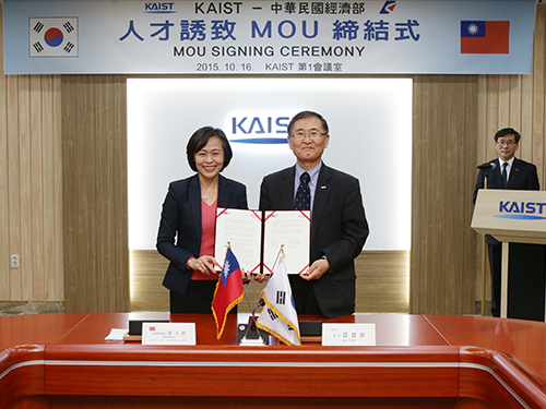 KAIST Agrees to Personnel Exchange with the Ministry of Economic Affairs of the Republic of China
A delegation from the Ministry of Economic Affairs (MOEA) of the Republic of China (ROC) visited KAIST on October 16, 2015.
President Steve Kang of KAIST and Director General Yu-Ping Lien of the Department of Investment Services, MOEA, signed a memorandum of understanding (MOU) on exchanging personnel, recruiting and attracting top talents, and sharing job information.
With the MOU, KAIST and MOEA will develop a mobility program for students in Korea and ROC to help them seek employment opportunities in both nations. Director General Lien hoped that the MOU would bring more of KAIST students in the information technology field to work in ROC.
President Kang responded,
“KAIST has fostered highly talented engineers and researchers across all fields of science and engineering. If these students can have a place in ROC to realize their potential, this certainly could benefit the two nations.”
In the picture from left to right is Director General Yu-Ping Lien of the Department of Investment Services, the Ministry of Economic Affairs of the Republic of China and President Steve Kang of KAIST.
2015.10.17 View 6367
KAIST Agrees to Personnel Exchange with the Ministry of Economic Affairs of the Republic of China
A delegation from the Ministry of Economic Affairs (MOEA) of the Republic of China (ROC) visited KAIST on October 16, 2015.
President Steve Kang of KAIST and Director General Yu-Ping Lien of the Department of Investment Services, MOEA, signed a memorandum of understanding (MOU) on exchanging personnel, recruiting and attracting top talents, and sharing job information.
With the MOU, KAIST and MOEA will develop a mobility program for students in Korea and ROC to help them seek employment opportunities in both nations. Director General Lien hoped that the MOU would bring more of KAIST students in the information technology field to work in ROC.
President Kang responded,
“KAIST has fostered highly talented engineers and researchers across all fields of science and engineering. If these students can have a place in ROC to realize their potential, this certainly could benefit the two nations.”
In the picture from left to right is Director General Yu-Ping Lien of the Department of Investment Services, the Ministry of Economic Affairs of the Republic of China and President Steve Kang of KAIST.
2015.10.17 View 6367 -
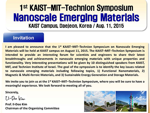 KAIST holds the 2015 KAIST-MIT-Technion International Symposium on Nano Science
The 2015 KAIST-MIT-Technion International Symposium on Nano Science was held on August 11, 2015 at the KAIST campus. The event took place under three subtopics: Materials for Production and Storage of Renewable Energy, Functional Materials, and Multiferroic Materials.
The joint symposium invited more than 300 experts in material science and engineering including ten speakers and panelists. From MIT (Massachusetts Institute of Technology), Professors Harry L. Tuller and Geoffrey S. Beach in the Department of Material Engineering, as well as Professor Gregory Rutledge in the Department of Chemical Engineering joined the symposium. Professor Avner Rothschild in the Department of Material Engineering and Professor Yair Ein-Eli in the Department of Chemical Engineering at Technion Institute of Technology in Israel also participated.
From KAIST, Professors Il-Doo Kim, Byong-Guk Park, and Yeon-Sik Jung in the Department of Materials Science and Engineering, Professor Chan-Ho Yang in the Department of Physics, and Professor Doh-Chang Lee in the Department of Chemical and Biomolecular Engineering spoke at the event. The list of topics included “Next Generation Lithium-Air Battery,” “Nano Materials for High Performance Energy Storage System,” and “Iron Oxide Nanoparticles Photoelectrode for the Conversion and Storage of Solar Energy.”
In its efforts to promote cooperation among the three universities, KAIST plans to send six students to MIT and one student to Technion for joint research.
Professor Il-Doo Kim, who organized the symposium said, “We believe this kind of international gathering will serve as an opportunity for scholars from leading universities to share their expertise in material science and help them better understand on the recent trends in nanoscience and its related technology.”
2015.08.12 View 10105
KAIST holds the 2015 KAIST-MIT-Technion International Symposium on Nano Science
The 2015 KAIST-MIT-Technion International Symposium on Nano Science was held on August 11, 2015 at the KAIST campus. The event took place under three subtopics: Materials for Production and Storage of Renewable Energy, Functional Materials, and Multiferroic Materials.
The joint symposium invited more than 300 experts in material science and engineering including ten speakers and panelists. From MIT (Massachusetts Institute of Technology), Professors Harry L. Tuller and Geoffrey S. Beach in the Department of Material Engineering, as well as Professor Gregory Rutledge in the Department of Chemical Engineering joined the symposium. Professor Avner Rothschild in the Department of Material Engineering and Professor Yair Ein-Eli in the Department of Chemical Engineering at Technion Institute of Technology in Israel also participated.
From KAIST, Professors Il-Doo Kim, Byong-Guk Park, and Yeon-Sik Jung in the Department of Materials Science and Engineering, Professor Chan-Ho Yang in the Department of Physics, and Professor Doh-Chang Lee in the Department of Chemical and Biomolecular Engineering spoke at the event. The list of topics included “Next Generation Lithium-Air Battery,” “Nano Materials for High Performance Energy Storage System,” and “Iron Oxide Nanoparticles Photoelectrode for the Conversion and Storage of Solar Energy.”
In its efforts to promote cooperation among the three universities, KAIST plans to send six students to MIT and one student to Technion for joint research.
Professor Il-Doo Kim, who organized the symposium said, “We believe this kind of international gathering will serve as an opportunity for scholars from leading universities to share their expertise in material science and help them better understand on the recent trends in nanoscience and its related technology.”
2015.08.12 View 10105