Electrical+Engineering
-
 Lens-free OLEDs with Efficiency comparable to that of Inorganic LEDs
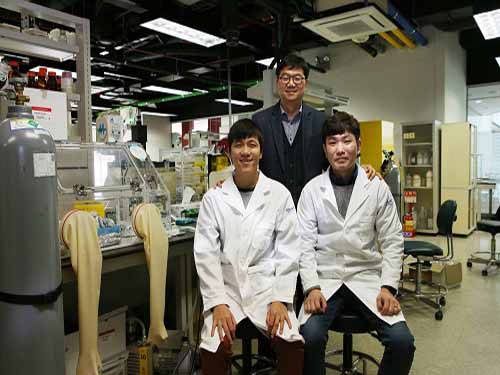
(from left: Professor Seunghyup Yoo and PhD candidate Jinouk Song)
The use of organic light-emitting diodes (OLEDs) has extended to various applications, but their efficiency is still lagging behind inorganic light-emitting diodes. In this research, a KAIST team provided a systematic way to yield OLEDs with an external quantum efficiency (EQE) greater than 50% with an external scattering medium.
Having properties suitable for thin and flexible devices, OLEDs are popular light sources for displays, such as mobile devices and high quality TVs. In recent years, numerous efforts have been made to apply OLEDs in lighting as well as light sources for vehicles.
For such applications, high efficiency is of the upmost importance for the successful deployment of light sources. Thanks to continuous research and the development of OLEDs, their efficiency is steadily on the rise, and a level equivalent to inorganic LEDs has been demonstrated in some reports.
However, these highly efficient OLEDs were often achieved with a macroscopic lens or complex internal nanostructures, which undermines the key advantages of OLEDs as an affordable planar light sources and tends to hinder their stable operation, thus putting a limitation to their commercialization.
Among various methods proven effective for OLED light extraction, a team led by Professor Seunghyup Yoo at the School of Electrical Engineering focused on the external scattering-based approach, as it can maintain planar geometry and compatibility with flexibility. It is also able to be fabricated on a large scale at a low cost and causes no interference with electrical properties of OLEDs.
Conventionally, research on enhancing OLED light extraction using light scattering has been conducted empirically in many cases. This time, the team developed comprehensive and analytical methodology to theoretically predict structures that maximize efficiency.
Considering OLEDs with the external scattering layers as a whole rather than two separate entities, the researchers combined the mathematical description of the scattering phenomena with the optical model for light emission within an OLED to rapidly predict the characteristics of many devices with various structures. Based on this approach, the team theoretically predicted the optimal combination of scattering layers and OLED architectures that can lead to the maximum efficiency.
Following this theoretical prediction, the team experimentally produced the optimal light scattering film and incorporated it to OLEDs with orange emitters having a high degree of horizontal dipole orientation. As a result, the team successfully realized OLEDs exhibiting EQE of 56% and power efficiency of 221 lm/W. This is one of the highest efficiencies ever realized for an OLED unit device without the help of a macroscopic lens or internal light extraction structures.
Professor Yoo said, “There are various technologies developed for improving OLED light extraction efficiency; nevertheless, most of them have not reached a level of practical use. This research mainly provides a systematic way to attain an EQE of 50% or higher in OLEDs while keeping in mind the constraints for commercialization. The approach shown here can readily be applied to lighting devices or sensors of wearable devices.”.
This research, co-led by Professor Jang-Joo Kim from Seoul National University and Professor Yun-Hi Kim from Gyeongsang National University, was published in Nature Communications on August 10, 2018. (J. Song et al. Nature Communications, 9, 3207. DOI: 10.1038/s41467-018-05671-x)
Figure 1.Photographs of OLEDs with SiO₂ -embedded scattering layers according to scatterance
2018.10.26 View 9939
Lens-free OLEDs with Efficiency comparable to that of Inorganic LEDs
(from left: Professor Seunghyup Yoo and PhD candidate Jinouk Song)
The use of organic light-emitting diodes (OLEDs) has extended to various applications, but their efficiency is still lagging behind inorganic light-emitting diodes. In this research, a KAIST team provided a systematic way to yield OLEDs with an external quantum efficiency (EQE) greater than 50% with an external scattering medium.
Having properties suitable for thin and flexible devices, OLEDs are popular light sources for displays, such as mobile devices and high quality TVs. In recent years, numerous efforts have been made to apply OLEDs in lighting as well as light sources for vehicles.
For such applications, high efficiency is of the upmost importance for the successful deployment of light sources. Thanks to continuous research and the development of OLEDs, their efficiency is steadily on the rise, and a level equivalent to inorganic LEDs has been demonstrated in some reports.
However, these highly efficient OLEDs were often achieved with a macroscopic lens or complex internal nanostructures, which undermines the key advantages of OLEDs as an affordable planar light sources and tends to hinder their stable operation, thus putting a limitation to their commercialization.
Among various methods proven effective for OLED light extraction, a team led by Professor Seunghyup Yoo at the School of Electrical Engineering focused on the external scattering-based approach, as it can maintain planar geometry and compatibility with flexibility. It is also able to be fabricated on a large scale at a low cost and causes no interference with electrical properties of OLEDs.
Conventionally, research on enhancing OLED light extraction using light scattering has been conducted empirically in many cases. This time, the team developed comprehensive and analytical methodology to theoretically predict structures that maximize efficiency.
Considering OLEDs with the external scattering layers as a whole rather than two separate entities, the researchers combined the mathematical description of the scattering phenomena with the optical model for light emission within an OLED to rapidly predict the characteristics of many devices with various structures. Based on this approach, the team theoretically predicted the optimal combination of scattering layers and OLED architectures that can lead to the maximum efficiency.
Following this theoretical prediction, the team experimentally produced the optimal light scattering film and incorporated it to OLEDs with orange emitters having a high degree of horizontal dipole orientation. As a result, the team successfully realized OLEDs exhibiting EQE of 56% and power efficiency of 221 lm/W. This is one of the highest efficiencies ever realized for an OLED unit device without the help of a macroscopic lens or internal light extraction structures.
Professor Yoo said, “There are various technologies developed for improving OLED light extraction efficiency; nevertheless, most of them have not reached a level of practical use. This research mainly provides a systematic way to attain an EQE of 50% or higher in OLEDs while keeping in mind the constraints for commercialization. The approach shown here can readily be applied to lighting devices or sensors of wearable devices.”.
This research, co-led by Professor Jang-Joo Kim from Seoul National University and Professor Yun-Hi Kim from Gyeongsang National University, was published in Nature Communications on August 10, 2018. (J. Song et al. Nature Communications, 9, 3207. DOI: 10.1038/s41467-018-05671-x)
Figure 1.Photographs of OLEDs with SiO₂ -embedded scattering layers according to scatterance
2018.10.26 View 9939 -
 High-Performance Flexible Transparent Force Touch Sensor for Wearable Devices
Researchers reported a high-performance and transparent nanoforce touch sensor by developing a thin, flexible, and transparent hierarchical nanocomposite (HNC) film. The research team says their sensor simultaneously features all the necessary characters for industrial-grade application: high sensitivity, transparency, bending insensitivity, and manufacturability.
Force touch sensors that recognize the location and pressure of external stimuli have received considerable attention for various applications, such as wearable devices, flexible displays, and humanoid robots. For decades, huge amounts of research and development have been devoted to improving pressure sensitivity to realize industrial-grade sensing devices. However, it remains a challenge to apply force touch sensors in flexible applications because sensing performance is subject to change and degraded by induced mechanical stress and deformation when the device is bent.
To overcome these issues, the research team focused on the development of non-air gap sensors to break away from the conventional technology where force touch sensors need to have air-gaps between electrodes for high sensitivity and flexibility.
The proposed non air-gap force touch sensor is based on a transparent nanocomposite insulator containing metal nanoparticles which can maximize the capacitance change in dielectrics according to the pressure, and a nanograting substrate which can increase transparency as well as sensitivity by concentrating pressure. As a result, the team succeeded in fabricating a highly sensitive, transparent, flexible force touch sensor that is mechanically stable against repetitive pressure.
Furthermore, by placing the sensing electrodes on the same plane as the neutral plane, the force touch sensor can operate, even when bending to the radius of the ballpoint pen, without changes in performance levels.
The proposed force touch has also satisfied commercial considerations in mass production such as large-area uniformity, production reproducibility, and reliability according to temperature and long-term use.
Finally, the research team applied the developed sensor to a pulse-monitoring capable healthcare wearable device and detected a real-time human pulse. In addition, the research team confirmed with HiDeep, Inc. that a seven-inch large-area sensor can be integrated into a commercial smartphone.
The team of Professor Jun-Bo Yoon, PhD student Jae-Young Yoo, and Dr. Min-Ho Seo from the School of Electrical Engineering carried out this study that was featured as a back cover in Advanced Functional Materials Journal.
PhD student Jae-Young Yoo who led this research said, "We successfully developed an industrial-grade force touch sensor by using a simple structure and fabrication process. We expect it to be widely used in user touch interfaces and wearable devices."
This research was supported by the Basic Research Program through the National Research Foundation of Korea funded by the Ministry of Science and ICT, and also supported by the Open Innovation Lab Cooperation Project funded by the National Nano Fab Center.
Figure 1. Schematic illustration of a transparent, flexible force touch sensor (upper image) and sensitivity enhancement by using stress concentration (lower image).
2018.10.15 View 7372
High-Performance Flexible Transparent Force Touch Sensor for Wearable Devices
Researchers reported a high-performance and transparent nanoforce touch sensor by developing a thin, flexible, and transparent hierarchical nanocomposite (HNC) film. The research team says their sensor simultaneously features all the necessary characters for industrial-grade application: high sensitivity, transparency, bending insensitivity, and manufacturability.
Force touch sensors that recognize the location and pressure of external stimuli have received considerable attention for various applications, such as wearable devices, flexible displays, and humanoid robots. For decades, huge amounts of research and development have been devoted to improving pressure sensitivity to realize industrial-grade sensing devices. However, it remains a challenge to apply force touch sensors in flexible applications because sensing performance is subject to change and degraded by induced mechanical stress and deformation when the device is bent.
To overcome these issues, the research team focused on the development of non-air gap sensors to break away from the conventional technology where force touch sensors need to have air-gaps between electrodes for high sensitivity and flexibility.
The proposed non air-gap force touch sensor is based on a transparent nanocomposite insulator containing metal nanoparticles which can maximize the capacitance change in dielectrics according to the pressure, and a nanograting substrate which can increase transparency as well as sensitivity by concentrating pressure. As a result, the team succeeded in fabricating a highly sensitive, transparent, flexible force touch sensor that is mechanically stable against repetitive pressure.
Furthermore, by placing the sensing electrodes on the same plane as the neutral plane, the force touch sensor can operate, even when bending to the radius of the ballpoint pen, without changes in performance levels.
The proposed force touch has also satisfied commercial considerations in mass production such as large-area uniformity, production reproducibility, and reliability according to temperature and long-term use.
Finally, the research team applied the developed sensor to a pulse-monitoring capable healthcare wearable device and detected a real-time human pulse. In addition, the research team confirmed with HiDeep, Inc. that a seven-inch large-area sensor can be integrated into a commercial smartphone.
The team of Professor Jun-Bo Yoon, PhD student Jae-Young Yoo, and Dr. Min-Ho Seo from the School of Electrical Engineering carried out this study that was featured as a back cover in Advanced Functional Materials Journal.
PhD student Jae-Young Yoo who led this research said, "We successfully developed an industrial-grade force touch sensor by using a simple structure and fabrication process. We expect it to be widely used in user touch interfaces and wearable devices."
This research was supported by the Basic Research Program through the National Research Foundation of Korea funded by the Ministry of Science and ICT, and also supported by the Open Innovation Lab Cooperation Project funded by the National Nano Fab Center.
Figure 1. Schematic illustration of a transparent, flexible force touch sensor (upper image) and sensitivity enhancement by using stress concentration (lower image).
2018.10.15 View 7372 -
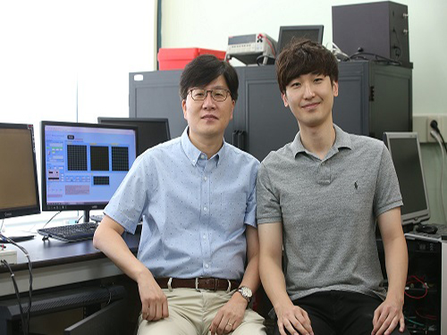
 Transfering Nanowires onto a Flexible Substrate
(from left: PhD Min-Ho Seo and Professor Jun-Bo Yoon)
Boasting excellent physical and chemical properties, nanowires (NWs) are suitable for fabricating flexible electronics; therefore, technology to transfer well-aligned wires plays a crucial role in enhancing performance of the devices. A KAIST research team succeeded in developing NW-transfer technology that is expected to enhance the existing chemical reaction-based NW fabrication technology that has this far showed low performance in applicability and productivity.
NWs, one of the most well-known nanomaterials, have the structural advantage of being small and lightweight. Hence, NW-transfer technology has drawn attention because it can fabricate high-performance, flexible nanodevices with high simplicity and throughput.
A conventional nanowire-fabrication method generally has an irregularity issue since it mixes chemically synthesized nanowires in a solution and randomly distributes the NWs onto flexible substrates. Hence, numerous nanofabrication processes have emerged, and one of them is master-mold-based, which enables the fabrication of highly ordered NW arrays embedded onto substrates in a simple and cost-effective manner, but its employment is limited to only some materials because of its chemistry-based NW-transfer mechanism, which is complex and time consuming. For the successful transfer, it requires that adequate chemicals controlling the chemical interfacial adhesion between the master mold, NWs, and flexible substrate be present.
Here, Professor Jun-Bo Yoon and his team from the School of Electrical Engineering introduced a material-independent mechanical-interlocking-based nanowire-transfer (MINT) method to fabricate ultralong and fully aligned NWs on a large flexible substrate in a highly robust manner.
This method involves sequentially forming a nanosacrificial layer and NWs on a nanograting substrate that becomes the master mold for the transfer, then weakening the structure of the nanosacrificial layer through a dry etching process. The nanosacrificial layer very weakly holds the nanowires on the master mold. Therefore, when using a flexible substrate material, the nanowires are very easily transferred from the master mold to the substrate, just like a piece of tape lifting dust off a carpet.
This technology uses common physical vapor deposition and does not rely on NW materials, making it easy to fabricate NWs onto the flexible substrates.
Using this technology, the team was able to fabricate a variety of metal and metal-oxide NWs, including gold, platinum, and copper – all perfectly aligned on a flexible substrate. They also confirmed that it can be applied to creating stable and applicable devices in everyday life by successfully applying it to flexible heaters and gas sensors.
PhD Min-Ho Seo who led this research said, “We have successfully aligned various metals and semiconductor NWs with excellent physical properties onto flexible substrates and applied them to fabricated devices. As a platform-technology, it will contribute to developing high-performing and stable electronic devices.”
This research was published in ACS Nano on May 24.
Figure 1. Photograph of the fabricated wafer-scale fully aligned and ultralong Au nanowire array on a flexible substrate
2018.09.17 View 6934
Transfering Nanowires onto a Flexible Substrate
(from left: PhD Min-Ho Seo and Professor Jun-Bo Yoon)
Boasting excellent physical and chemical properties, nanowires (NWs) are suitable for fabricating flexible electronics; therefore, technology to transfer well-aligned wires plays a crucial role in enhancing performance of the devices. A KAIST research team succeeded in developing NW-transfer technology that is expected to enhance the existing chemical reaction-based NW fabrication technology that has this far showed low performance in applicability and productivity.
NWs, one of the most well-known nanomaterials, have the structural advantage of being small and lightweight. Hence, NW-transfer technology has drawn attention because it can fabricate high-performance, flexible nanodevices with high simplicity and throughput.
A conventional nanowire-fabrication method generally has an irregularity issue since it mixes chemically synthesized nanowires in a solution and randomly distributes the NWs onto flexible substrates. Hence, numerous nanofabrication processes have emerged, and one of them is master-mold-based, which enables the fabrication of highly ordered NW arrays embedded onto substrates in a simple and cost-effective manner, but its employment is limited to only some materials because of its chemistry-based NW-transfer mechanism, which is complex and time consuming. For the successful transfer, it requires that adequate chemicals controlling the chemical interfacial adhesion between the master mold, NWs, and flexible substrate be present.
Here, Professor Jun-Bo Yoon and his team from the School of Electrical Engineering introduced a material-independent mechanical-interlocking-based nanowire-transfer (MINT) method to fabricate ultralong and fully aligned NWs on a large flexible substrate in a highly robust manner.
This method involves sequentially forming a nanosacrificial layer and NWs on a nanograting substrate that becomes the master mold for the transfer, then weakening the structure of the nanosacrificial layer through a dry etching process. The nanosacrificial layer very weakly holds the nanowires on the master mold. Therefore, when using a flexible substrate material, the nanowires are very easily transferred from the master mold to the substrate, just like a piece of tape lifting dust off a carpet.
This technology uses common physical vapor deposition and does not rely on NW materials, making it easy to fabricate NWs onto the flexible substrates.
Using this technology, the team was able to fabricate a variety of metal and metal-oxide NWs, including gold, platinum, and copper – all perfectly aligned on a flexible substrate. They also confirmed that it can be applied to creating stable and applicable devices in everyday life by successfully applying it to flexible heaters and gas sensors.
PhD Min-Ho Seo who led this research said, “We have successfully aligned various metals and semiconductor NWs with excellent physical properties onto flexible substrates and applied them to fabricated devices. As a platform-technology, it will contribute to developing high-performing and stable electronic devices.”
This research was published in ACS Nano on May 24.
Figure 1. Photograph of the fabricated wafer-scale fully aligned and ultralong Au nanowire array on a flexible substrate
2018.09.17 View 6934 -
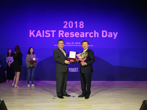 2018 KAIST Research Day Honors Outstanding Research Achievements
(KAIST President Sung-Chul Shin and Professor Jong-Hwan Kim) Professor Jong-Hwan Kim from the School of Electrical Engineering was recognized at the 2018 KAIST Research Day as the Research Grand Prize Awardee. The ten most distinguished research achievements of the past year were also recognized.
The Research Grand Prize recognizes the professor whose comprehensive research performance evaluation indicator was the highest over the past five years. The indicator combines the number of research contracts, IPR and royalty income.
During the May 25th ceremony, Professor Hyochoong Bang from the Department of Aerospace Engineering and Professor In so Kweon from the School of Electrical Engineering also won the Best Research Award prize.
This year, the Research Innovation Award went to Professor Dong Soo Han from the School of Computing. The Research Innovation Award combines scores in the categories of foreign patent registrations, contracts of technological transfer, and income from technology fees, technology consultations, and startups.
The Convergence Research Award was given to Professor Junmo Kim from the School of Electrical Engineering and Professor Hyun Myung from the Department of Civil & Environmental Engineering. The Convergence Research Award recognizes the most outstanding research team that created innovative research results over a one-year period.
President Sung-Chul Shin said, “KAIST has selected the ten most outstanding research achievements of 2017 conducted by our faculty and researchers. All of them demonstrated exceptional creativity, which opens new research paths in each field though their novelty, innovation, and impact.”
KAIST hosts Research Day every year to introduce major research performances at KAIST and share knowledge about the research and development.
During Research Day, KAIST also announced the ten most distinguished research achievements contributed by KAIST professors during the previous year. They are listed below.
▲ High-Speed Motion Core Technology for Magnetic Memory by Professor Kab-Jin Kim from the Department of Physics
▲ A Double Well Potential System by Professor Jaeyoung Byeon from the Department of Mathematical Sciences
▲ Cheap and Efficient Dehydrogenation of Alkanes by Professor Mu-Hyun Baik from the Department of Chemistry
▲ A Dynamic LPS Transfer Mechanism for Innate Immune Activation by Professor Ho Min Kim from the Graduate School of Medical Science and Engineering
▲ A Memristive Functional Device and Circuit on Fabric for Fibertronics by Professor Yang-Kyu Choi and Professor Sung-Yool Choi from the School of Electrical Engineering
▲ A Hippocampal Morphology Study Based on a Progressive Template Deformable Model by Professor Jinah Park from the School of Computing
▲ The Development of a 6-DOF Dynamic Response Measurement System for Civil Infrastructure Monitoring by Professor Hoon Sohn from the Department of Civil and Environmental Engineering
▲ Cooperative Tumour Cell Membrane Targeted Phototherapy by Professor Ji-Ho Park from the Department of Bio and Brain Engineering
▲ HUMICOTTA: A 3D-Printed Terracotta Humidifier by Professor Sangmin Bae from the Department of Industrial Design
▲ Ultrathin, Cross-Linked Ionic Polymer Thin Films by Professor Sung Gap Im from the Department of Chemical and Biomolecular Engineering
2018.05.28 View 13289
2018 KAIST Research Day Honors Outstanding Research Achievements
(KAIST President Sung-Chul Shin and Professor Jong-Hwan Kim) Professor Jong-Hwan Kim from the School of Electrical Engineering was recognized at the 2018 KAIST Research Day as the Research Grand Prize Awardee. The ten most distinguished research achievements of the past year were also recognized.
The Research Grand Prize recognizes the professor whose comprehensive research performance evaluation indicator was the highest over the past five years. The indicator combines the number of research contracts, IPR and royalty income.
During the May 25th ceremony, Professor Hyochoong Bang from the Department of Aerospace Engineering and Professor In so Kweon from the School of Electrical Engineering also won the Best Research Award prize.
This year, the Research Innovation Award went to Professor Dong Soo Han from the School of Computing. The Research Innovation Award combines scores in the categories of foreign patent registrations, contracts of technological transfer, and income from technology fees, technology consultations, and startups.
The Convergence Research Award was given to Professor Junmo Kim from the School of Electrical Engineering and Professor Hyun Myung from the Department of Civil & Environmental Engineering. The Convergence Research Award recognizes the most outstanding research team that created innovative research results over a one-year period.
President Sung-Chul Shin said, “KAIST has selected the ten most outstanding research achievements of 2017 conducted by our faculty and researchers. All of them demonstrated exceptional creativity, which opens new research paths in each field though their novelty, innovation, and impact.”
KAIST hosts Research Day every year to introduce major research performances at KAIST and share knowledge about the research and development.
During Research Day, KAIST also announced the ten most distinguished research achievements contributed by KAIST professors during the previous year. They are listed below.
▲ High-Speed Motion Core Technology for Magnetic Memory by Professor Kab-Jin Kim from the Department of Physics
▲ A Double Well Potential System by Professor Jaeyoung Byeon from the Department of Mathematical Sciences
▲ Cheap and Efficient Dehydrogenation of Alkanes by Professor Mu-Hyun Baik from the Department of Chemistry
▲ A Dynamic LPS Transfer Mechanism for Innate Immune Activation by Professor Ho Min Kim from the Graduate School of Medical Science and Engineering
▲ A Memristive Functional Device and Circuit on Fabric for Fibertronics by Professor Yang-Kyu Choi and Professor Sung-Yool Choi from the School of Electrical Engineering
▲ A Hippocampal Morphology Study Based on a Progressive Template Deformable Model by Professor Jinah Park from the School of Computing
▲ The Development of a 6-DOF Dynamic Response Measurement System for Civil Infrastructure Monitoring by Professor Hoon Sohn from the Department of Civil and Environmental Engineering
▲ Cooperative Tumour Cell Membrane Targeted Phototherapy by Professor Ji-Ho Park from the Department of Bio and Brain Engineering
▲ HUMICOTTA: A 3D-Printed Terracotta Humidifier by Professor Sangmin Bae from the Department of Industrial Design
▲ Ultrathin, Cross-Linked Ionic Polymer Thin Films by Professor Sung Gap Im from the Department of Chemical and Biomolecular Engineering
2018.05.28 View 13289 -
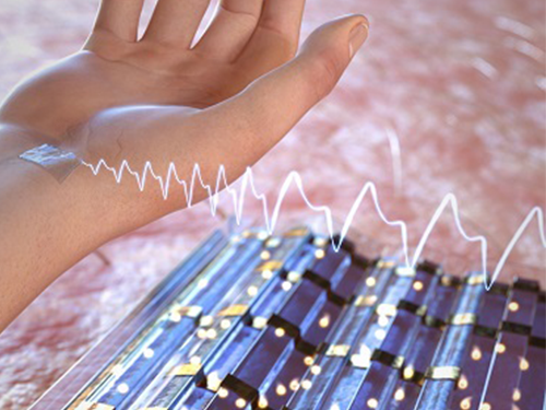
 Get Treatment Anywhere and Any Time with Wearable PBM Patch
(PhD Candidate Yongmin Jeon)
There have been many cases in which OLEDs are applied to electronic devices, and now they have even been extended to therapeutic fields. A KAIST research team succeeded in developing a wearable photobiomodulation (PBM) patch to treat wounds. This technology will allow injuries to be treated regardless of location or time.
Professor KyungCheol Choi from the School of Electrical Engineering, in collaboration with Seoul National University Bundang Hospital’s team, conducted research on PBMs which are a clinical method widely used in hospitals. They are considered to be a safe, noninvasive, and nonsurgical method that require relatively low light power.
Conventionally, light-emitting diodes (LEDs) have been used in PBM applications; however, LED devices are usually inflexible and difficult to irradiate light uniformly. They may also produce localized heat. Due to these constraints, it was difficult to enhance the clinical effects of LED devices as they cannot stick to the human body.
Choi’s team developed a wearable patch using flexible OLEDs, allowing people to be treated outside of hospitals. A thin film has been developed for the patch, containing not only flexible OLEDs but also batteries and anti-superheating devices.
Moreover, its thickness is less than 1mm and its weight is less than 1g. This lightweight and ultra-thin patch with a bending radius is 20mm can be used more than 300 hours.
These patches are usable at a temperature below 42℃ to eliminate the risk of low-temperature burns. They also meet the safety regulations of the International Organization for Standardization (ISO) at red wavelengths (600–700 nm).
The wearable PBM patches showed excellent effects with in vitro wounds because they stimulated cell proliferation over 58% of control as well as cell migration over 46% of control under various conditions.
Yongmin Jeon, who led this research, said, “The wearable PBM is effective and convenient, so people can simply purchase it at a pharmacy without having to visit a hospital. If we can adjust the power and wavelength of the OLEDs, its application can be extended to skin care, cancer treatment, Alzheimer’s disease treatment, and mental healthcare.”
Professor Choi added, “We have applied the advantages of flexible OLEDs, which are often used for fabricating displays, to PBMs. This technology will open the way to commercialize portable and highly-efficient wearable photobiomodulation devices.”
This research was published in the front cover of Advanced Materials Technologies on May, 2018.
Figure 1. The patch attached to a human face, a hand and examples of treatment applications
Figure 2. The migration of cells into the scratched area
2018.05.25 View 8134
Get Treatment Anywhere and Any Time with Wearable PBM Patch
(PhD Candidate Yongmin Jeon)
There have been many cases in which OLEDs are applied to electronic devices, and now they have even been extended to therapeutic fields. A KAIST research team succeeded in developing a wearable photobiomodulation (PBM) patch to treat wounds. This technology will allow injuries to be treated regardless of location or time.
Professor KyungCheol Choi from the School of Electrical Engineering, in collaboration with Seoul National University Bundang Hospital’s team, conducted research on PBMs which are a clinical method widely used in hospitals. They are considered to be a safe, noninvasive, and nonsurgical method that require relatively low light power.
Conventionally, light-emitting diodes (LEDs) have been used in PBM applications; however, LED devices are usually inflexible and difficult to irradiate light uniformly. They may also produce localized heat. Due to these constraints, it was difficult to enhance the clinical effects of LED devices as they cannot stick to the human body.
Choi’s team developed a wearable patch using flexible OLEDs, allowing people to be treated outside of hospitals. A thin film has been developed for the patch, containing not only flexible OLEDs but also batteries and anti-superheating devices.
Moreover, its thickness is less than 1mm and its weight is less than 1g. This lightweight and ultra-thin patch with a bending radius is 20mm can be used more than 300 hours.
These patches are usable at a temperature below 42℃ to eliminate the risk of low-temperature burns. They also meet the safety regulations of the International Organization for Standardization (ISO) at red wavelengths (600–700 nm).
The wearable PBM patches showed excellent effects with in vitro wounds because they stimulated cell proliferation over 58% of control as well as cell migration over 46% of control under various conditions.
Yongmin Jeon, who led this research, said, “The wearable PBM is effective and convenient, so people can simply purchase it at a pharmacy without having to visit a hospital. If we can adjust the power and wavelength of the OLEDs, its application can be extended to skin care, cancer treatment, Alzheimer’s disease treatment, and mental healthcare.”
Professor Choi added, “We have applied the advantages of flexible OLEDs, which are often used for fabricating displays, to PBMs. This technology will open the way to commercialize portable and highly-efficient wearable photobiomodulation devices.”
This research was published in the front cover of Advanced Materials Technologies on May, 2018.
Figure 1. The patch attached to a human face, a hand and examples of treatment applications
Figure 2. The migration of cells into the scratched area
2018.05.25 View 8134 -
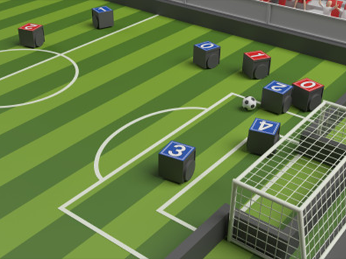 KAIST Welcomes Global Participants to AI World Cup 2018
KAIST will host the AI (Artificial Intelligence) World Cup 2018 in August, and this time it is open to the international community. AI World Cup 2018 will be a very exciting challenge for extending the limit of academic and industrial applications based on AI technology.
KAIST, after launching its AI World Cup 2017 for domestic participants, is now hosting the AI World Cup 2018 for everyone. The AI World Cup will be comprised of three events: 1) Five on five AI Soccer 2) AI Commentator and 3) AI Reporter. Winner of each category, runner-up of AI Soccer, and 2nd runner-up of AI Soccer will receive awards with cash prizes.
For AI Soccer in which AI controlled robots team up to compete, the preliminary rounds will be held in July in a league format, and the final rounds will be played on August 20-22.
For AI Commentator and AI Reporter, eight finalists will be selected for each category based on scoring criteria, and their performance will be evaluated by the judges to select the winner from each category on August 22.
During the final rounds, a variety of events will also take place at KAIST, including tutorial sessions on AI technology, a poster session where students present their research works on AI, not necessarily limited to the scope of AI Soccer, AI Commentator, and AI Reporter, and panel discussions by prominent experts in the field of AI.
Moreover, renowned experts on AI will deliver their keynote addresses. The Cyberbotics CEO Olivier Michel will address his keynote speech on the topic ‘Simulation benchmarks and competitions: a fundamental tool to foster robotics research.’
The AI World Cup was established by the College of Engineering at KAIST to show that AI technology can be further extended to sports, soccer in particular.
Professor Jong-Hwan Kim, the inventor of AI World Cup and chairman of the organizing committee said, “I hope that this event will offer a great chance to develop AI technology for use in the coming years. I wish many people can enjoy the AI World Cup 2018. I would recommend that prospective teams not worry about the technical barrier when deciding whether to participate in the games. Participants from academia and industry can test whether their code runs well in the competition simulator; this way, they will know their level of play and perhaps they can further develop their algorithms.”
“We will also broadcast the final round of AI Soccer online so that people in remote areas can also enjoy watching the games. I am looking forward to seeing all of you at the AI World Cup. Any participant with a passion to prove excellence in AI technology is welcomed with open arms,” he added.
Anyone interested in the AI World Cup 2018 can register online via aiworldcup.org . Registration starts from April 1. The deadline for registration and final code submission is June 30.
(Cubical players in the figure for domestic AI Soccer competition have been replaced with cylindrical players for more agile movements while playing)
(Opening ceremony of AI World Cup 2017)
(Trophy and prize)
(Interview of participant)
(Casters commentating on game playing)
2018.03.30 View 9465
KAIST Welcomes Global Participants to AI World Cup 2018
KAIST will host the AI (Artificial Intelligence) World Cup 2018 in August, and this time it is open to the international community. AI World Cup 2018 will be a very exciting challenge for extending the limit of academic and industrial applications based on AI technology.
KAIST, after launching its AI World Cup 2017 for domestic participants, is now hosting the AI World Cup 2018 for everyone. The AI World Cup will be comprised of three events: 1) Five on five AI Soccer 2) AI Commentator and 3) AI Reporter. Winner of each category, runner-up of AI Soccer, and 2nd runner-up of AI Soccer will receive awards with cash prizes.
For AI Soccer in which AI controlled robots team up to compete, the preliminary rounds will be held in July in a league format, and the final rounds will be played on August 20-22.
For AI Commentator and AI Reporter, eight finalists will be selected for each category based on scoring criteria, and their performance will be evaluated by the judges to select the winner from each category on August 22.
During the final rounds, a variety of events will also take place at KAIST, including tutorial sessions on AI technology, a poster session where students present their research works on AI, not necessarily limited to the scope of AI Soccer, AI Commentator, and AI Reporter, and panel discussions by prominent experts in the field of AI.
Moreover, renowned experts on AI will deliver their keynote addresses. The Cyberbotics CEO Olivier Michel will address his keynote speech on the topic ‘Simulation benchmarks and competitions: a fundamental tool to foster robotics research.’
The AI World Cup was established by the College of Engineering at KAIST to show that AI technology can be further extended to sports, soccer in particular.
Professor Jong-Hwan Kim, the inventor of AI World Cup and chairman of the organizing committee said, “I hope that this event will offer a great chance to develop AI technology for use in the coming years. I wish many people can enjoy the AI World Cup 2018. I would recommend that prospective teams not worry about the technical barrier when deciding whether to participate in the games. Participants from academia and industry can test whether their code runs well in the competition simulator; this way, they will know their level of play and perhaps they can further develop their algorithms.”
“We will also broadcast the final round of AI Soccer online so that people in remote areas can also enjoy watching the games. I am looking forward to seeing all of you at the AI World Cup. Any participant with a passion to prove excellence in AI technology is welcomed with open arms,” he added.
Anyone interested in the AI World Cup 2018 can register online via aiworldcup.org . Registration starts from April 1. The deadline for registration and final code submission is June 30.
(Cubical players in the figure for domestic AI Soccer competition have been replaced with cylindrical players for more agile movements while playing)
(Opening ceremony of AI World Cup 2017)
(Trophy and prize)
(Interview of participant)
(Casters commentating on game playing)
2018.03.30 View 9465 -
 Recognizing Seven Different Face Emotions on a Mobile Platform
(Professor Hoi-Jun Yoo)
A KAIST research team succeeded in achieving face emotion recognition on a mobile platform by developing an AI semiconductor IC that processes two neural networks on a single chip.
Professor Hoi-Jun Yoo and his team (Primary researcher: Jinmook Lee Ph. D. student) from the School of Electrical Engineering developed a unified deep neural network processing unit (UNPU).
Deep learning is a technology for machine learning based on artificial neural networks, which allows a computer to learn by itself, just like a human.
The developed chip adjusts the weight precision (from 1 bit to 16 bit) of a neural network inside of the semiconductor in order to optimize energy efficiency and accuracy. With a single chip, it can process a convolutional neural network (CNN) and recurrent neural network (RNN) simultaneously. CNN is used for categorizing and recognizing images while RNN is for action recognition and speech recognition, such as time-series information.
Moreover, it enables an adjustment in energy efficiency and accuracy dynamically while recognizing objects. To realize mobile AI technology, it needs to process high-speed operations with low energy, otherwise the battery can run out quickly due to processing massive amounts of information at once. According to the team, this chip has better operation performance compared to world-class level mobile AI chips such as Google TPU. The energy efficiency of the new chip is 4 times higher than the TPU.
In order to demonstrate its high performance, the team installed UNPU in a smartphone to facilitate automatic face emotion recognition on the smartphone. This system displays a user’s emotions in real time. The research results for this system were presented at the 2018 International Solid-State Circuits Conference (ISSCC) in San Francisco on February 13.
Professor Yoo said, “We have developed a semiconductor that accelerates with low power requirements in order to realize AI on mobile platforms. We are hoping that this technology will be applied in various areas, such as object recognition, emotion recognition, action recognition, and automatic translation. Within one year, we will commercialize this technology.”
2018.03.09 View 7725
Recognizing Seven Different Face Emotions on a Mobile Platform
(Professor Hoi-Jun Yoo)
A KAIST research team succeeded in achieving face emotion recognition on a mobile platform by developing an AI semiconductor IC that processes two neural networks on a single chip.
Professor Hoi-Jun Yoo and his team (Primary researcher: Jinmook Lee Ph. D. student) from the School of Electrical Engineering developed a unified deep neural network processing unit (UNPU).
Deep learning is a technology for machine learning based on artificial neural networks, which allows a computer to learn by itself, just like a human.
The developed chip adjusts the weight precision (from 1 bit to 16 bit) of a neural network inside of the semiconductor in order to optimize energy efficiency and accuracy. With a single chip, it can process a convolutional neural network (CNN) and recurrent neural network (RNN) simultaneously. CNN is used for categorizing and recognizing images while RNN is for action recognition and speech recognition, such as time-series information.
Moreover, it enables an adjustment in energy efficiency and accuracy dynamically while recognizing objects. To realize mobile AI technology, it needs to process high-speed operations with low energy, otherwise the battery can run out quickly due to processing massive amounts of information at once. According to the team, this chip has better operation performance compared to world-class level mobile AI chips such as Google TPU. The energy efficiency of the new chip is 4 times higher than the TPU.
In order to demonstrate its high performance, the team installed UNPU in a smartphone to facilitate automatic face emotion recognition on the smartphone. This system displays a user’s emotions in real time. The research results for this system were presented at the 2018 International Solid-State Circuits Conference (ISSCC) in San Francisco on February 13.
Professor Yoo said, “We have developed a semiconductor that accelerates with low power requirements in order to realize AI on mobile platforms. We are hoping that this technology will be applied in various areas, such as object recognition, emotion recognition, action recognition, and automatic translation. Within one year, we will commercialize this technology.”
2018.03.09 View 7725 -
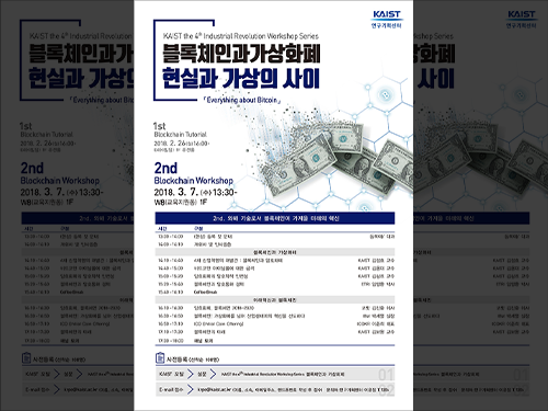 Blockchain and Cryptocurrency: Between Reality and Virtuality
A workshop on blockchain and cryptocurrency, one of the 4th Industrial Revolution Workshop Series, was held at the KAIST main campus on March 7.
Experts from industry, academia, and research gathered and shared their opinions about blockchain technology, which is currently gaining huge attention along with cryptocurrency.
During the workshop, four KAIST professors and four experts from institutes and business examined the scope on the possibility of blockchain, technology for the Fourth Industrial Revolution.
Moreover, they discussed a variety of issues including mining, wallets, cryptocurrency, information security, smart contracts, and ICOs.
In a previous blockchain tutorial, Professor Yongdae Kim from the School of Electrical Engineering at KAIST and Professor Hyoungshick Kim from Sungkyunkwan University opened up a blockchain tutorial which provided a technical understanding of blockchain, such as the birth of cryptocurrency, algorithm design, and exchange methods.
Professor Jungho Kim, who is in charge of this event, said, “This workshop will broaden the understanding of blockchain, which can provide a foundation for a national growth engine.”
2018.03.07 View 9103
Blockchain and Cryptocurrency: Between Reality and Virtuality
A workshop on blockchain and cryptocurrency, one of the 4th Industrial Revolution Workshop Series, was held at the KAIST main campus on March 7.
Experts from industry, academia, and research gathered and shared their opinions about blockchain technology, which is currently gaining huge attention along with cryptocurrency.
During the workshop, four KAIST professors and four experts from institutes and business examined the scope on the possibility of blockchain, technology for the Fourth Industrial Revolution.
Moreover, they discussed a variety of issues including mining, wallets, cryptocurrency, information security, smart contracts, and ICOs.
In a previous blockchain tutorial, Professor Yongdae Kim from the School of Electrical Engineering at KAIST and Professor Hyoungshick Kim from Sungkyunkwan University opened up a blockchain tutorial which provided a technical understanding of blockchain, such as the birth of cryptocurrency, algorithm design, and exchange methods.
Professor Jungho Kim, who is in charge of this event, said, “This workshop will broaden the understanding of blockchain, which can provide a foundation for a national growth engine.”
2018.03.07 View 9103 -
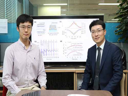
 Low-power, Flexible Memristor Circuit for Mobile and Wearable Devices
(from left: Yunyong Nam, Professor Sung-Yool Choi and Byung Chul Jang)
A KAIST research team succeeded in developing an energy efficient, nonvolatile logic-in-memory circuit by using a memristor. This novel technology can be used as an energy efficient computing architecture for battery-powered flexible electronic systems, such as mobile and wearable devices.
Professor Sung-Yool Choi from the School of Electrical Engineering and Professor Sang-Hee Ko Park from the Department of Materials Science and Engineering developed a memristive nonvolatile logic-in-memory circuit.
Transistor-based conventional electronic systems have issues with battery supply and a long standby period due to their volatile computing architecture. The standby power consumption caused by subthreshold leakage current limits their potential applications for mobile electronic devices. Also, their physical separation of memory and processor causes power consumption and time delay during data transfer.
In order to solve this problem, the team developed a logic-in-memory circuit that enables data storage as well as logic operation simultaneously. It can minimize energy consumption and time delay because it does not require data transfer between memory and processor.
The team employed nonvolatile, polymer-based memristors and flexible back-to-back Schottky diode selector devices on plastic substrates. Unlike the conventional architecture, this memristive nonvolatile logic-in-memory is a novel computing architecture that consumes a minimal amount of standby power. This one-selector-one memristor (1S-1M) solved the issue of undesirable leakage currents, known as ‘sneak currents’.
They also implemented single-instruction multiple-data (SIMD) to calculate multiple values at once.
The proposed parallel computing method using a memristive nonvolatile logic-in-memory circuit can provide a low-power circuit platform for battery-powered flexible electronic systems with a variety of potential applications.
Professor Choi said, “Flexible logic-in-memory circuits integrating memristor and selector device can provide flexibility, low power, memory with logic functions. This will be a core technology that will bring innovation to mobile and wearable electronic systems.”
This research, collaborated with Ph.D. candidates Byung Chul Jang and Yunyong Nam, was published and chosen as the cover of Advanced Functional Materials on January 10.
Figure 1. Cover of the Advanced Functional Materials
Figure 2. Schematic illustration and cross-sectional TEM image of flexible memristive nonvolatile logic-in-memory circuit
Figure 3. Test performance
Figure 4. Parallel logic operation within 1S-1M memristor array
2018.02.21 View 7247
Low-power, Flexible Memristor Circuit for Mobile and Wearable Devices
(from left: Yunyong Nam, Professor Sung-Yool Choi and Byung Chul Jang)
A KAIST research team succeeded in developing an energy efficient, nonvolatile logic-in-memory circuit by using a memristor. This novel technology can be used as an energy efficient computing architecture for battery-powered flexible electronic systems, such as mobile and wearable devices.
Professor Sung-Yool Choi from the School of Electrical Engineering and Professor Sang-Hee Ko Park from the Department of Materials Science and Engineering developed a memristive nonvolatile logic-in-memory circuit.
Transistor-based conventional electronic systems have issues with battery supply and a long standby period due to their volatile computing architecture. The standby power consumption caused by subthreshold leakage current limits their potential applications for mobile electronic devices. Also, their physical separation of memory and processor causes power consumption and time delay during data transfer.
In order to solve this problem, the team developed a logic-in-memory circuit that enables data storage as well as logic operation simultaneously. It can minimize energy consumption and time delay because it does not require data transfer between memory and processor.
The team employed nonvolatile, polymer-based memristors and flexible back-to-back Schottky diode selector devices on plastic substrates. Unlike the conventional architecture, this memristive nonvolatile logic-in-memory is a novel computing architecture that consumes a minimal amount of standby power. This one-selector-one memristor (1S-1M) solved the issue of undesirable leakage currents, known as ‘sneak currents’.
They also implemented single-instruction multiple-data (SIMD) to calculate multiple values at once.
The proposed parallel computing method using a memristive nonvolatile logic-in-memory circuit can provide a low-power circuit platform for battery-powered flexible electronic systems with a variety of potential applications.
Professor Choi said, “Flexible logic-in-memory circuits integrating memristor and selector device can provide flexibility, low power, memory with logic functions. This will be a core technology that will bring innovation to mobile and wearable electronic systems.”
This research, collaborated with Ph.D. candidates Byung Chul Jang and Yunyong Nam, was published and chosen as the cover of Advanced Functional Materials on January 10.
Figure 1. Cover of the Advanced Functional Materials
Figure 2. Schematic illustration and cross-sectional TEM image of flexible memristive nonvolatile logic-in-memory circuit
Figure 3. Test performance
Figure 4. Parallel logic operation within 1S-1M memristor array
2018.02.21 View 7247 -
 A Parallel MRI Method Accelerating Imaging Time Proposed
KAIST researchers proposed new technology that reduces MRI (magnetic resonance imaging) acquisition time to less than a sixth of the conventional method. They made a reconstruction method using machine learning of multilayer perception (MLP) algorithm to accelerate imaging time.
High-quality image can be reconstructed from subsampled data using the proposed method. This method can be further applied to various k-space subsampling patterns in a phase encoding direction, and its processing can be performed in real time.
The research, led by Professor Hyun Wook Park from the Department of Electrical Engineering, was described in Medical Physics as the cover paper last December. Ph.D. candidate Kinam Kwon is the first author.
MRI is an imaging technique that allows various contrasts of soft tissues without using radioactivity. Since MRI could image not only anatomical structures, but also functional and physiological features, it is widely used in medical diagnoses. However, one of the major shortcomings of MRI is its long imaging time. It induces patients’ discomfort, which is closely related to voluntary and involuntary motions, thereby deteriorating the quality of the MR images. In addition, lengthy imaging times limit the system’s throughput, which results in the long waiting times of patients as well as the increased medical expenses.
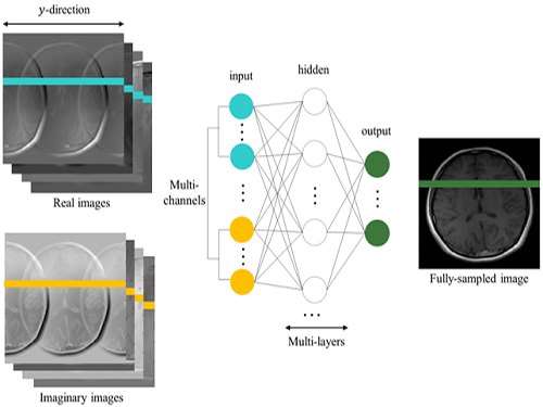
To reconstruct MR images from subsampled data, the team applied the MLP to reduce aliasing artifacts generated by subsampling in k-space. The MLP is learned from training data to map aliased input images into desired alias-free images. The input of the MLP is all voxels in the aliased lines of multichannel real and imaginary images from the subsampled k-space data, and the desired output is all voxels in the corresponding alias-free line of the root-sum-of-squares of multichannel images from fully sampled k-space data. Aliasing artifacts in an image reconstructed from subsampled data were reduced by line-by-line processing of the learned MLP architecture.
Reconstructed images from the proposed method are better than those from compared methods in terms of normalized root-mean-square error. The proposed method can be applied to image reconstruction for any k-space subsampling patterns in a phase encoding direction. Moreover, to further reduce the reconstruction time, it is easily implemented by parallel processing.
To address the aliasing artifact phenomenon, the team employed a parallel imaging technique using several receiver coils of various sensitivities and a compressed sensing technique using sparsity of signals.
Existing methods are heavily affected by sub-sampling patterns, but the team’s technique is applicable for various sub-sampling patterns, resulting in superior reconstructed images compared to existing methods, as well as allowing real-time reconstruction.
Professor Park said, "MRIs have become essential equipment in clinical diagnosis. However, the time consumption and the cost led to many inconveniences." He continued, "This method using machine learning could greatly improve the patients’ satisfaction with medical service." This research was funded by the Ministry of Science and ICT.
(Firgure 1. Cover of Medical Physics for December 2017)
(Figure 2. Concept map for the suggested network)
(Figure 3. Concept map for conventional MRI image acquisition and accelerated image acquisiton)
2018.01.16 View 7014
A Parallel MRI Method Accelerating Imaging Time Proposed
KAIST researchers proposed new technology that reduces MRI (magnetic resonance imaging) acquisition time to less than a sixth of the conventional method. They made a reconstruction method using machine learning of multilayer perception (MLP) algorithm to accelerate imaging time.
High-quality image can be reconstructed from subsampled data using the proposed method. This method can be further applied to various k-space subsampling patterns in a phase encoding direction, and its processing can be performed in real time.
The research, led by Professor Hyun Wook Park from the Department of Electrical Engineering, was described in Medical Physics as the cover paper last December. Ph.D. candidate Kinam Kwon is the first author.
MRI is an imaging technique that allows various contrasts of soft tissues without using radioactivity. Since MRI could image not only anatomical structures, but also functional and physiological features, it is widely used in medical diagnoses. However, one of the major shortcomings of MRI is its long imaging time. It induces patients’ discomfort, which is closely related to voluntary and involuntary motions, thereby deteriorating the quality of the MR images. In addition, lengthy imaging times limit the system’s throughput, which results in the long waiting times of patients as well as the increased medical expenses.
To reconstruct MR images from subsampled data, the team applied the MLP to reduce aliasing artifacts generated by subsampling in k-space. The MLP is learned from training data to map aliased input images into desired alias-free images. The input of the MLP is all voxels in the aliased lines of multichannel real and imaginary images from the subsampled k-space data, and the desired output is all voxels in the corresponding alias-free line of the root-sum-of-squares of multichannel images from fully sampled k-space data. Aliasing artifacts in an image reconstructed from subsampled data were reduced by line-by-line processing of the learned MLP architecture.
Reconstructed images from the proposed method are better than those from compared methods in terms of normalized root-mean-square error. The proposed method can be applied to image reconstruction for any k-space subsampling patterns in a phase encoding direction. Moreover, to further reduce the reconstruction time, it is easily implemented by parallel processing.
To address the aliasing artifact phenomenon, the team employed a parallel imaging technique using several receiver coils of various sensitivities and a compressed sensing technique using sparsity of signals.
Existing methods are heavily affected by sub-sampling patterns, but the team’s technique is applicable for various sub-sampling patterns, resulting in superior reconstructed images compared to existing methods, as well as allowing real-time reconstruction.
Professor Park said, "MRIs have become essential equipment in clinical diagnosis. However, the time consumption and the cost led to many inconveniences." He continued, "This method using machine learning could greatly improve the patients’ satisfaction with medical service." This research was funded by the Ministry of Science and ICT.
(Firgure 1. Cover of Medical Physics for December 2017)
(Figure 2. Concept map for the suggested network)
(Figure 3. Concept map for conventional MRI image acquisition and accelerated image acquisiton)
2018.01.16 View 7014 -
 Fiber OLEDs, Thinner Than a Hair
(Seonil Kwon, PhD Candidate)
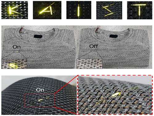
Professor Kyung Cheol Choi from the School of Electrical Engineering and his team succeeded in fabricating highly efficient Organic Light-Emitting Diodes (OLEDs) on an ultra-thin fiber.
The team expects the technology, which produces high-efficiency, long-lasting OLEDs, can be widely utilized in wearable displays.
Existing fiber-based wearable displays’ OLEDs show much lower performance compared to those fabricated on planar substrates. This low performance caused a limitation for applying it to actual wearable displays.
In order to solve this problem, the team designed a structure of OLEDs compatible to fiber and used a dip-coating method in a three-dimensional structure of fibers. Through this method, the team successfully developed efficient OLEDs that are designed to last a lifetime and are still equivalent to those on planar substrates.
The team identified that solution process planar OLEDs can be applied to fibers without any reduction in performance through the technology. This fiber OLEDs exhibited luminance and current efficiency values of over 10,000 cd/m^2(candela/square meter) and 11 cd/A (candela/ampere).
The team also verified that the fiber OLEDs withstood tensile strains of up to 4.3% while retaining more than 90% of their current efficiency. In addition, they could be woven into textiles and knitted clothes without causing any problems.
Moreover, the technology allows for fabricating OLEDs on fibers with diameters ranging from 300㎛ down to 90㎛, thinner than a human hair, which attests to the scalability of the proposed fabrication scheme.
Noting that every process is carried out at a low temperature (~105℃), fibers vulnerable to high temperatures can also employ this fabrication scheme.
Professor Choi said, “Existing fiber-based wearable displays had limitations for applicability due to their low performance. However, this technology can fabricate OLEDs with high performance on fibers. This simple, low-cost process opens a way to commercialize fiber-based wearable displays.”
This research led by a PhD candidate Seonil Kwon was published online in the international journal for nanoscience, Nano Letters, on December 6.
(Fiber-based OLEDs woven into knitted clothes)
This work was funded by the Engineering Research Center of Excellence Program (Grant No. NRF-2017R1A5A1014708) and Nano-Material Technology Development Program (Grant No. NRF-2016M3A7B4910635) by the National Research Foundation of Korea, the Ministry of Science and ICT of Korea.
2018.01.09 View 14662
Fiber OLEDs, Thinner Than a Hair
(Seonil Kwon, PhD Candidate)
Professor Kyung Cheol Choi from the School of Electrical Engineering and his team succeeded in fabricating highly efficient Organic Light-Emitting Diodes (OLEDs) on an ultra-thin fiber.
The team expects the technology, which produces high-efficiency, long-lasting OLEDs, can be widely utilized in wearable displays.
Existing fiber-based wearable displays’ OLEDs show much lower performance compared to those fabricated on planar substrates. This low performance caused a limitation for applying it to actual wearable displays.
In order to solve this problem, the team designed a structure of OLEDs compatible to fiber and used a dip-coating method in a three-dimensional structure of fibers. Through this method, the team successfully developed efficient OLEDs that are designed to last a lifetime and are still equivalent to those on planar substrates.
The team identified that solution process planar OLEDs can be applied to fibers without any reduction in performance through the technology. This fiber OLEDs exhibited luminance and current efficiency values of over 10,000 cd/m^2(candela/square meter) and 11 cd/A (candela/ampere).
The team also verified that the fiber OLEDs withstood tensile strains of up to 4.3% while retaining more than 90% of their current efficiency. In addition, they could be woven into textiles and knitted clothes without causing any problems.
Moreover, the technology allows for fabricating OLEDs on fibers with diameters ranging from 300㎛ down to 90㎛, thinner than a human hair, which attests to the scalability of the proposed fabrication scheme.
Noting that every process is carried out at a low temperature (~105℃), fibers vulnerable to high temperatures can also employ this fabrication scheme.
Professor Choi said, “Existing fiber-based wearable displays had limitations for applicability due to their low performance. However, this technology can fabricate OLEDs with high performance on fibers. This simple, low-cost process opens a way to commercialize fiber-based wearable displays.”
This research led by a PhD candidate Seonil Kwon was published online in the international journal for nanoscience, Nano Letters, on December 6.
(Fiber-based OLEDs woven into knitted clothes)
This work was funded by the Engineering Research Center of Excellence Program (Grant No. NRF-2017R1A5A1014708) and Nano-Material Technology Development Program (Grant No. NRF-2016M3A7B4910635) by the National Research Foundation of Korea, the Ministry of Science and ICT of Korea.
2018.01.09 View 14662 -
 Ultra-Low Power Flexible Memory Using 2D Materials
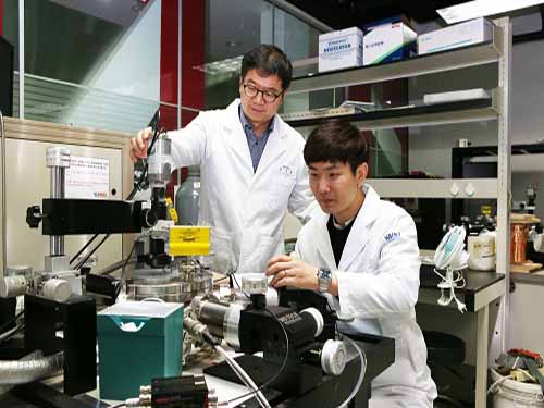
(Professor Choi and Ph.D. candidate Jang)
KAIST research team led by Professor Sung-Yool Choi at School of Electrical Engineering and Professor Sung Gap Im at the Department of Chemical and Biomolecular Engineering developed high-density, ultra-low power, non-volatile, flexible memory technology using 2D materials. The team used ultrathin molybdenum disulfide (MoS2) with atomic-scale thickness as the channel material and high-performance polymeric insulator film as the tunneling dielectric material. This research was published on the cover of Advanced Functional Materials on November 17. KAIST graduate Myung Hun Woo, a researcher at Samsung Electronics and Ph.D. candidate Byung Chul Jang are first authors.
The surge of new technologies such as Internet of Things (IoT), Artificial Intelligence (AI), and cloud server led to the paradigm shift from processor-centric computing to memory-centric computing in the industry, as well as the increase in demand of wearable devices. This led to an increased need for high-density, ultra-low power, non-volatile flexible memory. In particular, ultrathin MoS2 as semiconductor material has been recently regarded as post-silicon material. This is due to its ultrathin thickness of atomic-scale which suppresses short channel effect observed in conventional silicon material, leading to advantages in high- density and low-power consumption. Further, this thickness allows the material to be flexible, and thus the material is applicable to wearable devices.
However, due to the dangling-bond free surface of MoS2 semiconductor material, it is difficult to deposit the thin insulator film to be uniform and stable over a large area via the conventional atomic layer deposition process. Further, the currently used solution process makes it difficult to deposit uniformly low dielectric constant (k) polymeric insulator film with sub-10 nm thickness on a large area, thus indicating that the memory device utilizing the conventional solution-processed polymer insulator film cannot be operated at low-operating voltage and is not compatible with photolithography.
The research team tried to overcome the hurdles and develop high-density, ultra-low power, non-volatile flexible memory by employing a low-temperature, solvent-free, and all-dry vapor phase technique named initiated chemical vapor deposition (iCVD) process. Using iCVD process, tunneling polymeric insulator film with 10 nm thickness was deposited uniformly on MoS2 semiconductor material without being restricted by the dangling bond-free surface of MoS2. The team observed that the newly developed MoS2-based non-volatile memory can be operated at low-voltage (around 10V), in contrast to the conventional MoS2-based non-volatile memory that requires over 20V.
Professor Choi said, “As the basis for the Fourth Industrial revolution technologies including AI and IoT, semiconductor device technology needs to have characteristics of low-power and flexibility, in clear contrast to conventional memory devices.” He continued, “This new technology is significant in developing source technology in terms of materials, processes, and devices to contribute to achieve these characteristics.”
This research was supported by the Global Frontier Center for Advanced Soft Electronics and the Creative Materials Discovery Program by funded the National Research Foundation of Korea of Ministry of Science and ICT.
( Figure 1. Cover of Advanced Functional Materials)
(Figure 2. Concept map for the developed non-volatile memory material and high-resolution transmission electron microscopy image for material cross-section )
2018.01.02 View 10614
Ultra-Low Power Flexible Memory Using 2D Materials
(Professor Choi and Ph.D. candidate Jang)
KAIST research team led by Professor Sung-Yool Choi at School of Electrical Engineering and Professor Sung Gap Im at the Department of Chemical and Biomolecular Engineering developed high-density, ultra-low power, non-volatile, flexible memory technology using 2D materials. The team used ultrathin molybdenum disulfide (MoS2) with atomic-scale thickness as the channel material and high-performance polymeric insulator film as the tunneling dielectric material. This research was published on the cover of Advanced Functional Materials on November 17. KAIST graduate Myung Hun Woo, a researcher at Samsung Electronics and Ph.D. candidate Byung Chul Jang are first authors.
The surge of new technologies such as Internet of Things (IoT), Artificial Intelligence (AI), and cloud server led to the paradigm shift from processor-centric computing to memory-centric computing in the industry, as well as the increase in demand of wearable devices. This led to an increased need for high-density, ultra-low power, non-volatile flexible memory. In particular, ultrathin MoS2 as semiconductor material has been recently regarded as post-silicon material. This is due to its ultrathin thickness of atomic-scale which suppresses short channel effect observed in conventional silicon material, leading to advantages in high- density and low-power consumption. Further, this thickness allows the material to be flexible, and thus the material is applicable to wearable devices.
However, due to the dangling-bond free surface of MoS2 semiconductor material, it is difficult to deposit the thin insulator film to be uniform and stable over a large area via the conventional atomic layer deposition process. Further, the currently used solution process makes it difficult to deposit uniformly low dielectric constant (k) polymeric insulator film with sub-10 nm thickness on a large area, thus indicating that the memory device utilizing the conventional solution-processed polymer insulator film cannot be operated at low-operating voltage and is not compatible with photolithography.
The research team tried to overcome the hurdles and develop high-density, ultra-low power, non-volatile flexible memory by employing a low-temperature, solvent-free, and all-dry vapor phase technique named initiated chemical vapor deposition (iCVD) process. Using iCVD process, tunneling polymeric insulator film with 10 nm thickness was deposited uniformly on MoS2 semiconductor material without being restricted by the dangling bond-free surface of MoS2. The team observed that the newly developed MoS2-based non-volatile memory can be operated at low-voltage (around 10V), in contrast to the conventional MoS2-based non-volatile memory that requires over 20V.
Professor Choi said, “As the basis for the Fourth Industrial revolution technologies including AI and IoT, semiconductor device technology needs to have characteristics of low-power and flexibility, in clear contrast to conventional memory devices.” He continued, “This new technology is significant in developing source technology in terms of materials, processes, and devices to contribute to achieve these characteristics.”
This research was supported by the Global Frontier Center for Advanced Soft Electronics and the Creative Materials Discovery Program by funded the National Research Foundation of Korea of Ministry of Science and ICT.
( Figure 1. Cover of Advanced Functional Materials)
(Figure 2. Concept map for the developed non-volatile memory material and high-resolution transmission electron microscopy image for material cross-section )
2018.01.02 View 10614