Ro
-
 Two Dimensions of Value: Dopamine Neurons Represent Reward but not Aversiveness
Professor Christopher D. Fiorillo of the Bio & Brain Engineering (http://ineuron.kaist.ac.kr/web/home.html) at KAIST published a research paper in the August 2 issue of Science. The title of the paper is “Two Dimensions of Value: Dopamine Neurons Represent Reward but not Aversiveness.” The following is an introduction of his research work:
To make decisions, we need to estimate the value of sensory stimuli and motor actions, their “goodness” and “badness.” We can imagine that good and bad are two ends of a single continuum, or dimension, of value. This would be analogous to the single dimension of light intensity, which ranges from dark on one end to bright light on the other, with many shades of gray in between. Past models of behavior and learning have been based on a single continuum of value, and it has been proposed that a particular group of neurons (brain cells) that use dopamine as a neurotransmitter (chemical messenger) represent the single dimension of value, signaling both good and bad.
The experiments reported here show that dopamine neurons are sensitive to the value of reward but not punishment (like the aversiveness of a bitter taste). This demonstrates that reward and aversiveness are represented as two discrete dimensions (or categories) in the brain. “Reward” refers to the category of good things (food, water, sex, money, etc.), and “punishment” to the category of bad things (stimuli associated with harm to the body and that cause pain or other unpleasant sensations or emotions).
Rather than having one neurotransmitter (dopamine) to represent a single dimension of value, the present results imply the existence of four neurotransmitters to represent two dimensions of value. Dopamine signals evidence for reward (“gains”) and some other neurotransmitter presumably signals evidence against reward (“losses”). Likewise, there should be a neurotransmitter for evidence of danger and another for evidence of safety. It is interesting that there are three other neurotransmitters that are analogous to dopamine in many respects (serotonin, norepinephrine, and acetylcholine), and it is possible that they could represent the other three value signals.
For the research article, please visit: http://www.sciencemag.org/content/341/6145/546.abstract
For the Science 2nd issue, please visit: http://www.sciencemag.org/content/current#ResearchArticles
Illustration of Value Dimension
2013.08.08 View 9375
Two Dimensions of Value: Dopamine Neurons Represent Reward but not Aversiveness
Professor Christopher D. Fiorillo of the Bio & Brain Engineering (http://ineuron.kaist.ac.kr/web/home.html) at KAIST published a research paper in the August 2 issue of Science. The title of the paper is “Two Dimensions of Value: Dopamine Neurons Represent Reward but not Aversiveness.” The following is an introduction of his research work:
To make decisions, we need to estimate the value of sensory stimuli and motor actions, their “goodness” and “badness.” We can imagine that good and bad are two ends of a single continuum, or dimension, of value. This would be analogous to the single dimension of light intensity, which ranges from dark on one end to bright light on the other, with many shades of gray in between. Past models of behavior and learning have been based on a single continuum of value, and it has been proposed that a particular group of neurons (brain cells) that use dopamine as a neurotransmitter (chemical messenger) represent the single dimension of value, signaling both good and bad.
The experiments reported here show that dopamine neurons are sensitive to the value of reward but not punishment (like the aversiveness of a bitter taste). This demonstrates that reward and aversiveness are represented as two discrete dimensions (or categories) in the brain. “Reward” refers to the category of good things (food, water, sex, money, etc.), and “punishment” to the category of bad things (stimuli associated with harm to the body and that cause pain or other unpleasant sensations or emotions).
Rather than having one neurotransmitter (dopamine) to represent a single dimension of value, the present results imply the existence of four neurotransmitters to represent two dimensions of value. Dopamine signals evidence for reward (“gains”) and some other neurotransmitter presumably signals evidence against reward (“losses”). Likewise, there should be a neurotransmitter for evidence of danger and another for evidence of safety. It is interesting that there are three other neurotransmitters that are analogous to dopamine in many respects (serotonin, norepinephrine, and acetylcholine), and it is possible that they could represent the other three value signals.
For the research article, please visit: http://www.sciencemag.org/content/341/6145/546.abstract
For the Science 2nd issue, please visit: http://www.sciencemag.org/content/current#ResearchArticles
Illustration of Value Dimension
2013.08.08 View 9375 -
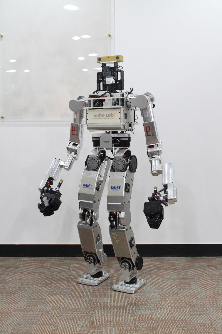 KAIST's HUBO Ready for DARPA's Robotics Challenge Trials
When walking on muddy or bumpy roads, the two arms of DRC-HUBO become extra legs, enabling stable and agile movements.
The Humanoid Robot Research Center (HUBO Lab, http://hubolab.kaist.ac.kr) at the Korea Advanced Institute of Science and Technology (KAIST) and Rainbow Co., a spin-off venture company of the university, unveiled a new model of HUBO that will be entered in an international robotics competition scheduled later this year.
The competition is hosted and sponsored by the US Defense Advanced Research Projects Agency (DARPA), which is called the DARPA Robotics Challenge (DRC). Kicked off in October 2012, the DRC’s goal is to spur the development of advanced robots that can assist humans in mitigating and recovering from future natural and man-made disasters.
KAIST’s humanoid robot, HUBO, was originally created by Jun-Ho Oh, a distinguished professor of the Department of Mechanical Engineering, in 2004. Since then, the robot has gone through technological advancements, with the latest version of HUBO II released in 2012. So far, 12 HUBOs have been exported for further studies in robotics to universities, research institutes, and private companies in the US, China, and Singapore.
In tandem with Rainbow Co. (www.rainbow-robot.com), Professor Oh and his research team recently developed DRC-HUBO, which will compete as Team DRC-HUBO led by Drexel University at the DRC trials to be held in December 2013. Team DRC-HUBO is consisted of KAIST and nine US institutions.
DRC-HUBO is designed to perform difficult but essential activities required when responding to disaster scenes. The robot will have to fulfill eight tasks assigned by the DRC at the upcoming event such as driving a utility vehicle, walking across rough terrain, climbing a ladder, and using hand tools.
Unlike the previous models of HUBO, DRC-HUBO boasts several distinctive, enhanced features. Chief among them is the way the robot interacts with the external environment. Without complex sensors installed throughout the body, DRC-HUBO can control each joint of the arms and legs in compliance with the dynamics dictated by the external environment.
For example, when DRC-HUBO is faced with a rock falling from above while climbing up a ladder, the robot’s arms and legs naturally give in to the force of external changes. Accordingly, as the robot dodges the rock, its body and joints smoothly sway to absorb shock so that the fingers can keep a tight grip on the ladder, and the feet are planted firmly on the rail of the ladder, not losing balance.
In addition, DRC-HUBO can switch from bipedal to quadrupedal walking and vice versa. This provides the robot with greater stability to walk on uneven terrain or to climb up a hill. The robot’s arms and legs are elongated to better meet the challenges demanded by the DRC competition. DRC-HUBO’s two arms swing back and forth to form legs when necessary, thereby walking freely backwards and forwards.
The robot has gotten stronger grip as well. The right hand has four fingers (with one triggering finger that operates independently from the other three fingers), and the left hand has three fingers. All three fingers on both hands are actuated synchronously for gripping. The fingers are sophisticated enough to steer the wheel of a vehicle or grab a ladder to climb up, and strong enough to hold 15 lbs in one hand.
“With a full 34 degrees of freedom (DOF), DRC-HUBO stands 4.7 ft tall and weighs 120 lbs. All in all, the robot has been improved and extensively refurbished from the past models of HUBOs to compete at the DRC Trials. It has better vision and coordination. The legs and arms have become stronger,” said Professor Oh.
“Although the robot is still a prototype, it has important capabilities that can be utilized in advancing humanoid robots in general. One example is the way its arms can be used as extra legs to support the robot’s body, offering more flexibility in providing aid to humans.”
2013.07.25 View 16028
KAIST's HUBO Ready for DARPA's Robotics Challenge Trials
When walking on muddy or bumpy roads, the two arms of DRC-HUBO become extra legs, enabling stable and agile movements.
The Humanoid Robot Research Center (HUBO Lab, http://hubolab.kaist.ac.kr) at the Korea Advanced Institute of Science and Technology (KAIST) and Rainbow Co., a spin-off venture company of the university, unveiled a new model of HUBO that will be entered in an international robotics competition scheduled later this year.
The competition is hosted and sponsored by the US Defense Advanced Research Projects Agency (DARPA), which is called the DARPA Robotics Challenge (DRC). Kicked off in October 2012, the DRC’s goal is to spur the development of advanced robots that can assist humans in mitigating and recovering from future natural and man-made disasters.
KAIST’s humanoid robot, HUBO, was originally created by Jun-Ho Oh, a distinguished professor of the Department of Mechanical Engineering, in 2004. Since then, the robot has gone through technological advancements, with the latest version of HUBO II released in 2012. So far, 12 HUBOs have been exported for further studies in robotics to universities, research institutes, and private companies in the US, China, and Singapore.
In tandem with Rainbow Co. (www.rainbow-robot.com), Professor Oh and his research team recently developed DRC-HUBO, which will compete as Team DRC-HUBO led by Drexel University at the DRC trials to be held in December 2013. Team DRC-HUBO is consisted of KAIST and nine US institutions.
DRC-HUBO is designed to perform difficult but essential activities required when responding to disaster scenes. The robot will have to fulfill eight tasks assigned by the DRC at the upcoming event such as driving a utility vehicle, walking across rough terrain, climbing a ladder, and using hand tools.
Unlike the previous models of HUBO, DRC-HUBO boasts several distinctive, enhanced features. Chief among them is the way the robot interacts with the external environment. Without complex sensors installed throughout the body, DRC-HUBO can control each joint of the arms and legs in compliance with the dynamics dictated by the external environment.
For example, when DRC-HUBO is faced with a rock falling from above while climbing up a ladder, the robot’s arms and legs naturally give in to the force of external changes. Accordingly, as the robot dodges the rock, its body and joints smoothly sway to absorb shock so that the fingers can keep a tight grip on the ladder, and the feet are planted firmly on the rail of the ladder, not losing balance.
In addition, DRC-HUBO can switch from bipedal to quadrupedal walking and vice versa. This provides the robot with greater stability to walk on uneven terrain or to climb up a hill. The robot’s arms and legs are elongated to better meet the challenges demanded by the DRC competition. DRC-HUBO’s two arms swing back and forth to form legs when necessary, thereby walking freely backwards and forwards.
The robot has gotten stronger grip as well. The right hand has four fingers (with one triggering finger that operates independently from the other three fingers), and the left hand has three fingers. All three fingers on both hands are actuated synchronously for gripping. The fingers are sophisticated enough to steer the wheel of a vehicle or grab a ladder to climb up, and strong enough to hold 15 lbs in one hand.
“With a full 34 degrees of freedom (DOF), DRC-HUBO stands 4.7 ft tall and weighs 120 lbs. All in all, the robot has been improved and extensively refurbished from the past models of HUBOs to compete at the DRC Trials. It has better vision and coordination. The legs and arms have become stronger,” said Professor Oh.
“Although the robot is still a prototype, it has important capabilities that can be utilized in advancing humanoid robots in general. One example is the way its arms can be used as extra legs to support the robot’s body, offering more flexibility in providing aid to humans.”
2013.07.25 View 16028 -
KAIST develops a low-power 60 GHz radio frequency chip for mobile devices
As the capacity of handheld devices increases to accommodate a greater number of functions, these devices have more memory, larger display screens, and the ability to play higher definition video files. If the users of mobile devices, including smartphones, tablet PCs, and notebooks, want to share or transfer data on one device with that of another device, a great deal of time and effort are needed.
As a possible method for the speedy transmission of large data, researchers are studying the adoption of gigabits per second (Gbps) wireless communications operating over the 60 gigahertz (GHz) frequency band. Some commercial approaches have been introduced for full-HD video streaming from a fixed source to a display by using the 60 GHz band. But mobile applications have not been developed yet because the 60 GHz radio frequency (RF) circuit consumes hundreds of milliwatts (mW) of DC power.
Professor Chul Soon Park from the Department of Electrical Engineering at the Korea Advanced Institute of Science and Technology (KAIST) and his research team recently developed a low-power version of the 60 GHz radio frequency integrated circuit (RFIC). Inside the circuit are an energy-efficient modulator performing amplification as well as modulation and a sensitivity-improved receiver employing a gain boosting demodulator.
The research team said that their RFIC draws as little as 67 mW of power in the 60 GHz frequency band, consuming 31mW to send and 36mW to receive large volumes of data. RFIC is also small enough to be mounted on smartphones or notebooks, requiring only one chip (its width, length, and height are about 1 mm) and one antenna (4x5x1 mm3) for sending and receiving data with an integrated switch.
Professor Park, Director of the Intelligent Radio Engineering Center at KAIST, gave an upbeat assessment of the potential of RFIC for future applications. What we have developed is a low-power 60-GHz RF chip with a transmission speed of 10.7 gigabits per second. In tests, we were able to stream uncompressed full-HD videos from a smartphone or notebook to a display without a cable connection (Youtube Link: http://www.youtube.com/watch?v=6PVSLBhMymc). Our chip can be installed on mobile devices or even on cameras so that the devices are virtually connected to other devices and able to exchange large data with each other."
2013.04.02 View 9752
-
A Substance with Amazingly Improved Efficiency of Capturing Carbon Dioxides Developed
From left to right: Prof.Ali Coskun, Prof. Cafer T. Yavuz and Prof. Yousung Jung
- Selectivity of CO2 increased by 300 times in comparison to nitrogen, published in Nature Communications-
KAIST EEWS graduate school’s joint research team led by Prof. Cafer T. Yavuz, Prof. Ali Coskun, and Prof. Yousung Jung has developed the world"s most efficient CO2 absorbent that has 300 times higher carbon dioxide selectivity in comparison to nitrogen.
Recently, the importance of CCS* technology, which is about capturing, storing and treating carbon dioxides, has begun to emerge world-widely as a practical alternative for the response to climate change.
* CCS : Carbon Capture and sequestration
Current carbon dioxide capturing technologies are wet capturing using liquid absorbent, dry capturing using solid absorbent and separation-membrane capturing using a thin membrane like a film.
For the places like power plant and forge, where the emission of carbon dioxides is huge, the main task is to maintain the capturing efficiency under extremely hot and humid conditions.
The previously studied dry absorbents, such as MOF or zeolite, had the disadvantages of instability in moist conditions and expensive cost for synthesis.
On the other hand, the research team"s newly discovered dry absorbent, named ‘Azo-COP’, can be synthesized without any expensive catalysts so the production cost is very low. It is also stable under hot and humid conditions.
COP is a structure consisting of simple organic molecules combined into porous polymer and is the first dry carbon dioxide capturing material developed by this research team.
The research team introduced an additional functional group called "Azo" to the substance, so that it can selectively capture carbon dioxides among the mixture of gas.
Azo-COP, which includes ‘Azo’ functional group, is manufactured easily by using common synthesis methods, and impurities are removed simply by using cheap solvents like water and acetone instead of expensive catalysts. As a result, the manufacturing cost has lowered drastically.
Especially, Azo-COP is combined with carbon dioxides by weak attraction force rather than chemical attraction so the recycling energy cost for the absorbent can be reduced innovatively, and it is expected to be used for capturing substances other than carbon dioxides in various areas as it is stable under extreme conditions even under 350 degrees Celsius.
This research is supported by Korea Carbon Capture&Sequestration R&D Center(Head: Sangdo Park) and KAIST EEWS planning group.
Prof. Cafer T. Yavuz and Prof. Ali Coskun said that “when Azo-COP is used for separation of CO2 and N2, the capturing efficiency has increased by hundred times.” He continued “This substance does not need any catalysts and has great chemical characteristics like water stability and structure stability so is expected to be used in various fields including carbon dioxides capturing”
Meanwhile, this research is published in ‘Nature’s stablemate ‘Nature Communications’ on 15th of Jan.
2013.02.24 View 14020
-
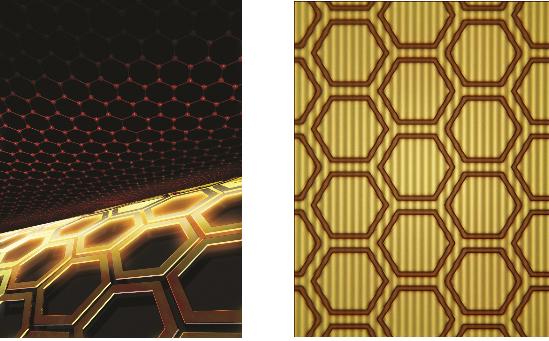 The control of light at the nano-level
Professor Min Bumki
Professor Min Bumki’s research team from the Department of Mechanical Engineering at KAIST have successfully gained control of the transmittance of light in optical devices using graphene* and artificial 2-dimensional metamaterials**.
* Graphene : a thin membrane composed of pure carbon, with atoms arranged in a regular hexagonal pattern
** Metamaterials : artificial materials engineered to have properties that may not be found in nature
The research results were published in the recent online edition (September 30th) of Nature Materials, a sister journal of the world renowned Nature journal, under the title ‘Terahertz waves with gate-controlled active graphene metamaterials’
Since the discovery of graphene in 2004 by Professors Novoselov and Geim from the University of Manchester (2010 Nobel Prize winners in Physics), it has been dubbed “the dream material” because of its outstanding physical properties.
Graphene has been especially praised for its ability to absorb approximately 2.3% of near infrared and visible rays due to its characteristic electron structure. This property allows graphene to be used as a transparent electrode, which is a vital electrical component used in touch screens and solar batteries. However, graphene’s optical transmittance was largely ignored by researchers due to its limited control using electrical methods and its small optical modulation in data transfer.
Professor Min’s team combined 0.34 nanometer-thick graphene with metamaterials to allow a more effective control of light transmittance and greater optical modulation. This graphene metamaterial can be integrated in to a thin and flexible macromolecule substrate which allows the control of transmittance using electric signals.
This research experimentally showed that graphene metamaterials can not only effective control optical transmittance, but can also be used in graphene optical memory devices using electrical hysteresis.
Professor Min said that “this research allows the effective control of light at the nanometer level” and that “this research will help in the development of microscopic optical modulators or memory disks”.
figure 1. The working drawing of graphene metamaterials
figure 2. Conceptual diagram (Left) and microscopic photo (right) of graphene metamaterials
2012.11.23 View 12031
The control of light at the nano-level
Professor Min Bumki
Professor Min Bumki’s research team from the Department of Mechanical Engineering at KAIST have successfully gained control of the transmittance of light in optical devices using graphene* and artificial 2-dimensional metamaterials**.
* Graphene : a thin membrane composed of pure carbon, with atoms arranged in a regular hexagonal pattern
** Metamaterials : artificial materials engineered to have properties that may not be found in nature
The research results were published in the recent online edition (September 30th) of Nature Materials, a sister journal of the world renowned Nature journal, under the title ‘Terahertz waves with gate-controlled active graphene metamaterials’
Since the discovery of graphene in 2004 by Professors Novoselov and Geim from the University of Manchester (2010 Nobel Prize winners in Physics), it has been dubbed “the dream material” because of its outstanding physical properties.
Graphene has been especially praised for its ability to absorb approximately 2.3% of near infrared and visible rays due to its characteristic electron structure. This property allows graphene to be used as a transparent electrode, which is a vital electrical component used in touch screens and solar batteries. However, graphene’s optical transmittance was largely ignored by researchers due to its limited control using electrical methods and its small optical modulation in data transfer.
Professor Min’s team combined 0.34 nanometer-thick graphene with metamaterials to allow a more effective control of light transmittance and greater optical modulation. This graphene metamaterial can be integrated in to a thin and flexible macromolecule substrate which allows the control of transmittance using electric signals.
This research experimentally showed that graphene metamaterials can not only effective control optical transmittance, but can also be used in graphene optical memory devices using electrical hysteresis.
Professor Min said that “this research allows the effective control of light at the nanometer level” and that “this research will help in the development of microscopic optical modulators or memory disks”.
figure 1. The working drawing of graphene metamaterials
figure 2. Conceptual diagram (Left) and microscopic photo (right) of graphene metamaterials
2012.11.23 View 12031 -
Jellyfish removal robot developed
Professor Myung Hyun’s research team from the Department of Civil and Environmental Engineering at KAIST has developed a jellyfish removal robot named ‘JEROS’ (JEROS: Jellyfish Elimination RObotic Swarm).
With jellyfish attacks around the south-west coast of Korea becoming a serious problem, causing deaths and operational losses (around 3 billion won a year), Professor Myung’s team started the development of this unmanned automatic jellyfish removal system 3 years ago.
JEROS floats on the surface of the water using two long cylindrical bodies. Motors are attached to the bodies such that the robot can move back and forth as well as rotate on water. A camera and GPS system allows the JEROS to detect jellyfish swarm as well as plan and calculate its work path relative to its position.
The jellyfish are removed by a submerged net that sucks them up using the velocity created by the unmanned sailing. Once caught, the jellyfish are pulverized using a special propeller.
JEROS is estimated to be 3 times more economical than manual removal. Upon experimentation, it showed a removal rate of 400kg per hour at 6 knots. To reach similar effectiveness as manual net removal, which removes up to 1 ton per hour, the research team designed the robot such that 3 or more individual robots could be grouped together and controlled as one.
The research team has finished conducting removal tests in Gunsan and Masan and plan to commercialize the robot next April after improving the removal technology. JEROS technology can also be used for a wide range of purposes such as patrolling and guarding, preventing oil spills or removing floating waste. This research was funded by the Ministry of Education, Science and Technology since 2010.
2012.08.29 View 13938
-
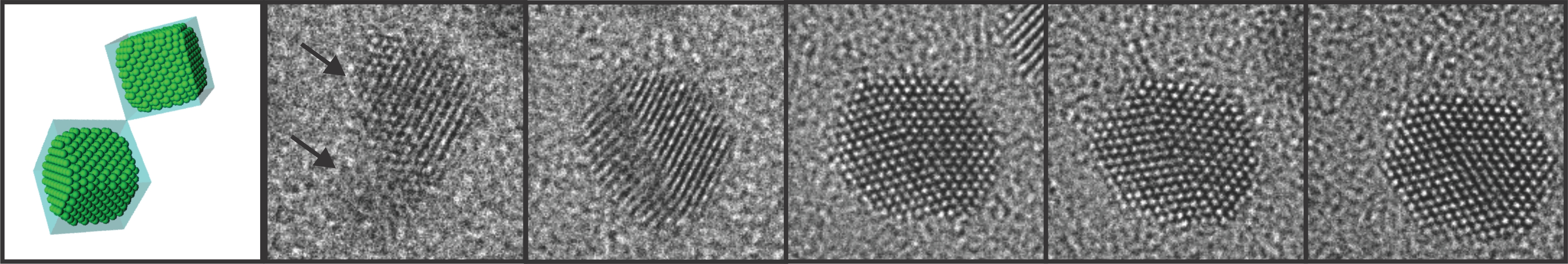 High-resolution Atomic Imaging of Specimens in Liquid Observed by Transmission Electron Microscopes Using Graphene Liquid Cells
Looking into specimens in liquid at the atomic level to understand nanoscale processes so far regarded as impossible to witnessThe Korea Advanced Institute of Science and Technology (KAIST) announced that a research team from the Department of Materials Science and Engineering has developed a technology that enables scientists and engineers to observe processes occurring in liquid media on the smallest possible scale which is less than a nanometer.
Professor Jeong Yong Lee and Researcher Jong Min Yuk, in collaboration with Professors Paul Alivisatos’s and Alex Zettl’s groups at the University of California, Berkeley, succeeded in making a graphene liquid cell or capsule, confining an ultra-thin liquid film between layers of graphene, for real-time and in situ imagining of nanoscale processes in fluids with atomic-level resolution by a transmission electron microscope (TEM). Their research was published in the April 6, 2012 issue of Science. (http://www.sciencemag.org/content/336/6077/61.abstract)
The graphene liquid cell (GLC) is composed of two sheets of graphene sandwiched to create a sealed chamber where a platinum growth solution is encapsulated in the form of a thin slice. Each graphene layer has a thickness of one carbon atom, the thinnest membrane that has ever been used to fabricate a liquid cell required for TEM.
The research team peered inside the GLC to observe the growth and dynamics of platinum nanocrystals in solution as they coalesced into a larger size, during which the graphene membrane with the encapsulated liquid remained intact. The researchers from KAIST and the UC Berkeley identified important features in the ongoing process of the nanocrystals’ coalescence and their expansion through coalescence to form certain shapes by imaging the phenomena with atomic-level resolution.
Professor Lee said,
“It has now become possible for scientists to observe what is happening in liquids on an atomic level under transmission electron microscopes.”
Researcher Yuk, one of the first authors of the paper, explained his research work.
“This research will promote other fields of study related to materials in a fluid stage including physical, chemical, and biological phenomena at the atomic level and promises numerous applications in the future. Pending further studies on liquid microscopy, the full application of a graphene-liquid-cell (GLC) TEM to biological samples is yet to be confirmed. Nonetheless, the GLC is the most effective technique developed today to sustain the natural state of fluid samples or species suspended in the liquid for a TEM imaging.”
The transmission electron microscope (TEM), first introduced in the 1930s, produces images at a significantly higher resolution than light microscopes, allowing users to examine the smallest level of physical, chemical, and biological phenomena. Observations by TEM with atomic resolution, however, have been limited to solid and/or frozen samples, and thus it has previously been impossible to study the real time fluid dynamics of liquid phases.
TEM imaging is performed in a high vacuum chamber in which a thin slice of the imaged sample is situated, and an electron beam passes through the slice to create an image. In this process, a liquid medium, unlike solid or frozen samples, evaporates, making it difficult to observe under TEM.
Attempts to produce a liquid capsule have thus far been made with electron-transparent membranes of such materials as silicon nitride or silicon oxide; such liquid capsules are relatively thick (tens to one hundred nanometers), however, resulting in poor electron transmittance with a reduced resolution of only a few nanometers. Silicon nitride is 25 nanometers thick, whereas graphene is only 0.34 nanometers.
Graphene, most commonly found in bulk graphite, is the thinnest material made out of carbon atoms. It has unique properties such as mechanical tensile strength, high flexibility, impermeability to small molecules, and high electrical conductivity. Graphene is an excellent material to hold micro- and nanoscopic objects for observation in a transmission electron microscope by minimizing scattering of the electron beam that irradiates a liquid sample while reducing charging and heating effects.
###
Figure 1. Schematic illustration of graphene liquid cells. Sandwiched two sheets of graphene encapsulate a platinum growth solution.
Figure 2. In-situ TEM observation of nanocrystal growth and shape evolution. TEM images of platinum nanocrystal coalescence and their faceting in the growth solution.
2012.04.23 View 13387
High-resolution Atomic Imaging of Specimens in Liquid Observed by Transmission Electron Microscopes Using Graphene Liquid Cells
Looking into specimens in liquid at the atomic level to understand nanoscale processes so far regarded as impossible to witnessThe Korea Advanced Institute of Science and Technology (KAIST) announced that a research team from the Department of Materials Science and Engineering has developed a technology that enables scientists and engineers to observe processes occurring in liquid media on the smallest possible scale which is less than a nanometer.
Professor Jeong Yong Lee and Researcher Jong Min Yuk, in collaboration with Professors Paul Alivisatos’s and Alex Zettl’s groups at the University of California, Berkeley, succeeded in making a graphene liquid cell or capsule, confining an ultra-thin liquid film between layers of graphene, for real-time and in situ imagining of nanoscale processes in fluids with atomic-level resolution by a transmission electron microscope (TEM). Their research was published in the April 6, 2012 issue of Science. (http://www.sciencemag.org/content/336/6077/61.abstract)
The graphene liquid cell (GLC) is composed of two sheets of graphene sandwiched to create a sealed chamber where a platinum growth solution is encapsulated in the form of a thin slice. Each graphene layer has a thickness of one carbon atom, the thinnest membrane that has ever been used to fabricate a liquid cell required for TEM.
The research team peered inside the GLC to observe the growth and dynamics of platinum nanocrystals in solution as they coalesced into a larger size, during which the graphene membrane with the encapsulated liquid remained intact. The researchers from KAIST and the UC Berkeley identified important features in the ongoing process of the nanocrystals’ coalescence and their expansion through coalescence to form certain shapes by imaging the phenomena with atomic-level resolution.
Professor Lee said,
“It has now become possible for scientists to observe what is happening in liquids on an atomic level under transmission electron microscopes.”
Researcher Yuk, one of the first authors of the paper, explained his research work.
“This research will promote other fields of study related to materials in a fluid stage including physical, chemical, and biological phenomena at the atomic level and promises numerous applications in the future. Pending further studies on liquid microscopy, the full application of a graphene-liquid-cell (GLC) TEM to biological samples is yet to be confirmed. Nonetheless, the GLC is the most effective technique developed today to sustain the natural state of fluid samples or species suspended in the liquid for a TEM imaging.”
The transmission electron microscope (TEM), first introduced in the 1930s, produces images at a significantly higher resolution than light microscopes, allowing users to examine the smallest level of physical, chemical, and biological phenomena. Observations by TEM with atomic resolution, however, have been limited to solid and/or frozen samples, and thus it has previously been impossible to study the real time fluid dynamics of liquid phases.
TEM imaging is performed in a high vacuum chamber in which a thin slice of the imaged sample is situated, and an electron beam passes through the slice to create an image. In this process, a liquid medium, unlike solid or frozen samples, evaporates, making it difficult to observe under TEM.
Attempts to produce a liquid capsule have thus far been made with electron-transparent membranes of such materials as silicon nitride or silicon oxide; such liquid capsules are relatively thick (tens to one hundred nanometers), however, resulting in poor electron transmittance with a reduced resolution of only a few nanometers. Silicon nitride is 25 nanometers thick, whereas graphene is only 0.34 nanometers.
Graphene, most commonly found in bulk graphite, is the thinnest material made out of carbon atoms. It has unique properties such as mechanical tensile strength, high flexibility, impermeability to small molecules, and high electrical conductivity. Graphene is an excellent material to hold micro- and nanoscopic objects for observation in a transmission electron microscope by minimizing scattering of the electron beam that irradiates a liquid sample while reducing charging and heating effects.
###
Figure 1. Schematic illustration of graphene liquid cells. Sandwiched two sheets of graphene encapsulate a platinum growth solution.
Figure 2. In-situ TEM observation of nanocrystal growth and shape evolution. TEM images of platinum nanocrystal coalescence and their faceting in the growth solution.
2012.04.23 View 13387 -
Paving the Way to Next Generation Display
A new type of LCD that does not require polymer orientation films has been developed by researchers within the country. This technology will enable the creation of thiner and higher definition display.
Prof. Hee Tae Jung form KAIST’s biochemical engineering department led the research and Hyun Soo Jung, Hwan Jin Jeon doctoral students (1st co-authors), Doctor Yun Ho Kim from Korea Chemistry Research Center, and Prof. Shin Woong Kang from Jeon Buk University ( co-author) have participated in this research. This research has been funded by the WCU program and middle-grade researcher support program. The results of the research has been published as the online update of ‘‘Nature Asia Materials(NPG Asia Materials)” which is a sister magazine of the world renowned academic magazine ‘Nature’.
The flat display industry is the core industry leading the 21st century’s IT industry. The LCD is the main area of research. Korea is the leader of this industry, holding more than 50% of the world market. Many technologies are combined to make the electro-optic devices of the LCD function. The most important technology, which determines the indicating element’s quality and function is the technology to align the liquid crystals in one direction.
Currently, all LCD products are created by mechanically cutting into the surface of the polymer film and orienting the liquid crystal material along these cuts. However, the creation of polymer orientation films cost much time and money, and the high temperature processes necessary to stabilize the polymers does not allow for the free selection of circuit boards, and thus does not allow for the use in flexible display.
Prof. Hee Tae Jung devised a method to orient liquid display without the use of a polymer film using ITOs. Prof. Jung’s base technology has been tested on ITOs to maintain the necessary transparency and conductivity after forming a pattern with high decomposition rates and slenderness ratios.
The technology developed by the research team can horizontally or vertically align the transparent conductors without the use of polymer orientation films. Thus, the manufacturing processes have become much shortened and the LCDs can be made in much thinner from a few micrometers to a few centimeters. Also, it has a lower functioning voltage and faster response speed, showing the prospects of a high definition ultra-fast screen display development. Furthermore, this technology can be used for any type of board, and can be adjusted to a nanometer scale. This enables for its use in LCD based flexible or multi-domain modes.
Also, the transparent conductor patterning technology devised by the research team can be used not only for displays, but also for touch panels with highly increased sensitivity.
Prof. Jung said, “It was a long desire of the industry and academia to find a way to replace the polymer orientation film. This new technology does not need any polymer orientation films, and we can still use the original boards used for LCDs. This mean a lot to the industry. Also, this technology will increase the sensitivity of the touch panels for tablet PCs and smart phones. It can be used in many areas of future electronics base technology.”
2012.04.04 View 12385
-
Inexpensive Separation Method of Graphene Developed
The problem with commercializing graphene that is synthesized onto metals over a wide area is that it can not be separated from the metal. However, a groundbreaking separation technology which is both cheap and environment friendly has been developed.
Prof. Taek soo Kim and Prof. Byung Jin Cho"s research teams have conducted this research under the support of the Global Frontier program and Researcher Support Program initiated by The Ministry of Education and Science and Korea Research Foundation. The research results have been posted on the online news flash of Nano Letters on februrary 29th. (Thesis title: Direct Measurement of Adhesion Energy of Monolayer Graphene As-Grown on Copper and Its Application to Renewable Transfer Process)
The research has generated exact results on the interfacial adhesive energy of graphene and its surface material for the first time. Through this, the catalyst metal are no longer to be used just once, but will be used for an infinite number of times, thereby being ecofriendly and efficient.
Wide area graphine synthesized onto the catalyst meatal are used in various ways such as for display and for solar cells. There has been much research going on in this field. However, in order to use this wide area graphene, the graphene must be removed from the catalyst metal without damage.
Until now, the metal had been melted away through the use of chemical substances in order to separate the graphene. However, this method has been very problematic. The metal can not be reused, the costs are very high, much harmful wastes were created in the process of melting the metals, and the process was very complicated.
The research teams of Professors Taek Su Kim and Byung Jin Cho measured the interfacial adhesive energy of the synthesized graphene and learned that it could be easily removed.
Also, the mechanically removed graphene was successfully used in creating molecular electronic devices directly. This has thus innovatively shortened the graphene manufacturing process. Also, it has been confirmed that the metalic board can be reused multiple times after the graphene is removed. A new, ecofriendly and cost friendly method of graphene manufacturing has been paved.
Through this discovery, it is expected that graphene will become easier to manufacture and that the period til the commercialization date of graphene will therefore be greatly reduced
Prof. Cho stated " This reserach has much academical meaning significance in that it has successfully defined the surfacial adhesive energy between the graphene and its catalyst material and it should receive much attention in that it solved the largest technical problem involved in the production of graphene.
2012.04.04 View 16918
-
Closer to the Dream: Graphene
A technique that allows easy and larger observation area of graphene’s crystal face was developed by Korean Research Team.
The research team, led by Professor Jeong Hui Tae (KAIST), consists of Doctorate candidate Kim Dae Woo, Dr. Kim Yoon Ho (primary author), Doctorate candidate Jeong Hyun Soo. The research is supported by WCU (World Class Research University) Development Plan, Mid-Aged Researcher Support Business and was published in the online edition of Nature Nanotechnology.
(Dissertation: Direct visualization of large0area graphene domains and boundaries by optical birefringency)
Professor Jeong’s team used the optical property of the liquid display used in LCD to visualize the size and shape of the single crystals along a flat surface. The visualization of the single crystal allowed the measurement of a near theoretical value of electrical conductivity of graphene.
Graphene has great electrical conductivity, transparent, mechanically stable, flexible, and is therefore regarded as the next generation electrical material. However the polycrystalinity of graphene meant that the actual electrical, mechanical properties were lower than the theoretical values. The reason was thought to be because of the size of the crystal faces and boundary structures.
Therefore, in order to create graphene that has good properties, observing the domain and boundary of graphene crystal faces is essential.
The new technique developed by the research team is another step towards commercializing transparent electrodes, flexible display, and electric materials like solar cells.
2012.01.31 View 12605
-
Quantum Mechanical Calculation Theory Developed
An Electron Density Functional Calculation Theory, based on the widely used quantum mechanical principles and yet accurate and with shortened calculation period, was developed by Korean research team.
*Electron Density Functional Calculation Theory: Theory that proves that it is possible to calculate energy and properties with only simple wave equations and electron densities.
The research was conducted by Professor Jeong Yoo Sung (Graduate School of EEWS) and Professor William Goddard with support from WCU Foster Project initiated by Ministry of Education, Science and Technology and Korea Research Foundation. The result was published in the Proceedings of the National Academy of Sciences Journal.
The research team corrected the error when performing quantum calculations that arises from the length of calculation time and incorrect assumptions and developed a theory and algorithm that is more accurate and faster. The use of wave equations in quantum mechanical calculations results in high accuracy but there is a rapid increase in calculation time and is therefore difficult to implement in large molecules with hundreds, or thousands of atoms. By implementing a low electron density variable with relatively less calculation work, the size of calculable molecule increases but the accuracy decreases.
The team focused on the interaction between electrons with different spins to improve upon the speed of calculation in the conventional accurate calculation. The team used the fact that the interaction between electrons with different spins increases as it comes closer together in accordance with the Pauli’s Exclusion Principle.
In addition the interaction between electrons are local and therefore can ignore the interactions between far away electrons and still get the total energy value. The team also took advantage of this fact and developed the algorithm that decreased calculation time hundredth fold.
Professor Jeong commented that, “So far most of the domestic achievements were made by focusing on integrative researches by calculation science and material design communities but these involved short time frames. In areas that required lengthy time frames like fundamentals and software development, there was no competitive advantage. However this research is significant in that a superior solution was developed domestically”.
2012.01.31 View 13548
-
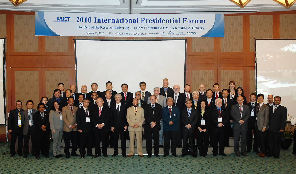 2010 International Presidential Forum was held successfully.
On October 11th, the 2010 International Presidential Forum on “The Role of the Research University in an S&T Dominated Era: Expectation & Delivery” was held successfully at the Westin Chosun Hotel in Seoul. The third International Presidential Forum to be held, participants of the 2010 Presidential Forum engaged in an in-depth discussion about the direction that research universities should take in the 21st Century.
On its opening, President Nam Pyo Suh delivered a congratulatory message saying, “This forum is a meaningful gathering where research universities will suggest role models and find ways research universities can contribute to the progress of mankind in this century.”
Following, Lee Ki Jun, CEO of the Korean Federation of Science and Technology Societies said, “The common goal of the world’s research universities is to solve the problems mankind is facing together. I believe that the discussion we will hold today at the forum will point to the future direction of research universities.”
“To produce next generation engineers meeting global standards, exchange and dual degree programs between universities must be strengthened,” said Lars Pallesen, President of the Technical University of Denmark. “Research universities must support the exchange between students beyond cultural and national borders to adapt to the global market.”
Ichiro Okura, Vice President of Tokyo Institute of Technology, presented on the “Asian Science and Technology Pioneering Institutes of Research and Education, ASPIRE.” ASPIRE is a community created by the coalition between science and technology universities in the Far East. Its purpose is to contribute to sustainable global growth by educating high-quality human resources and lead Asia’s technology innovation based on science and technology development.
“For research universities to solve today’s global issues, universities must create new ideas by performing fundamental studies and developing innovative technology. The financial resources of universities must be focused with choices based on results,” remarked President Suh.
Zaini Ujang, Vice-President of the Universiti Teknologi Malaysia stated that “the Malaysian government is planning on converting from a ‘labor-intensive economy’ to an ‘innovative leading economy’ with the goal of joining the advanced countries by 2020. In today’s science and technology era where innovative technology is necessary, research universities have an important role of developing the knowledge environmental system to lead the world economy.” Vice-President Ujang then explained what strategies Malaysian research universities devised in the innovative leading economy era to create research universities that bring creativity and innovation.
Tod A. Laursen, President of KUSTAR, said that “KUSTAR has a leading role in bringing science and technology and manpower necessary in converting the oil-centered economy of UAE to a knowledge-based economy. KUSTAR will continuously strengthen international cooperation to become not only the best engineering university in the Arab region but in the world.”
At this year’s forum, thirty international presidents and vice presidents from 24 universities in 15 countries including Georgia Tech, Technical University of Denmark, Technion-Israel Institute of Technology, University of Queensland, Tokyo University, Nanyang Technological University, University Teknologi Malaysia and Hong Kong Institute of Science and Technology along with forty national figures such as the presidents of Hanyang University and Handong Global University, governmental bureaucrats and representatives from national business and institutions participated.
2010.10.20 View 19629
2010 International Presidential Forum was held successfully.
On October 11th, the 2010 International Presidential Forum on “The Role of the Research University in an S&T Dominated Era: Expectation & Delivery” was held successfully at the Westin Chosun Hotel in Seoul. The third International Presidential Forum to be held, participants of the 2010 Presidential Forum engaged in an in-depth discussion about the direction that research universities should take in the 21st Century.
On its opening, President Nam Pyo Suh delivered a congratulatory message saying, “This forum is a meaningful gathering where research universities will suggest role models and find ways research universities can contribute to the progress of mankind in this century.”
Following, Lee Ki Jun, CEO of the Korean Federation of Science and Technology Societies said, “The common goal of the world’s research universities is to solve the problems mankind is facing together. I believe that the discussion we will hold today at the forum will point to the future direction of research universities.”
“To produce next generation engineers meeting global standards, exchange and dual degree programs between universities must be strengthened,” said Lars Pallesen, President of the Technical University of Denmark. “Research universities must support the exchange between students beyond cultural and national borders to adapt to the global market.”
Ichiro Okura, Vice President of Tokyo Institute of Technology, presented on the “Asian Science and Technology Pioneering Institutes of Research and Education, ASPIRE.” ASPIRE is a community created by the coalition between science and technology universities in the Far East. Its purpose is to contribute to sustainable global growth by educating high-quality human resources and lead Asia’s technology innovation based on science and technology development.
“For research universities to solve today’s global issues, universities must create new ideas by performing fundamental studies and developing innovative technology. The financial resources of universities must be focused with choices based on results,” remarked President Suh.
Zaini Ujang, Vice-President of the Universiti Teknologi Malaysia stated that “the Malaysian government is planning on converting from a ‘labor-intensive economy’ to an ‘innovative leading economy’ with the goal of joining the advanced countries by 2020. In today’s science and technology era where innovative technology is necessary, research universities have an important role of developing the knowledge environmental system to lead the world economy.” Vice-President Ujang then explained what strategies Malaysian research universities devised in the innovative leading economy era to create research universities that bring creativity and innovation.
Tod A. Laursen, President of KUSTAR, said that “KUSTAR has a leading role in bringing science and technology and manpower necessary in converting the oil-centered economy of UAE to a knowledge-based economy. KUSTAR will continuously strengthen international cooperation to become not only the best engineering university in the Arab region but in the world.”
At this year’s forum, thirty international presidents and vice presidents from 24 universities in 15 countries including Georgia Tech, Technical University of Denmark, Technion-Israel Institute of Technology, University of Queensland, Tokyo University, Nanyang Technological University, University Teknologi Malaysia and Hong Kong Institute of Science and Technology along with forty national figures such as the presidents of Hanyang University and Handong Global University, governmental bureaucrats and representatives from national business and institutions participated.
2010.10.20 View 19629