research
-
 Image Analysis to Automatically Quantify Gender Bias in Movies
Many commercial films worldwide continue to express womanhood in a stereotypical manner, a recent study using image analysis showed. A KAIST research team developed a novel image analysis method for automatically quantifying the degree of gender bias in films.
The ‘Bechdel Test’ has been the most representative and general method of evaluating gender bias in films. This test indicates the degree of gender bias in a film by measuring how active the presence of women is in a film. A film passes the Bechdel Test if the film (1) has at least two female characters, (2) who talk to each other, and (3) their conversation is not related to the male characters.
However, the Bechdel Test has fundamental limitations regarding the accuracy and practicality of the evaluation. Firstly, the Bechdel Test requires considerable human resources, as it is performed subjectively by a person. More importantly, the Bechdel Test analyzes only a single aspect of the film, the dialogues between characters in the script, and provides only a dichotomous result of passing the test, neglecting the fact that a film is a visual art form reflecting multi-layered and complicated gender bias phenomena. It is also difficult to fully represent today’s various discourse on gender bias, which is much more diverse than in 1985 when the Bechdel Test was first presented.
Inspired by these limitations, a KAIST research team led by Professor Byungjoo Lee from the Graduate School of Culture Technology proposed an advanced system that uses computer vision technology to automatically analyzes the visual information of each frame of the film. This allows the system to more accurately and practically evaluate the degree to which female and male characters are discriminatingly depicted in a film in quantitative terms, and further enables the revealing of gender bias that conventional analysis methods could not yet detect.
Professor Lee and his researchers Ji Yoon Jang and Sangyoon Lee analyzed 40 films from Hollywood and South Korea released between 2017 and 2018. They downsampled the films from 24 to 3 frames per second, and used Microsoft’s Face API facial recognition technology and object detection technology YOLO9000 to verify the details of the characters and their surrounding objects in the scenes.
Using the new system, the team computed eight quantitative indices that describe the representation of a particular gender in the films. They are: emotional diversity, spatial staticity, spatial occupancy, temporal occupancy, mean age, intellectual image, emphasis on appearance, and type and frequency of surrounding objects.
Figure 1. System Diagram
Figure 2. 40 Hollywood and Korean Films Analyzed in the Study
According to the emotional diversity index, the depicted women were found to be more prone to expressing passive emotions, such as sadness, fear, and surprise. In contrast, male characters in the same films were more likely to demonstrate active emotions, such as anger and hatred.
Figure 3. Difference in Emotional Diversity between Female and Male Characters
The type and frequency of surrounding objects index revealed that female characters and automobiles were tracked together only 55.7 % as much as that of male characters, while they were more likely to appear with furniture and in a household, with 123.9% probability.
In cases of temporal occupancy and mean age, female characters appeared less frequently in films than males at the rate of 56%, and were on average younger in 79.1% of the cases. These two indices were especially conspicuous in Korean films.
Professor Lee said, “Our research confirmed that many commercial films depict women from a stereotypical perspective. I hope this result promotes public awareness of the importance of taking prudence when filmmakers create characters in films.”
This study was supported by KAIST College of Liberal Arts and Convergence Science as part of the Venture Research Program for Master’s and PhD Students, and will be presented at the 22nd ACM Conference on Computer-Supported Cooperative Work and Social Computing (CSCW) on November 11 to be held in Austin, Texas.
Publication:
Ji Yoon Jang, Sangyoon Lee, and Byungjoo Lee. 2019. Quantification of Gender Representation Bias in Commercial Films based on Image Analysis. In Proceedings of the 22nd ACM Conference on Computer-Supported Cooperative Work and Social Computing (CSCW). ACM, New York, NY, USA, Article 198, 29 pages. https://doi.org/10.1145/3359300
Link to download the full-text paper:
https://files.cargocollective.com/611692/cscw198-jangA--1-.pdf
Profile: Prof. Byungjoo Lee, MD, PhD
byungjoo.lee@kaist.ac.kr
http://kiml.org/
Assistant Professor
Graduate School of Culture Technology (CT)
Korea Advanced Institute of Science and Technology (KAIST)
https://www.kaist.ac.kr Daejeon 34141, Korea
Profile: Ji Yoon Jang, M.S.
yoone3422@kaist.ac.kr
Interactive Media Lab
Graduate School of Culture Technology (CT)
Korea Advanced Institute of Science and Technology (KAIST)
https://www.kaist.ac.kr Daejeon 34141, Korea
Profile: Sangyoon Lee, M.S. Candidate
sl2820@kaist.ac.kr
Interactive Media Lab
Graduate School of Culture Technology (CT)
Korea Advanced Institute of Science and Technology (KAIST)
https://www.kaist.ac.kr Daejeon 34141, Korea
(END)
2019.10.17 View 27592
Image Analysis to Automatically Quantify Gender Bias in Movies
Many commercial films worldwide continue to express womanhood in a stereotypical manner, a recent study using image analysis showed. A KAIST research team developed a novel image analysis method for automatically quantifying the degree of gender bias in films.
The ‘Bechdel Test’ has been the most representative and general method of evaluating gender bias in films. This test indicates the degree of gender bias in a film by measuring how active the presence of women is in a film. A film passes the Bechdel Test if the film (1) has at least two female characters, (2) who talk to each other, and (3) their conversation is not related to the male characters.
However, the Bechdel Test has fundamental limitations regarding the accuracy and practicality of the evaluation. Firstly, the Bechdel Test requires considerable human resources, as it is performed subjectively by a person. More importantly, the Bechdel Test analyzes only a single aspect of the film, the dialogues between characters in the script, and provides only a dichotomous result of passing the test, neglecting the fact that a film is a visual art form reflecting multi-layered and complicated gender bias phenomena. It is also difficult to fully represent today’s various discourse on gender bias, which is much more diverse than in 1985 when the Bechdel Test was first presented.
Inspired by these limitations, a KAIST research team led by Professor Byungjoo Lee from the Graduate School of Culture Technology proposed an advanced system that uses computer vision technology to automatically analyzes the visual information of each frame of the film. This allows the system to more accurately and practically evaluate the degree to which female and male characters are discriminatingly depicted in a film in quantitative terms, and further enables the revealing of gender bias that conventional analysis methods could not yet detect.
Professor Lee and his researchers Ji Yoon Jang and Sangyoon Lee analyzed 40 films from Hollywood and South Korea released between 2017 and 2018. They downsampled the films from 24 to 3 frames per second, and used Microsoft’s Face API facial recognition technology and object detection technology YOLO9000 to verify the details of the characters and their surrounding objects in the scenes.
Using the new system, the team computed eight quantitative indices that describe the representation of a particular gender in the films. They are: emotional diversity, spatial staticity, spatial occupancy, temporal occupancy, mean age, intellectual image, emphasis on appearance, and type and frequency of surrounding objects.
Figure 1. System Diagram
Figure 2. 40 Hollywood and Korean Films Analyzed in the Study
According to the emotional diversity index, the depicted women were found to be more prone to expressing passive emotions, such as sadness, fear, and surprise. In contrast, male characters in the same films were more likely to demonstrate active emotions, such as anger and hatred.
Figure 3. Difference in Emotional Diversity between Female and Male Characters
The type and frequency of surrounding objects index revealed that female characters and automobiles were tracked together only 55.7 % as much as that of male characters, while they were more likely to appear with furniture and in a household, with 123.9% probability.
In cases of temporal occupancy and mean age, female characters appeared less frequently in films than males at the rate of 56%, and were on average younger in 79.1% of the cases. These two indices were especially conspicuous in Korean films.
Professor Lee said, “Our research confirmed that many commercial films depict women from a stereotypical perspective. I hope this result promotes public awareness of the importance of taking prudence when filmmakers create characters in films.”
This study was supported by KAIST College of Liberal Arts and Convergence Science as part of the Venture Research Program for Master’s and PhD Students, and will be presented at the 22nd ACM Conference on Computer-Supported Cooperative Work and Social Computing (CSCW) on November 11 to be held in Austin, Texas.
Publication:
Ji Yoon Jang, Sangyoon Lee, and Byungjoo Lee. 2019. Quantification of Gender Representation Bias in Commercial Films based on Image Analysis. In Proceedings of the 22nd ACM Conference on Computer-Supported Cooperative Work and Social Computing (CSCW). ACM, New York, NY, USA, Article 198, 29 pages. https://doi.org/10.1145/3359300
Link to download the full-text paper:
https://files.cargocollective.com/611692/cscw198-jangA--1-.pdf
Profile: Prof. Byungjoo Lee, MD, PhD
byungjoo.lee@kaist.ac.kr
http://kiml.org/
Assistant Professor
Graduate School of Culture Technology (CT)
Korea Advanced Institute of Science and Technology (KAIST)
https://www.kaist.ac.kr Daejeon 34141, Korea
Profile: Ji Yoon Jang, M.S.
yoone3422@kaist.ac.kr
Interactive Media Lab
Graduate School of Culture Technology (CT)
Korea Advanced Institute of Science and Technology (KAIST)
https://www.kaist.ac.kr Daejeon 34141, Korea
Profile: Sangyoon Lee, M.S. Candidate
sl2820@kaist.ac.kr
Interactive Media Lab
Graduate School of Culture Technology (CT)
Korea Advanced Institute of Science and Technology (KAIST)
https://www.kaist.ac.kr Daejeon 34141, Korea
(END)
2019.10.17 View 27592 -
 A Mathematical Model Reveals Long-Distance Cell Communication Mechanism
How can tens of thousands of people in a large football stadium all clap together with the same beat even though they can only hear the people near them clapping?
A combination of a partial differential equation and a synthetic circuit in microbes answers this question. An interdisciplinary collaborative team of Professor Jae Kyoung Kim at KAIST, Professor Krešimir Josić at the University of Houston, and Professor Matt Bennett at Rice University has identified how a large community can communicate with each other almost simultaneously even with very short distance signaling. The research was reported at Nature Chemical Biology.
Cells often communicate using signaling molecules, which can travel only a short distance. Nevertheless, the cells can also communicate over large distances to spur collective action. The team revealed a cell communication mechanism that quickly forms a network of local interactions to spur collective action, even in large communities.
The research team used an engineered transcriptional circuit of combined positive and negative feedback loops in E. coli, which can periodically release two types of signaling molecules: activator and repressor. As the signaling molecules travel over a short distance, cells can only talk to their nearest neighbors. However, cell communities synchronize oscillatory gene expression in spatially extended systems as long as the transcriptional circuit contains a positive feedback loop for the activator.
Professor Kim said that analyzing and understanding such high-dimensional dynamics was extremely difficult. He explained, “That’s why we used high-dimensional partial differential equation to describe the system based on the interactions among various types of molecules.” Surprisingly, the mathematical model accurately simulates the synthesis of the signaling molecules in the cell and their spatial diffusion throughout the chamber and their effect on neighboring cells.
The team simplified the high-dimensional system into a one-dimensional orbit, noting that the system repeats periodically. This allowed them to discover that cells can make one voice when they lowered their own voice and listened to the others. “It turns out the positive feedback loop reduces the distance between moving points and finally makes them move all together. That’s why you clap louder when you hear applause from nearby neighbors and everyone eventually claps together at almost the same time,” said Professor Kim.
Professor Kim added, “Math is a powerful as it simplifies complex thing so that we can find an essential underlying property. This finding would not have been possible without the simplification of complex systems using mathematics."
The National Institutes of Health, the National Science Foundation, the Robert A. Welch Foundation, the Hamill Foundation, the National Research Foundation of Korea, and the T.J. Park Science Fellowship of POSCO supported the research.
(Figure: Complex molecular interactions among microbial consortia is simplified as interactions among points on a limit cycle (right).)
2019.10.15 View 29472
A Mathematical Model Reveals Long-Distance Cell Communication Mechanism
How can tens of thousands of people in a large football stadium all clap together with the same beat even though they can only hear the people near them clapping?
A combination of a partial differential equation and a synthetic circuit in microbes answers this question. An interdisciplinary collaborative team of Professor Jae Kyoung Kim at KAIST, Professor Krešimir Josić at the University of Houston, and Professor Matt Bennett at Rice University has identified how a large community can communicate with each other almost simultaneously even with very short distance signaling. The research was reported at Nature Chemical Biology.
Cells often communicate using signaling molecules, which can travel only a short distance. Nevertheless, the cells can also communicate over large distances to spur collective action. The team revealed a cell communication mechanism that quickly forms a network of local interactions to spur collective action, even in large communities.
The research team used an engineered transcriptional circuit of combined positive and negative feedback loops in E. coli, which can periodically release two types of signaling molecules: activator and repressor. As the signaling molecules travel over a short distance, cells can only talk to their nearest neighbors. However, cell communities synchronize oscillatory gene expression in spatially extended systems as long as the transcriptional circuit contains a positive feedback loop for the activator.
Professor Kim said that analyzing and understanding such high-dimensional dynamics was extremely difficult. He explained, “That’s why we used high-dimensional partial differential equation to describe the system based on the interactions among various types of molecules.” Surprisingly, the mathematical model accurately simulates the synthesis of the signaling molecules in the cell and their spatial diffusion throughout the chamber and their effect on neighboring cells.
The team simplified the high-dimensional system into a one-dimensional orbit, noting that the system repeats periodically. This allowed them to discover that cells can make one voice when they lowered their own voice and listened to the others. “It turns out the positive feedback loop reduces the distance between moving points and finally makes them move all together. That’s why you clap louder when you hear applause from nearby neighbors and everyone eventually claps together at almost the same time,” said Professor Kim.
Professor Kim added, “Math is a powerful as it simplifies complex thing so that we can find an essential underlying property. This finding would not have been possible without the simplification of complex systems using mathematics."
The National Institutes of Health, the National Science Foundation, the Robert A. Welch Foundation, the Hamill Foundation, the National Research Foundation of Korea, and the T.J. Park Science Fellowship of POSCO supported the research.
(Figure: Complex molecular interactions among microbial consortia is simplified as interactions among points on a limit cycle (right).)
2019.10.15 View 29472 -
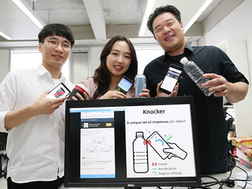 Object Identification and Interaction with a Smartphone Knock
(Professor Lee (far right) demonstrate 'Knocker' with his students.)
A KAIST team has featured a new technology, “Knocker”, which identifies objects and executes actions just by knocking on it with the smartphone. Software powered by machine learning of sounds, vibrations, and other reactions will perform the users’ directions.
What separates Knocker from existing technology is the sensor fusion of sound and motion. Previously, object identification used either computer vision technology with cameras or hardware such as RFID (Radio Frequency Identification) tags. These solutions all have their limitations. For computer vision technology, users need to take pictures of every item. Even worse, the technology will not work well in poor lighting situations. Using hardware leads to additional costs and labor burdens.
Knocker, on the other hand, can identify objects even in dark environments only with a smartphone, without requiring any specialized hardware or using a camera. Knocker utilizes the smartphone’s built-in sensors such as a microphone, an accelerometer, and a gyroscope to capture a unique set of responses generated when a smartphone is knocked against an object. Machine learning is used to analyze these responses and classify and identify objects.
The research team under Professor Sung-Ju Lee from the School of Computing confirmed the applicability of Knocker technology using 23 everyday objects such as books, laptop computers, water bottles, and bicycles. In noisy environments such as a busy café or on the side of a road, it achieved 83% identification accuracy. In a quiet indoor environment, the accuracy rose to 98%.
The team believes Knocker will open a new paradigm of object interaction. For instance, by knocking on an empty water bottle, a smartphone can automatically order new water bottles from a merchant app. When integrated with IoT devices, knocking on a bed’s headboard before going to sleep could turn off the lights and set an alarm. The team suggested and implemented 15 application cases in the paper, presented during the 2019 ACM International Joint Conference on Pervasive and Ubiquitous Computing (UbiComp 2019) held in London last month.
Professor Sung-Ju Lee said, “This new technology does not require any specialized sensor or hardware. It simply uses the built-in sensors on smartphones and takes advantage of the power of machine learning. It’s a software solution that everyday smartphone users could immediately benefit from.” He continued, “This technology enables users to conveniently interact with their favorite objects.”
The research was supported in part by the Next-Generation Information Computing Development Program through the National Research Foundation of Korea funded by the Ministry of Science and ICT and an Institute for Information & Communications Technology Promotion (IITP) grant funded by the Ministry of Science and ICT.
Figure: An example knock on a bottle. Knocker identifies the object by analyzing a unique set of responses from the knock, and automatically launches a proper application or service.
2019.10.02 View 29848
Object Identification and Interaction with a Smartphone Knock
(Professor Lee (far right) demonstrate 'Knocker' with his students.)
A KAIST team has featured a new technology, “Knocker”, which identifies objects and executes actions just by knocking on it with the smartphone. Software powered by machine learning of sounds, vibrations, and other reactions will perform the users’ directions.
What separates Knocker from existing technology is the sensor fusion of sound and motion. Previously, object identification used either computer vision technology with cameras or hardware such as RFID (Radio Frequency Identification) tags. These solutions all have their limitations. For computer vision technology, users need to take pictures of every item. Even worse, the technology will not work well in poor lighting situations. Using hardware leads to additional costs and labor burdens.
Knocker, on the other hand, can identify objects even in dark environments only with a smartphone, without requiring any specialized hardware or using a camera. Knocker utilizes the smartphone’s built-in sensors such as a microphone, an accelerometer, and a gyroscope to capture a unique set of responses generated when a smartphone is knocked against an object. Machine learning is used to analyze these responses and classify and identify objects.
The research team under Professor Sung-Ju Lee from the School of Computing confirmed the applicability of Knocker technology using 23 everyday objects such as books, laptop computers, water bottles, and bicycles. In noisy environments such as a busy café or on the side of a road, it achieved 83% identification accuracy. In a quiet indoor environment, the accuracy rose to 98%.
The team believes Knocker will open a new paradigm of object interaction. For instance, by knocking on an empty water bottle, a smartphone can automatically order new water bottles from a merchant app. When integrated with IoT devices, knocking on a bed’s headboard before going to sleep could turn off the lights and set an alarm. The team suggested and implemented 15 application cases in the paper, presented during the 2019 ACM International Joint Conference on Pervasive and Ubiquitous Computing (UbiComp 2019) held in London last month.
Professor Sung-Ju Lee said, “This new technology does not require any specialized sensor or hardware. It simply uses the built-in sensors on smartphones and takes advantage of the power of machine learning. It’s a software solution that everyday smartphone users could immediately benefit from.” He continued, “This technology enables users to conveniently interact with their favorite objects.”
The research was supported in part by the Next-Generation Information Computing Development Program through the National Research Foundation of Korea funded by the Ministry of Science and ICT and an Institute for Information & Communications Technology Promotion (IITP) grant funded by the Ministry of Science and ICT.
Figure: An example knock on a bottle. Knocker identifies the object by analyzing a unique set of responses from the knock, and automatically launches a proper application or service.
2019.10.02 View 29848 -
 Algorithm Identifies Optimal Pairs for Composing Metal-Organic Frameworks
The integration of metal-organic frameworks (MOFs) and other metal nanoparticles has increasingly led to the creation of new multifunctional materials. Many researchers have integrated MOFs with other classes of materials to produce new structures with synergetic properties.
Despite there being over 70,000 collections of synthesized MOFs that can be used as building blocks, the precise nature of the interaction and the bonding at the interface between the two materials still remains unknown. The question is how to sort out the right matching pairs out of 70,000 MOFs.
An algorithmic study published in Nature Communications by a KAIST research team presents a clue for finding the perfect pairs. The team, led by Professor Ji-Han Kim from the Department of Chemical and Biomolecular Engineering, developed a joint computational and experimental approach to rationally design MOF@MOFs, a composite of MOFs where an MOF is grown on a different MOF.
Professor Kim’s team, in collaboration with UNIST, noted that the metal node of one MOF can coordinately bond with the linker of a different MOF and the precisely matched interface configurations at atomic and molecular levels can enhance the likelihood of synthesizing MOF@MOFs.
They screened thousands of MOFs and identified optimal MOF pairs that can seamlessly connect to one another by taking advantage of the fact that the metal node of one MOF can form coordination bonds with the linkers of the second MOF. Six pairs predicted from the computational algorithm successfully grew into single crystals.
This computational workflow can readily extend into other classes of materials and can lead to the rapid exploration of the composite MOFs arena for accelerated materials development. Even more, the workflow can enhance the likelihood of synthesizing MOF@MOFs in the form of large single crystals, and thereby demonstrated the utility of rationally designing the MOF@MOFs.
This study is the first algorithm for predicting the synthesis of composite MOFs, to the best of their knowledge. Professor Kim said, “The number of predicted pairs can increase even more with the more general 2D lattice matching, and it is worth investigating in the future.”
This study was supported by Samsung Research Funding & Incubation Center of Samsung Electronics.
(Figure: An example of a rationally synthesized MOF@MOFs (cubic HKUST-1@MOF-5 ))
2019.08.30 View 17902
Algorithm Identifies Optimal Pairs for Composing Metal-Organic Frameworks
The integration of metal-organic frameworks (MOFs) and other metal nanoparticles has increasingly led to the creation of new multifunctional materials. Many researchers have integrated MOFs with other classes of materials to produce new structures with synergetic properties.
Despite there being over 70,000 collections of synthesized MOFs that can be used as building blocks, the precise nature of the interaction and the bonding at the interface between the two materials still remains unknown. The question is how to sort out the right matching pairs out of 70,000 MOFs.
An algorithmic study published in Nature Communications by a KAIST research team presents a clue for finding the perfect pairs. The team, led by Professor Ji-Han Kim from the Department of Chemical and Biomolecular Engineering, developed a joint computational and experimental approach to rationally design MOF@MOFs, a composite of MOFs where an MOF is grown on a different MOF.
Professor Kim’s team, in collaboration with UNIST, noted that the metal node of one MOF can coordinately bond with the linker of a different MOF and the precisely matched interface configurations at atomic and molecular levels can enhance the likelihood of synthesizing MOF@MOFs.
They screened thousands of MOFs and identified optimal MOF pairs that can seamlessly connect to one another by taking advantage of the fact that the metal node of one MOF can form coordination bonds with the linkers of the second MOF. Six pairs predicted from the computational algorithm successfully grew into single crystals.
This computational workflow can readily extend into other classes of materials and can lead to the rapid exploration of the composite MOFs arena for accelerated materials development. Even more, the workflow can enhance the likelihood of synthesizing MOF@MOFs in the form of large single crystals, and thereby demonstrated the utility of rationally designing the MOF@MOFs.
This study is the first algorithm for predicting the synthesis of composite MOFs, to the best of their knowledge. Professor Kim said, “The number of predicted pairs can increase even more with the more general 2D lattice matching, and it is worth investigating in the future.”
This study was supported by Samsung Research Funding & Incubation Center of Samsung Electronics.
(Figure: An example of a rationally synthesized MOF@MOFs (cubic HKUST-1@MOF-5 ))
2019.08.30 View 17902 -
 Researchers Describe a Mechanism Inducing Self-Killing of Cancer Cells
(Professor Kim (left) and lead author Lee)
Researchers have described a new mechanism which induces the self-killing of cancer cells by perturbing ion homeostasis. A research team from the Department of Biochemical Engineering has developed helical polypeptide potassium ionophores that lead to the onset of programmed cell death. The ionophores increase the active oxygen concentration to stress endoplasmic reticulum to the point of cellular death.
The electrochemical gradient between extracellular and intracellular conditions plays an important role in cell growth and metabolism. When a cell’s ion homeostasis is disturbed, critical functions accelerating the activation of apoptosis are inhibited in the cell.
Although ionophores have been intensively used as an ion homeostasis disturber, the mechanisms of cell death have been unclear and the bio-applicability has been limited. In the study featured at Advanced Science, the team presented an alpha helical peptide-based anticancer agent that is capable of transporting potassium ions with water solubility. The cationic, hydrophilic, and potassium ionic groups were combined at the end of the peptide side chain to provide both ion transport and hydrophilic properties.
These peptide-based ionophores reduce the intracellular potassium concentration and at the same time increase the intracellular calcium concentration. Increased intracellular calcium concentrations produce intracellular reactive oxygen species, causing endoplasmic reticulum stress, and ultimately leading to apoptosis.
Anticancer effects were evaluated using tumor-bearing mice to confirm the therapeutic effect, even in animal models. It was found that tumor growth was strongly inhibited by endoplasmic stress-mediated apoptosis.
Lead author Dr. Dae-Yong Lee said, “A peptide-based ionophore is more effective than conventional chemotherapeutic agents because it induces apoptosis via elevated reactive oxygen species levels. Professor Yeu-Chun Kim said he expects this new mechanism to be widely used as a new chemotherapeutic strategy. This research was funded by the National Research Foundation.
2019.08.28 View 21802
Researchers Describe a Mechanism Inducing Self-Killing of Cancer Cells
(Professor Kim (left) and lead author Lee)
Researchers have described a new mechanism which induces the self-killing of cancer cells by perturbing ion homeostasis. A research team from the Department of Biochemical Engineering has developed helical polypeptide potassium ionophores that lead to the onset of programmed cell death. The ionophores increase the active oxygen concentration to stress endoplasmic reticulum to the point of cellular death.
The electrochemical gradient between extracellular and intracellular conditions plays an important role in cell growth and metabolism. When a cell’s ion homeostasis is disturbed, critical functions accelerating the activation of apoptosis are inhibited in the cell.
Although ionophores have been intensively used as an ion homeostasis disturber, the mechanisms of cell death have been unclear and the bio-applicability has been limited. In the study featured at Advanced Science, the team presented an alpha helical peptide-based anticancer agent that is capable of transporting potassium ions with water solubility. The cationic, hydrophilic, and potassium ionic groups were combined at the end of the peptide side chain to provide both ion transport and hydrophilic properties.
These peptide-based ionophores reduce the intracellular potassium concentration and at the same time increase the intracellular calcium concentration. Increased intracellular calcium concentrations produce intracellular reactive oxygen species, causing endoplasmic reticulum stress, and ultimately leading to apoptosis.
Anticancer effects were evaluated using tumor-bearing mice to confirm the therapeutic effect, even in animal models. It was found that tumor growth was strongly inhibited by endoplasmic stress-mediated apoptosis.
Lead author Dr. Dae-Yong Lee said, “A peptide-based ionophore is more effective than conventional chemotherapeutic agents because it induces apoptosis via elevated reactive oxygen species levels. Professor Yeu-Chun Kim said he expects this new mechanism to be widely used as a new chemotherapeutic strategy. This research was funded by the National Research Foundation.
2019.08.28 View 21802 -
 Artificial Muscles Bloom, Dance, and Wave
Wearing a flower brooch that blooms before your eyes sounds like magic. KAIST researchers have made it real with robotic muscles.
Researchers have developed an ultrathin, artificial muscle for soft robotics. The advancement, recently reported in the journal Science Robotics, was demonstrated with a robotic blooming flower brooch, dancing robotic butterflies and fluttering tree leaves on a kinetic art piece.
The robotic equivalent of a muscle that can move is called an actuator. The actuator expands, contracts or rotates like muscle fibers using a stimulus such as electricity. Engineers around the world are striving to develop more dynamic actuators that respond quickly, can bend without breaking, and are very durable. Soft, robotic muscles could have a wide variety of applications, from wearable electronics to advanced prosthetics.
The team from KAIST’s Creative Research Initiative Center for Functionally Antagonistic Nano-Engineering developed a very thin, responsive, flexible and durable artificial muscle. The actuator looks like a skinny strip of paper about an inch long. They used a particular type of material called MXene, which is class of compounds that have layers only a few atoms thick.
Their chosen MXene material (T3C2Tx) is made of thin layers of titanium and carbon compounds. It was not flexible by itself; sheets of material would flake off the actuator when bent in a loop. That changed when the MXene was “ionically cross-linked” — connected through an ionic bond — to a synthetic polymer. The combination of materials made the actuator flexible, while still maintaining strength and conductivity, which is critical for movements driven by electricity.
Their particular combination performed better than others reported. Their actuator responded very quickly to low voltage, and lasted for more than five hours moving continuously.
To prove the tiny robotic muscle works, the team incorporated the actuator into wearable art: an origami-inspired brooch mimics how a narcissus flower unfolds its petals when a small amount of electricity is applied. They also designed robotic butterflies that move their wings up and down, and made the leaves of a tree sculpture flutter.
“Wearable robotics and kinetic art demonstrate how robotic muscles can have fun and beautiful applications,” said Il-Kwon Oh, lead paper author and professor of mechanical engineering. “It also shows the enormous potential for small, artificial muscles for a variety of uses, such as haptic feedback systems and active biomedical devices.”
The team next plans to investigate more practical applications of MXene-based soft actuators and other engineering applications of MXene 2D nanomaterials.
2019.08.22 View 26229
Artificial Muscles Bloom, Dance, and Wave
Wearing a flower brooch that blooms before your eyes sounds like magic. KAIST researchers have made it real with robotic muscles.
Researchers have developed an ultrathin, artificial muscle for soft robotics. The advancement, recently reported in the journal Science Robotics, was demonstrated with a robotic blooming flower brooch, dancing robotic butterflies and fluttering tree leaves on a kinetic art piece.
The robotic equivalent of a muscle that can move is called an actuator. The actuator expands, contracts or rotates like muscle fibers using a stimulus such as electricity. Engineers around the world are striving to develop more dynamic actuators that respond quickly, can bend without breaking, and are very durable. Soft, robotic muscles could have a wide variety of applications, from wearable electronics to advanced prosthetics.
The team from KAIST’s Creative Research Initiative Center for Functionally Antagonistic Nano-Engineering developed a very thin, responsive, flexible and durable artificial muscle. The actuator looks like a skinny strip of paper about an inch long. They used a particular type of material called MXene, which is class of compounds that have layers only a few atoms thick.
Their chosen MXene material (T3C2Tx) is made of thin layers of titanium and carbon compounds. It was not flexible by itself; sheets of material would flake off the actuator when bent in a loop. That changed when the MXene was “ionically cross-linked” — connected through an ionic bond — to a synthetic polymer. The combination of materials made the actuator flexible, while still maintaining strength and conductivity, which is critical for movements driven by electricity.
Their particular combination performed better than others reported. Their actuator responded very quickly to low voltage, and lasted for more than five hours moving continuously.
To prove the tiny robotic muscle works, the team incorporated the actuator into wearable art: an origami-inspired brooch mimics how a narcissus flower unfolds its petals when a small amount of electricity is applied. They also designed robotic butterflies that move their wings up and down, and made the leaves of a tree sculpture flutter.
“Wearable robotics and kinetic art demonstrate how robotic muscles can have fun and beautiful applications,” said Il-Kwon Oh, lead paper author and professor of mechanical engineering. “It also shows the enormous potential for small, artificial muscles for a variety of uses, such as haptic feedback systems and active biomedical devices.”
The team next plans to investigate more practical applications of MXene-based soft actuators and other engineering applications of MXene 2D nanomaterials.
2019.08.22 View 26229 -
 Highly Uniform and Low Hysteresis Pressure Sensor to Increase Practical Applicability
< Professor Steve Park (left) and the First Author Mr. Jinwon Oh (right) >
Researchers have designed a flexible pressure sensor that is expected to have a much wider applicability. A KAIST research team fabricated a piezoresistive pressure sensor of high uniformity with low hysteresis by chemically grafting a conductive polymer onto a porous elastomer template.
The team discovered that the uniformity of pore size and shape is directly related to the uniformity of the sensor. The team noted that by increasing pore size and shape variability, the variability of the sensor characteristics also increases.
Researchers led by Professor Steve Park from the Department of Materials Science and Engineering confirmed that compared to other sensors composed of randomly sized and shaped pores, which had a coefficient of variation in relative resistance change of 69.65%, their newly developed sensor exhibited much higher uniformity with a coefficient of variation of 2.43%. This study was reported in Small as the cover article on August 16.
Flexible pressure sensors have been actively researched and widely applied in electronic equipment such as touch screens, robots, wearable healthcare devices, electronic skin, and human-machine interfaces. In particular, piezoresistive pressure sensors based on elastomer‐conductive material composites hold significant potential due to their many advantages including a simple and low-cost fabrication process.
Various research results have been reported for ways to improve the performance of piezoresistive pressure sensors, most of which have been focused on increasing the sensitivity. Despite its significance, maximizing the sensitivity of composite-based piezoresistive pressure sensors is not necessary for many applications. On the other hand, sensor-to-sensor uniformity and hysteresis are two properties that are of critical importance to realize any application.
The importance of sensor-to-sensor uniformity is obvious. If the sensors manufactured under the same conditions have different properties, measurement reliability is compromised, and therefore the sensor cannot be used in a practical setting.
In addition, low hysteresis is also essential for improved measurement reliability. Hysteresis is a phenomenon in which the electrical readings differ depending on how fast or slow the sensor is being pressed, whether pressure is being released or applied, and how long and to what degree the sensor has been pressed. When a sensor has high hysteresis, the electrical readings will differ even under the same pressure, making the measurements unreliable.
Researchers said they observed a negligible hysteresis degree which was only 2%. This was attributed to the strong chemical bonding between the conductive polymer and the elastomer template, which prevents their relative sliding and displacement, and the porosity of the elastomer that enhances elastic behavior.
“This technology brings forth insight into how to address the two critical issues in pressure sensors: uniformity and hysteresis. We expect our technology to play an important role in increasing practical applications and the commercialization of pressure sensors in the near future,” said Professor Park.
This work was conducted as part of the KAIST‐funded Global Singularity Research Program for 2019, and also supported by the KUSTAR‐KAIST Institute.
Figure 1. Image of a porous elastomer template with uniform pore size and shape (left), Graph showing high uniformity in the sensors’ performance (right).
Figure 2. Hysteresis loops of the sensor at different pressure levels (left), and after a different number of cycles (right).
Figure 3. The cover page of Small Journal, Volume 15, Issue 33.
Publication:
Jinwon Oh, Jin‐Oh Kim, Yunjoo Kim, Han Byul Choi, Jun Chang Yang, Serin Lee, Mikhail Pyatykh, Jung Kim, Joo Yong Sim, and Steve Park. 2019. Highly Uniform and Low Hysteresis Piezoresistive Pressure Sensors Based on Chemical Grafting of Polypyrrole on Elastomer Template with Uniform Pore Size. Small. Wiley-VCH Verlag GmbH & Co. KgaA, Weinheim, Germany, Volume No. 15, Issue No. 33, Full Paper No. 201901744, 8 pages. https://doi.org/10.1002/smll.201901744
Profile: Prof. Steve Park, MS, PhD
stevepark@kaist.ac.kr
http://steveparklab.kaist.ac.kr/
Assistant Professor
Organic and Nano Electronics Laboratory
Department of Materials Science and Engineering
Korea Advanced Institute of Science and Technology (KAIST)
http://kaist.ac.kr
Daejeon 34141, Korea
Profile: Mr. Jinwon Oh, MS
jwoh1701@gmail.com
http://steveparklab.kaist.ac.kr/
Researcher
Organic and Nano Electronics Laboratory
Department of Materials Science and Engineering
Korea Advanced Institute of Science and Technology (KAIST)
http://kaist.ac.kr Daejeon 34141, Korea
Profile: Prof. Jung Kim, MS, PhD
jungkim@kaist.ac.kr
http://medev.kaist.ac.kr/
Professor
Biorobotics Laboratory
Department of Mechanical Engineering
Korea Advanced Institute of Science and Technology (KAIST)
http://kaist.ac.kr Daejeon 34141, Korea
Profile: Joo Yong Sim, PhD
jsim@etri.re.kr
Researcher
Bio-Medical IT Convergence Research Department
Electronics and Telecommunications Research Institute (ETRI)
https://www.etri.re.krDaejeon 34129, Korea
(END)
2019.08.19 View 29392
Highly Uniform and Low Hysteresis Pressure Sensor to Increase Practical Applicability
< Professor Steve Park (left) and the First Author Mr. Jinwon Oh (right) >
Researchers have designed a flexible pressure sensor that is expected to have a much wider applicability. A KAIST research team fabricated a piezoresistive pressure sensor of high uniformity with low hysteresis by chemically grafting a conductive polymer onto a porous elastomer template.
The team discovered that the uniformity of pore size and shape is directly related to the uniformity of the sensor. The team noted that by increasing pore size and shape variability, the variability of the sensor characteristics also increases.
Researchers led by Professor Steve Park from the Department of Materials Science and Engineering confirmed that compared to other sensors composed of randomly sized and shaped pores, which had a coefficient of variation in relative resistance change of 69.65%, their newly developed sensor exhibited much higher uniformity with a coefficient of variation of 2.43%. This study was reported in Small as the cover article on August 16.
Flexible pressure sensors have been actively researched and widely applied in electronic equipment such as touch screens, robots, wearable healthcare devices, electronic skin, and human-machine interfaces. In particular, piezoresistive pressure sensors based on elastomer‐conductive material composites hold significant potential due to their many advantages including a simple and low-cost fabrication process.
Various research results have been reported for ways to improve the performance of piezoresistive pressure sensors, most of which have been focused on increasing the sensitivity. Despite its significance, maximizing the sensitivity of composite-based piezoresistive pressure sensors is not necessary for many applications. On the other hand, sensor-to-sensor uniformity and hysteresis are two properties that are of critical importance to realize any application.
The importance of sensor-to-sensor uniformity is obvious. If the sensors manufactured under the same conditions have different properties, measurement reliability is compromised, and therefore the sensor cannot be used in a practical setting.
In addition, low hysteresis is also essential for improved measurement reliability. Hysteresis is a phenomenon in which the electrical readings differ depending on how fast or slow the sensor is being pressed, whether pressure is being released or applied, and how long and to what degree the sensor has been pressed. When a sensor has high hysteresis, the electrical readings will differ even under the same pressure, making the measurements unreliable.
Researchers said they observed a negligible hysteresis degree which was only 2%. This was attributed to the strong chemical bonding between the conductive polymer and the elastomer template, which prevents their relative sliding and displacement, and the porosity of the elastomer that enhances elastic behavior.
“This technology brings forth insight into how to address the two critical issues in pressure sensors: uniformity and hysteresis. We expect our technology to play an important role in increasing practical applications and the commercialization of pressure sensors in the near future,” said Professor Park.
This work was conducted as part of the KAIST‐funded Global Singularity Research Program for 2019, and also supported by the KUSTAR‐KAIST Institute.
Figure 1. Image of a porous elastomer template with uniform pore size and shape (left), Graph showing high uniformity in the sensors’ performance (right).
Figure 2. Hysteresis loops of the sensor at different pressure levels (left), and after a different number of cycles (right).
Figure 3. The cover page of Small Journal, Volume 15, Issue 33.
Publication:
Jinwon Oh, Jin‐Oh Kim, Yunjoo Kim, Han Byul Choi, Jun Chang Yang, Serin Lee, Mikhail Pyatykh, Jung Kim, Joo Yong Sim, and Steve Park. 2019. Highly Uniform and Low Hysteresis Piezoresistive Pressure Sensors Based on Chemical Grafting of Polypyrrole on Elastomer Template with Uniform Pore Size. Small. Wiley-VCH Verlag GmbH & Co. KgaA, Weinheim, Germany, Volume No. 15, Issue No. 33, Full Paper No. 201901744, 8 pages. https://doi.org/10.1002/smll.201901744
Profile: Prof. Steve Park, MS, PhD
stevepark@kaist.ac.kr
http://steveparklab.kaist.ac.kr/
Assistant Professor
Organic and Nano Electronics Laboratory
Department of Materials Science and Engineering
Korea Advanced Institute of Science and Technology (KAIST)
http://kaist.ac.kr
Daejeon 34141, Korea
Profile: Mr. Jinwon Oh, MS
jwoh1701@gmail.com
http://steveparklab.kaist.ac.kr/
Researcher
Organic and Nano Electronics Laboratory
Department of Materials Science and Engineering
Korea Advanced Institute of Science and Technology (KAIST)
http://kaist.ac.kr Daejeon 34141, Korea
Profile: Prof. Jung Kim, MS, PhD
jungkim@kaist.ac.kr
http://medev.kaist.ac.kr/
Professor
Biorobotics Laboratory
Department of Mechanical Engineering
Korea Advanced Institute of Science and Technology (KAIST)
http://kaist.ac.kr Daejeon 34141, Korea
Profile: Joo Yong Sim, PhD
jsim@etri.re.kr
Researcher
Bio-Medical IT Convergence Research Department
Electronics and Telecommunications Research Institute (ETRI)
https://www.etri.re.krDaejeon 34129, Korea
(END)
2019.08.19 View 29392 -
 Accurate Detection of Low-Level Somatic Mutation in Intractable Epilepsy
KAIST medical scientists have developed an advanced method for perfectly detecting low-level somatic mutation in patients with intractable epilepsy. Their study showed that deep sequencing replicates of major focal epilepsy genes accurately and efficiently identified low-level somatic mutations in intractable epilepsy.
According to the study, their diagnostic method could increase the accuracy up to 100%, unlike the conventional sequencing analysis, which stands at about 30% accuracy. This work was published in Acta Neuropathologica.
Epilepsy is a neurological disorder common in children. Approximately one third of child patients are diagnosed with intractable epilepsy despite adequate anti-epileptic medication treatment.
Somatic mutations in mTOR pathway genes, SLC35A2, and BRAF are the major genetic causes of intractable epilepsies. A clinical trial to target Focal Cortical Dysplasia type II (FCDII), the mTOR inhibitor is underway at Severance Hospital, their collaborator in Seoul, Korea. However, it is difficult to detect such somatic mutations causing intractable epilepsy because their mutational burden is less than 5%, which is similar to the level of sequencing artifacts. In the clinical field, this has remained a standing challenge for the genetic diagnosis of somatic mutations in intractable epilepsy.
Professor Jeong Ho Lee’s team at the Graduate School of Medical Science and Engineering analyzed paired brain and peripheral tissues from 232 intractable epilepsy patients with various brain pathologies at Severance Hospital using deep sequencing and extracted the major focal epilepsy genes.
They narrowed down target genes to eight major focal epilepsy genes, eliminating almost all of the false positive calls using deep targeted sequencing. As a result, the advanced method robustly increased the accuracy and enabled them to detect low-level somatic mutations in unmatched Formalin Fixed Paraffin Embedded (FFPE) brain samples, the most clinically relevant samples.
Professor Lee conducted this study in collaboration with Professor Dong Suk Kim and Hoon-Chul Kang at Severance Hospital of Yonsei University. He said, “This advanced method of genetic analysis will improve overall patient care by providing more comprehensive genetic counseling and informing decisions on alternative treatments.”
Professor Lee has investigated low-level somatic mutations arising in the brain for a decade. He is developing innovative diagnostics and therapeutics for untreatable brain disorders including intractable epilepsy and glioblastoma at a tech-startup called SoVarGen. “All of the technologies we used during the research were transferred to the company. This research gave us very good momentum to reach the next phase of our startup,” he remarked.
The work was supported by grants from the Suh Kyungbae Foundation, a National Research Foundation of Korea grant funded by the Ministry of Science and ICT, the Korean Health Technology R&D Project from the Ministry of Health & Welfare, and the Netherlands Organization for Health Research and Development.
(Figure: Landscape of somatic and germline mutations identified in intractable epilepsy patients. a Signaling pathways for all of the mutated genes identified in this study. Bold: somatic mutation, Regular: germline mutation. b The distribution of variant allelic frequencies (VAFs) of identified somatic mutations. c The detecting rate and types of identified mutations according to histopathology. Yellow: somatic mutations, green: two-hit mutations, grey: germline mutations.)
2019.08.14 View 30197
Accurate Detection of Low-Level Somatic Mutation in Intractable Epilepsy
KAIST medical scientists have developed an advanced method for perfectly detecting low-level somatic mutation in patients with intractable epilepsy. Their study showed that deep sequencing replicates of major focal epilepsy genes accurately and efficiently identified low-level somatic mutations in intractable epilepsy.
According to the study, their diagnostic method could increase the accuracy up to 100%, unlike the conventional sequencing analysis, which stands at about 30% accuracy. This work was published in Acta Neuropathologica.
Epilepsy is a neurological disorder common in children. Approximately one third of child patients are diagnosed with intractable epilepsy despite adequate anti-epileptic medication treatment.
Somatic mutations in mTOR pathway genes, SLC35A2, and BRAF are the major genetic causes of intractable epilepsies. A clinical trial to target Focal Cortical Dysplasia type II (FCDII), the mTOR inhibitor is underway at Severance Hospital, their collaborator in Seoul, Korea. However, it is difficult to detect such somatic mutations causing intractable epilepsy because their mutational burden is less than 5%, which is similar to the level of sequencing artifacts. In the clinical field, this has remained a standing challenge for the genetic diagnosis of somatic mutations in intractable epilepsy.
Professor Jeong Ho Lee’s team at the Graduate School of Medical Science and Engineering analyzed paired brain and peripheral tissues from 232 intractable epilepsy patients with various brain pathologies at Severance Hospital using deep sequencing and extracted the major focal epilepsy genes.
They narrowed down target genes to eight major focal epilepsy genes, eliminating almost all of the false positive calls using deep targeted sequencing. As a result, the advanced method robustly increased the accuracy and enabled them to detect low-level somatic mutations in unmatched Formalin Fixed Paraffin Embedded (FFPE) brain samples, the most clinically relevant samples.
Professor Lee conducted this study in collaboration with Professor Dong Suk Kim and Hoon-Chul Kang at Severance Hospital of Yonsei University. He said, “This advanced method of genetic analysis will improve overall patient care by providing more comprehensive genetic counseling and informing decisions on alternative treatments.”
Professor Lee has investigated low-level somatic mutations arising in the brain for a decade. He is developing innovative diagnostics and therapeutics for untreatable brain disorders including intractable epilepsy and glioblastoma at a tech-startup called SoVarGen. “All of the technologies we used during the research were transferred to the company. This research gave us very good momentum to reach the next phase of our startup,” he remarked.
The work was supported by grants from the Suh Kyungbae Foundation, a National Research Foundation of Korea grant funded by the Ministry of Science and ICT, the Korean Health Technology R&D Project from the Ministry of Health & Welfare, and the Netherlands Organization for Health Research and Development.
(Figure: Landscape of somatic and germline mutations identified in intractable epilepsy patients. a Signaling pathways for all of the mutated genes identified in this study. Bold: somatic mutation, Regular: germline mutation. b The distribution of variant allelic frequencies (VAFs) of identified somatic mutations. c The detecting rate and types of identified mutations according to histopathology. Yellow: somatic mutations, green: two-hit mutations, grey: germline mutations.)
2019.08.14 View 30197 -
 Enhanced Natural Gas Storage to Help Reduce Global Warming
< Professor Atilhan (left) and Professor Yavuz (right) >
Researchers have designed plastic-based materials that can store natural gas more effectively. These new materials can not only make large-scale, cost-effective, and safe natural gas storage possible, but further hold a strong promise for combating global warming.
Natural gas (predominantly methane) is a clean energy alternative. It is stored by compression, liquefaction, or adsorption. Among these, adsorbed natural gas (ANG) storage is a more efficient, cheaper, and safer alternative to conventional compressed natural gas (CNG) and liquefied natural gas (LNG) storage approaches that have drawbacks such as low storage efficiency, high costs, and safety concerns. However, developing adsorptive materials that can more fully exploit the advantages of ANG storage has remained a challenging task.
A KAIST research team led by Professor Cafer T. Yavuz from the Graduate School of Energy, Environment, Water, and Sustainability (EEWS), in collaboration with Professor Mert Atilhan’s group from Texas A&M University, synthesized 29 unique porous polymeric structures with inherent flexibility, and tested their methane gas uptake capacity at high pressures. These porous polymers had varying synthetic complexities, porosities, and morphologies, and the researchers subjected each porous polymer to pure methane gas under various conditions to study the ANG performances.
Of these 29 distinct chemical structures, COP-150 was particularly noteworthy as it achieved a high deliverable gravimetric methane working capacity when cycled between 5 and 100 bar at 273 K, which is 98% of the total uptake capacity. This result surpassed the target set by the United States Department of Energy (US DOE).
COP-150 is the first ever structure to fulfil both the gravimetric and volumetric requirements of the US DOE for successful vehicular use, and the total cost to produce the COP-150 adsorbent was only 1 USD per kilogram.
COP-150 can be produced using freely available and easily accessible plastic materials, and moreover, its synthesis takes place at room temperature, open to the air, and no previous purification of the chemicals is required. The pressure-triggered flexible structure of COP-150 is also advantageous in terms of the total working capacity of deliverable methane for real applications.
The research team believed that the increased pressure flexes the network structure of COP-150 showing “swelling” behavior, and suggested that the flexibility provides rapid desorption and thermal management, while the hydrophobicity and the nature of the covalently bonded framework allow these promising materials to tolerate harsh conditions.
This swelling mechanism of expansion-contraction solves two other major issues, the team noted. Firstly, when using adsorbents based on such a mechanism, unsafe pressure spikes that may occur due to temperature swings can be eliminated. In addition, contamination can also be minimized, since the adsorbent remains contracted when no gas is stored.
Professor Yavuz said, “We envision a whole host of new designs and mechanisms to be developed based on our concept. Since natural gas is a much cleaner fuel than coal and petroleum, new developments in this realm will help switching to the use of less polluting fuels.”
Professor Atilhan agreed the most important impact of their research is on the environment. “Using natural gas more than coal and petroleum will significantly reduce greenhouse gas emissions. We believe, one day, we might see vehicles equipped with our materials that are run by a cleaner natural gas fuel,” he added.
This study, reported in Nature Energy on July 8, was supported by National Research Foundation of Korea (NRF) grants ( NRF-2016R1A2B4011027, NRF-2017M3A7B4042140, and NRF-2017M3A7B4042235).
< Suggested chemical structure of COP-150 >
< Initial ingredients (left) and final product (right) of COP-150 synthesis >
< Comparison of highest reported volumetric working capacities >
(END)
2019.08.09 View 28125
Enhanced Natural Gas Storage to Help Reduce Global Warming
< Professor Atilhan (left) and Professor Yavuz (right) >
Researchers have designed plastic-based materials that can store natural gas more effectively. These new materials can not only make large-scale, cost-effective, and safe natural gas storage possible, but further hold a strong promise for combating global warming.
Natural gas (predominantly methane) is a clean energy alternative. It is stored by compression, liquefaction, or adsorption. Among these, adsorbed natural gas (ANG) storage is a more efficient, cheaper, and safer alternative to conventional compressed natural gas (CNG) and liquefied natural gas (LNG) storage approaches that have drawbacks such as low storage efficiency, high costs, and safety concerns. However, developing adsorptive materials that can more fully exploit the advantages of ANG storage has remained a challenging task.
A KAIST research team led by Professor Cafer T. Yavuz from the Graduate School of Energy, Environment, Water, and Sustainability (EEWS), in collaboration with Professor Mert Atilhan’s group from Texas A&M University, synthesized 29 unique porous polymeric structures with inherent flexibility, and tested their methane gas uptake capacity at high pressures. These porous polymers had varying synthetic complexities, porosities, and morphologies, and the researchers subjected each porous polymer to pure methane gas under various conditions to study the ANG performances.
Of these 29 distinct chemical structures, COP-150 was particularly noteworthy as it achieved a high deliverable gravimetric methane working capacity when cycled between 5 and 100 bar at 273 K, which is 98% of the total uptake capacity. This result surpassed the target set by the United States Department of Energy (US DOE).
COP-150 is the first ever structure to fulfil both the gravimetric and volumetric requirements of the US DOE for successful vehicular use, and the total cost to produce the COP-150 adsorbent was only 1 USD per kilogram.
COP-150 can be produced using freely available and easily accessible plastic materials, and moreover, its synthesis takes place at room temperature, open to the air, and no previous purification of the chemicals is required. The pressure-triggered flexible structure of COP-150 is also advantageous in terms of the total working capacity of deliverable methane for real applications.
The research team believed that the increased pressure flexes the network structure of COP-150 showing “swelling” behavior, and suggested that the flexibility provides rapid desorption and thermal management, while the hydrophobicity and the nature of the covalently bonded framework allow these promising materials to tolerate harsh conditions.
This swelling mechanism of expansion-contraction solves two other major issues, the team noted. Firstly, when using adsorbents based on such a mechanism, unsafe pressure spikes that may occur due to temperature swings can be eliminated. In addition, contamination can also be minimized, since the adsorbent remains contracted when no gas is stored.
Professor Yavuz said, “We envision a whole host of new designs and mechanisms to be developed based on our concept. Since natural gas is a much cleaner fuel than coal and petroleum, new developments in this realm will help switching to the use of less polluting fuels.”
Professor Atilhan agreed the most important impact of their research is on the environment. “Using natural gas more than coal and petroleum will significantly reduce greenhouse gas emissions. We believe, one day, we might see vehicles equipped with our materials that are run by a cleaner natural gas fuel,” he added.
This study, reported in Nature Energy on July 8, was supported by National Research Foundation of Korea (NRF) grants ( NRF-2016R1A2B4011027, NRF-2017M3A7B4042140, and NRF-2017M3A7B4042235).
< Suggested chemical structure of COP-150 >
< Initial ingredients (left) and final product (right) of COP-150 synthesis >
< Comparison of highest reported volumetric working capacities >
(END)
2019.08.09 View 28125 -
 Manipulating Brain Cells by Smartphone
Researchers have developed a soft neural implant that can be wirelessly controlled using a smartphone. It is the first wireless neural device capable of indefinitely delivering multiple drugs and multiple colour lights, which neuroscientists believe can speed up efforts to uncover brain diseases such as Parkinson’s, Alzheimer’s, addiction, depression, and pain.
A team under Professor Jae-Woong Jeong from the School of Electrical Engineering at KAIST and his collaborators have invented a device that can control neural circuits using a tiny brain implant controlled by a smartphone. The device, using Lego-like replaceable drug cartridges and powerful, low-energy Bluetooth, can target specific neurons of interest using drugs and light for prolonged periods. This study was published in Nature Biomedical Engineering.
“This novel device is the fruit of advanced electronics design and powerful micro and nanoscale engineering,” explained Professor Jeong. “We are interested in further developing this technology to make a brain implant for clinical applications.”
This technology significantly overshadows the conventional methods used by neuroscientists, which usually involve rigid metal tubes and optical fibers to deliver drugs and light. Apart from limiting the subject’s movement due to bulky equipment, their relatively rigid structure causes lesions in soft brain tissue over time, therefore making them not suitable for long-term implantation. Although some efforts have been made to partly mitigate adverse tissue response by incorporating soft probes and wireless platforms, the previous solutions were limited by their inability to deliver drugs for long periods of time as well as their bulky and complex control setups.
To achieve chronic wireless drug delivery, scientists had to solve the critical challenge of the exhaustion and evaporation of drugs. To combat this, the researchers invented a neural device with a replaceable drug cartridge, which could allow neuroscientists to study the same brain circuits for several months without worrying about running out of drugs.
These ‘plug-n-play’ drug cartridges were assembled into a brain implant for mice with a soft and ultrathin probe (with the thickness of a human hair), which consisted of microfluidic channels and tiny LEDs (smaller than a grain of salt), for unlimited drug doses and light delivery.
Controlled with an elegant and simple user interface on a smartphone, neuroscientists can easily trigger any specific combination or precise sequencing of light and drug delivery in any implanted target animal without the need to be physically inside the laboratory. Using these wireless neural devices, researchers can also easily setup fully automated animal studies where the behaviour of one animal could affect other animals by triggering light and/or drug delivery.
“The wireless neural device enables chronic chemical and optical neuromodulation that has never been achieved before,” said lead author Raza Qazi, a researcher with KAIST and the University of Colorado Boulder.
This work was supported by grants from the National Research Foundation of Korea, US National Institute of Health, National Institute on Drug Abuse, and Mallinckrodt Professorship.
(A neural implant with replaceable drug cartridges and Bluetooth low-energy can target specific neurons .)
(Micro LED controlling using smartphone application)
2019.08.07 View 33950
Manipulating Brain Cells by Smartphone
Researchers have developed a soft neural implant that can be wirelessly controlled using a smartphone. It is the first wireless neural device capable of indefinitely delivering multiple drugs and multiple colour lights, which neuroscientists believe can speed up efforts to uncover brain diseases such as Parkinson’s, Alzheimer’s, addiction, depression, and pain.
A team under Professor Jae-Woong Jeong from the School of Electrical Engineering at KAIST and his collaborators have invented a device that can control neural circuits using a tiny brain implant controlled by a smartphone. The device, using Lego-like replaceable drug cartridges and powerful, low-energy Bluetooth, can target specific neurons of interest using drugs and light for prolonged periods. This study was published in Nature Biomedical Engineering.
“This novel device is the fruit of advanced electronics design and powerful micro and nanoscale engineering,” explained Professor Jeong. “We are interested in further developing this technology to make a brain implant for clinical applications.”
This technology significantly overshadows the conventional methods used by neuroscientists, which usually involve rigid metal tubes and optical fibers to deliver drugs and light. Apart from limiting the subject’s movement due to bulky equipment, their relatively rigid structure causes lesions in soft brain tissue over time, therefore making them not suitable for long-term implantation. Although some efforts have been made to partly mitigate adverse tissue response by incorporating soft probes and wireless platforms, the previous solutions were limited by their inability to deliver drugs for long periods of time as well as their bulky and complex control setups.
To achieve chronic wireless drug delivery, scientists had to solve the critical challenge of the exhaustion and evaporation of drugs. To combat this, the researchers invented a neural device with a replaceable drug cartridge, which could allow neuroscientists to study the same brain circuits for several months without worrying about running out of drugs.
These ‘plug-n-play’ drug cartridges were assembled into a brain implant for mice with a soft and ultrathin probe (with the thickness of a human hair), which consisted of microfluidic channels and tiny LEDs (smaller than a grain of salt), for unlimited drug doses and light delivery.
Controlled with an elegant and simple user interface on a smartphone, neuroscientists can easily trigger any specific combination or precise sequencing of light and drug delivery in any implanted target animal without the need to be physically inside the laboratory. Using these wireless neural devices, researchers can also easily setup fully automated animal studies where the behaviour of one animal could affect other animals by triggering light and/or drug delivery.
“The wireless neural device enables chronic chemical and optical neuromodulation that has never been achieved before,” said lead author Raza Qazi, a researcher with KAIST and the University of Colorado Boulder.
This work was supported by grants from the National Research Foundation of Korea, US National Institute of Health, National Institute on Drug Abuse, and Mallinckrodt Professorship.
(A neural implant with replaceable drug cartridges and Bluetooth low-energy can target specific neurons .)
(Micro LED controlling using smartphone application)
2019.08.07 View 33950 -
 Synthesizing Single-Crystalline Hexagonal Graphene Quantum Dots
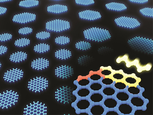
(Figure: Uniformly ordered single-crystalline graphene quantum dots of various sizes synthesized through solution chemistry.)
A KAIST team has designed a novel strategy for synthesizing single-crystalline graphene quantum dots, which emit stable blue light. The research team confirmed that a display made of their synthesized graphene quantum dots successfully emitted blue light with stable electric pressure, reportedly resolving the long-standing challenges of blue light emission in manufactured displays. The study, led by Professor O Ok Park in the Department of Chemical and Biological Engineering, was featured online in Nano Letters on July 5.
Graphene has gained increased attention as a next-generation material for its heat and electrical conductivity as well as its transparency. However, single and multi-layered graphene have characteristics of a conductor so that it is difficult to apply into semiconductor. Only when downsized to the nanoscale, semiconductor’s distinct feature of bandgap will be exhibited to emit the light in the graphene. This illuminating featuring of dot is referred to as a graphene quantum dot.
Conventionally, single-crystalline graphene has been fabricated by chemical vapor deposition (CVD) on copper or nickel thin films, or by peeling graphite physically and chemically. However, graphene made via chemical vapor deposition is mainly used for large-surface transparent electrodes. Meanwhile, graphene made by chemical and physical peeling carries uneven size defects.
The research team explained that their graphene quantum dots exhibited a very stable single-phase reaction when they mixed amine and acetic acid with an aqueous solution of glucose. Then, they synthesized single-crystalline graphene quantum dots from the self-assembly of the reaction intermediate. In the course of fabrication, the team developed a new separation method at a low-temperature precipitation, which led to successfully creating a homogeneous nucleation of graphene quantum dots via a single-phase reaction.
Professor Park and his colleagues have developed solution phase synthesis technology that allows for the creation of the desired crystal size for single nanocrystals down to 100 nano meters. It is reportedly the first synthesis of the homogeneous nucleation of graphene through a single-phase reaction.
Professor Park said, "This solution method will significantly contribute to the grafting of graphene in various fields. The application of this new graphene will expand the scope of its applications such as for flexible displays and varistors.”
This research was a joint project with a team from Korea University under Professor Sang Hyuk Im from the Department of Chemical and Biological Engineering, and was supported by the National Research Foundation of Korea, the Nano-Material Technology Development Program from the Electronics and Telecommunications Research Institute (ETRI), KAIST EEWS, and the BK21+ project from the Korean government.
2019.08.02 View 35279
Synthesizing Single-Crystalline Hexagonal Graphene Quantum Dots
(Figure: Uniformly ordered single-crystalline graphene quantum dots of various sizes synthesized through solution chemistry.)
A KAIST team has designed a novel strategy for synthesizing single-crystalline graphene quantum dots, which emit stable blue light. The research team confirmed that a display made of their synthesized graphene quantum dots successfully emitted blue light with stable electric pressure, reportedly resolving the long-standing challenges of blue light emission in manufactured displays. The study, led by Professor O Ok Park in the Department of Chemical and Biological Engineering, was featured online in Nano Letters on July 5.
Graphene has gained increased attention as a next-generation material for its heat and electrical conductivity as well as its transparency. However, single and multi-layered graphene have characteristics of a conductor so that it is difficult to apply into semiconductor. Only when downsized to the nanoscale, semiconductor’s distinct feature of bandgap will be exhibited to emit the light in the graphene. This illuminating featuring of dot is referred to as a graphene quantum dot.
Conventionally, single-crystalline graphene has been fabricated by chemical vapor deposition (CVD) on copper or nickel thin films, or by peeling graphite physically and chemically. However, graphene made via chemical vapor deposition is mainly used for large-surface transparent electrodes. Meanwhile, graphene made by chemical and physical peeling carries uneven size defects.
The research team explained that their graphene quantum dots exhibited a very stable single-phase reaction when they mixed amine and acetic acid with an aqueous solution of glucose. Then, they synthesized single-crystalline graphene quantum dots from the self-assembly of the reaction intermediate. In the course of fabrication, the team developed a new separation method at a low-temperature precipitation, which led to successfully creating a homogeneous nucleation of graphene quantum dots via a single-phase reaction.
Professor Park and his colleagues have developed solution phase synthesis technology that allows for the creation of the desired crystal size for single nanocrystals down to 100 nano meters. It is reportedly the first synthesis of the homogeneous nucleation of graphene through a single-phase reaction.
Professor Park said, "This solution method will significantly contribute to the grafting of graphene in various fields. The application of this new graphene will expand the scope of its applications such as for flexible displays and varistors.”
This research was a joint project with a team from Korea University under Professor Sang Hyuk Im from the Department of Chemical and Biological Engineering, and was supported by the National Research Foundation of Korea, the Nano-Material Technology Development Program from the Electronics and Telecommunications Research Institute (ETRI), KAIST EEWS, and the BK21+ project from the Korean government.
2019.08.02 View 35279 -
 Newly Identified Meningeal Lymphatic Vessels Answers the Key Questions on Brain Clearance
(Figure: Schematic images of location and features of meningeal lymphatic vessels and their changes associated with ageing.)
Just see what happens when your neighborhood’s waste disposal system is out of service. Not only do the piles of trash stink but they can indeed hinder the area’s normal functioning. That is also the case when the brain’s waste management is on the blink.
The buildup of toxic proteins in the brain causes a massive damage to the nerves, leading to cognitive dysfunction and increased probability of developing neurodegenerative disorders such as Alzheimer's disease. Though the brain drains its waste via the cerebrospinal fluid (CSF), little has been understood about an accurate route for the brain’s cleansing mechanism.
Medical scientists led by Professor Gou Young Koh at the Graduate School of Medical Science and Engineering have reported the basal side of the skull as the major route, so called “hotspot” for CSF drainage.
They found that basal meningeal lymphatic vessels (mLVs) function as the main plumbing pipes for CSF. They confirmed macromolecules in the CSF mainly runs through the basal mLVs. Notably, the team also revealed that the brain’s major drainage system, specifically basal mLVs are impaired with aging. Their findings have been reported in the journal Nature on July 24.
Throughout our body, excess fluids and waste products are removed from tissues via lymphatic vessels. It was only recently discovered that the brain also has a lymphatic drainage system. mLVs are supposed to carry waste from the brain tissue fluid and the CSF down the deep cervical lymph nodes for disposal. Still scientist are left with one perplexing question — where is the main exit for the CSF? Though mLVs in the upper part of the skull (dorsal meningeal lymphatic vessels) were reported as the brain’s clearance pathways in 2014, no substantial drainage mechanism was observed in that section.
“As a hidden exit for CSF, we looked into the mLVs trapped within complex structures at the base of the skull,” says Dr. Ji Hoon Ahn, the first author of this study. The researchers used several techniques to characterize the basal mLVs in detail. They used a genetically engineered lymphatic-reporter mouse model to visualize mLVs under a fluorescence microscope. By performing a careful examination of the mice skull, they found distinctive features of basal mLVs that make them suitable for CSF uptake and drainage. Just like typical functional lymphatic vessels, basal mLVs are found to have abundant lymphatic vessel branches with finger-like protrusions. Additionally, valves inside the basal mLVs allow the flow to go in one direction. In particular, they found that the basal mLVs are closely located to the CSF. Dr. Hyunsoo Cho, the first author of this study explains, “All up, it seemed a solid case that basal mLVs are the brain’s main clearance pathways.
The researchers verified such specialized morphologic characteristics of basal mLVs indeed facilitate the CSF uptake and drainage. Using CSF contrast-enhanced magnetic resonance imaging in a rat model, they found that CSF is drained preferentially through the basal mLVs. They also utilized a lymphatic-reporter mouse model and discovered that fluorescence-tagged tracer injected into the brain itself or the CSF is cleared mainly through the basal mLVs. Jun-Hee Kim, the first author of this study notes, “We literally saw that the brain clearance mechanism utilizing basal outflow route to exit the skull.
It has long been suggested that CSF turnover and drainage declines with ageing. However, alteration of mLVs associated with ageing is poorly understood. In this study, the researchers observed changes of mLVs in young (3-month-old) and aged (24~27-months-old) mice. They found that the structure of the basal mLVs and their lymphatic valves in aged mice become severely flawed, thus hampering CSF clearance. The corresponding author of this study, Dr. Koh says, “By characterizing the precise route for fluids leaving the brain, this study improves our understanding on how waste is cleared from the brain. Our findings also provide further insights into the role of impaired CSF clearance in the development of age-related neurodegenerative diseases.”
Many current therapies for Alzheimer’s disease target abnormally accumulated proteins, such as beta-amyloid. By mapping out a precise route for the brain’s waste clearance system, this study may be able to help find ways to improve the brain’s cleansing function. Such breakthrough might become quite a sensational strategy for eliminating the buildup of aging-related toxic proteins. “It definitely warrants more extensive investigation of mLVs in patients with age-related neurodegenerative disease such as Alzheimer’s disease prior to clinical investigation,” adds Professor Koh.
2019.07.25 View 33608
Newly Identified Meningeal Lymphatic Vessels Answers the Key Questions on Brain Clearance
(Figure: Schematic images of location and features of meningeal lymphatic vessels and their changes associated with ageing.)
Just see what happens when your neighborhood’s waste disposal system is out of service. Not only do the piles of trash stink but they can indeed hinder the area’s normal functioning. That is also the case when the brain’s waste management is on the blink.
The buildup of toxic proteins in the brain causes a massive damage to the nerves, leading to cognitive dysfunction and increased probability of developing neurodegenerative disorders such as Alzheimer's disease. Though the brain drains its waste via the cerebrospinal fluid (CSF), little has been understood about an accurate route for the brain’s cleansing mechanism.
Medical scientists led by Professor Gou Young Koh at the Graduate School of Medical Science and Engineering have reported the basal side of the skull as the major route, so called “hotspot” for CSF drainage.
They found that basal meningeal lymphatic vessels (mLVs) function as the main plumbing pipes for CSF. They confirmed macromolecules in the CSF mainly runs through the basal mLVs. Notably, the team also revealed that the brain’s major drainage system, specifically basal mLVs are impaired with aging. Their findings have been reported in the journal Nature on July 24.
Throughout our body, excess fluids and waste products are removed from tissues via lymphatic vessels. It was only recently discovered that the brain also has a lymphatic drainage system. mLVs are supposed to carry waste from the brain tissue fluid and the CSF down the deep cervical lymph nodes for disposal. Still scientist are left with one perplexing question — where is the main exit for the CSF? Though mLVs in the upper part of the skull (dorsal meningeal lymphatic vessels) were reported as the brain’s clearance pathways in 2014, no substantial drainage mechanism was observed in that section.
“As a hidden exit for CSF, we looked into the mLVs trapped within complex structures at the base of the skull,” says Dr. Ji Hoon Ahn, the first author of this study. The researchers used several techniques to characterize the basal mLVs in detail. They used a genetically engineered lymphatic-reporter mouse model to visualize mLVs under a fluorescence microscope. By performing a careful examination of the mice skull, they found distinctive features of basal mLVs that make them suitable for CSF uptake and drainage. Just like typical functional lymphatic vessels, basal mLVs are found to have abundant lymphatic vessel branches with finger-like protrusions. Additionally, valves inside the basal mLVs allow the flow to go in one direction. In particular, they found that the basal mLVs are closely located to the CSF. Dr. Hyunsoo Cho, the first author of this study explains, “All up, it seemed a solid case that basal mLVs are the brain’s main clearance pathways.
The researchers verified such specialized morphologic characteristics of basal mLVs indeed facilitate the CSF uptake and drainage. Using CSF contrast-enhanced magnetic resonance imaging in a rat model, they found that CSF is drained preferentially through the basal mLVs. They also utilized a lymphatic-reporter mouse model and discovered that fluorescence-tagged tracer injected into the brain itself or the CSF is cleared mainly through the basal mLVs. Jun-Hee Kim, the first author of this study notes, “We literally saw that the brain clearance mechanism utilizing basal outflow route to exit the skull.
It has long been suggested that CSF turnover and drainage declines with ageing. However, alteration of mLVs associated with ageing is poorly understood. In this study, the researchers observed changes of mLVs in young (3-month-old) and aged (24~27-months-old) mice. They found that the structure of the basal mLVs and their lymphatic valves in aged mice become severely flawed, thus hampering CSF clearance. The corresponding author of this study, Dr. Koh says, “By characterizing the precise route for fluids leaving the brain, this study improves our understanding on how waste is cleared from the brain. Our findings also provide further insights into the role of impaired CSF clearance in the development of age-related neurodegenerative diseases.”
Many current therapies for Alzheimer’s disease target abnormally accumulated proteins, such as beta-amyloid. By mapping out a precise route for the brain’s waste clearance system, this study may be able to help find ways to improve the brain’s cleansing function. Such breakthrough might become quite a sensational strategy for eliminating the buildup of aging-related toxic proteins. “It definitely warrants more extensive investigation of mLVs in patients with age-related neurodegenerative disease such as Alzheimer’s disease prior to clinical investigation,” adds Professor Koh.
2019.07.25 View 33608