research
-
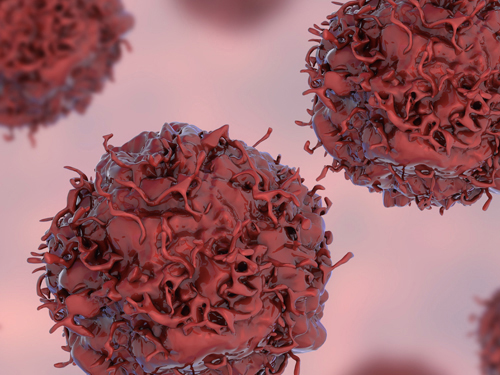 Early Genome Catastrophes Can Cause Non-Smoking Lung Cancer
Some teenagers harbor catastrophic changes to their genomes that can lead to lung cancer later on in life, even if they never smoke
(Professor Young Seok Ju at the Graduate School of Medical Science and Engineering)
Catastrophic rearrangements in the genome occurring as early as childhood and adolescence can lead to the development of lung cancer in later years in non-smokers. This finding, published in Cell, helps explain how some non-smoking-related lung cancers develop.
Researchers at KAIST, Seoul National University and their collaborators confirmed that gene fusions in non-smokers mostly occur early on, sometimes as early as childhood or adolescence, and on average about three decades before cancer is diagnosed. The study showed that these mutant lung cells, harboring oncogenic seeds, remain dormant for several decades until a number of further mutations accumulate sufficiently for progression into cancer. This is the first study to reveal the landscape of genome structural variations in lung adenocarcinoma.
Lung cancer is the leading cause of cancer-related deaths worldwide, and lung adenocarcinoma is its most common type. Most lung adenocarcinomas are associated with chronic smoking, but about a fourth develop in non-smokers. Precisely what happens in non-smokers for this cancer to develop is not clearly understood.
Researchers analyzed the genomes of 138 lung adenocarcinoma patients, including smokers and non-smokers, with whole-genome sequencing technologies. They explored DNA damage that induced neoplastic transformation.
Lung adenocarcinomas that originated from chronic smoking, referred to as signature 4-high (S4-high) cancers in the study, showed several distinguishing features compared to smoking-unrelated cancers (S4-low).
People in the S4-high group were largely older, men and had more frequent mutations in a cancer-related gene called KRAS. Cancer genomes in the S4-high group were hypermutated with simple mutational classes, such as the substitution, insertion, or deletion of a single base, the building block of DNA.
But the story was very different in the S4-low group. Generally, mutational profiles in this group were much more silent than the S4-high group. However, all cancer-related gene fusions, which are abnormally activated from the merging of two originally separate genes, were exclusively observed in the S4-low group.
The patterns of genomic structural changes underlying gene fusions suggest that about three in four cases of gene fusions emerged from a single cellular crisis causing massive genomic fragmentation and subsequent imprecise repair in normal lung epithelium.
Most strikingly, these major genomic rearrangements, which led to the development of lung adenocarcinoma, are very likely to be acquired decades before cancer diagnosis. The researchers used genomic archaeology techniques to trace the timing of when the catastrophes took place.
Researchers started this study seven years ago when they discovered the expression of the KIF5B-RET gene fusion in lung adenocarcinoma for the first time. Professor Young-Seok Ju, co-lead author from the Graduate School of Medical Science and Engineering at KAIST says, “It is remarkable that oncogenesis can begin by a massive shattering of chromosomes early in life. Our study immediately raises a new question: What induces the mutational catastrophe in our normal lung epithelium.”
Professor Young Tae Kim, co-lead author from Seoul National University says, “We hope this work will help us get one step closer to precision medicine for lung cancer patients.”
The research team plans to further focus on the molecular mechanisms that stimulate complex rearrangements in the body, through screening the genomic structures of fusion genes in other cancer types.
This study was supported by the National Research Foundation of Korea (NRF), Korea Health Industry Development Institute (KHIDI), Suh Kyungbae Foundation, the College of Medicine Research Foundations at Seoul National University and others.
Figure.
(Smoking-unrelated oncogenesis of lung cancers by gene fusions)
Publication.
Jake June-Koo Lee, Seongyeol Park et al., Tracing Oncogene Rearrangements in the Mutational History of Lung Adenocarcinoma
Cell 177, June 13 2019, online publication ahead of print at May 30, 2019
https://doi.org/10.1016/j.cell.2019.05.013
Profile: Prof Young Seok Ju, MD, PhD
ysju@kaist.ac.kr
http://julab.kaist.ac.kr
Associate Professor
Graduate School of Medical Science and Engineering (GSMSE)
Korea Advanced Institute of Science and Technology (KAIST)
Daejeon 34141, Korea
Profile: Prof Young Tae Kim, MD, PhD
ytkim@snu.ac.kr
Professor
Seoul National University Cancer Research Institute
Department of Thoracic and Cardiovascular Surgery
Seoul National University Hospital Seoul 03080, Korea
2019.05.31 View 58290
Early Genome Catastrophes Can Cause Non-Smoking Lung Cancer
Some teenagers harbor catastrophic changes to their genomes that can lead to lung cancer later on in life, even if they never smoke
(Professor Young Seok Ju at the Graduate School of Medical Science and Engineering)
Catastrophic rearrangements in the genome occurring as early as childhood and adolescence can lead to the development of lung cancer in later years in non-smokers. This finding, published in Cell, helps explain how some non-smoking-related lung cancers develop.
Researchers at KAIST, Seoul National University and their collaborators confirmed that gene fusions in non-smokers mostly occur early on, sometimes as early as childhood or adolescence, and on average about three decades before cancer is diagnosed. The study showed that these mutant lung cells, harboring oncogenic seeds, remain dormant for several decades until a number of further mutations accumulate sufficiently for progression into cancer. This is the first study to reveal the landscape of genome structural variations in lung adenocarcinoma.
Lung cancer is the leading cause of cancer-related deaths worldwide, and lung adenocarcinoma is its most common type. Most lung adenocarcinomas are associated with chronic smoking, but about a fourth develop in non-smokers. Precisely what happens in non-smokers for this cancer to develop is not clearly understood.
Researchers analyzed the genomes of 138 lung adenocarcinoma patients, including smokers and non-smokers, with whole-genome sequencing technologies. They explored DNA damage that induced neoplastic transformation.
Lung adenocarcinomas that originated from chronic smoking, referred to as signature 4-high (S4-high) cancers in the study, showed several distinguishing features compared to smoking-unrelated cancers (S4-low).
People in the S4-high group were largely older, men and had more frequent mutations in a cancer-related gene called KRAS. Cancer genomes in the S4-high group were hypermutated with simple mutational classes, such as the substitution, insertion, or deletion of a single base, the building block of DNA.
But the story was very different in the S4-low group. Generally, mutational profiles in this group were much more silent than the S4-high group. However, all cancer-related gene fusions, which are abnormally activated from the merging of two originally separate genes, were exclusively observed in the S4-low group.
The patterns of genomic structural changes underlying gene fusions suggest that about three in four cases of gene fusions emerged from a single cellular crisis causing massive genomic fragmentation and subsequent imprecise repair in normal lung epithelium.
Most strikingly, these major genomic rearrangements, which led to the development of lung adenocarcinoma, are very likely to be acquired decades before cancer diagnosis. The researchers used genomic archaeology techniques to trace the timing of when the catastrophes took place.
Researchers started this study seven years ago when they discovered the expression of the KIF5B-RET gene fusion in lung adenocarcinoma for the first time. Professor Young-Seok Ju, co-lead author from the Graduate School of Medical Science and Engineering at KAIST says, “It is remarkable that oncogenesis can begin by a massive shattering of chromosomes early in life. Our study immediately raises a new question: What induces the mutational catastrophe in our normal lung epithelium.”
Professor Young Tae Kim, co-lead author from Seoul National University says, “We hope this work will help us get one step closer to precision medicine for lung cancer patients.”
The research team plans to further focus on the molecular mechanisms that stimulate complex rearrangements in the body, through screening the genomic structures of fusion genes in other cancer types.
This study was supported by the National Research Foundation of Korea (NRF), Korea Health Industry Development Institute (KHIDI), Suh Kyungbae Foundation, the College of Medicine Research Foundations at Seoul National University and others.
Figure.
(Smoking-unrelated oncogenesis of lung cancers by gene fusions)
Publication.
Jake June-Koo Lee, Seongyeol Park et al., Tracing Oncogene Rearrangements in the Mutational History of Lung Adenocarcinoma
Cell 177, June 13 2019, online publication ahead of print at May 30, 2019
https://doi.org/10.1016/j.cell.2019.05.013
Profile: Prof Young Seok Ju, MD, PhD
ysju@kaist.ac.kr
http://julab.kaist.ac.kr
Associate Professor
Graduate School of Medical Science and Engineering (GSMSE)
Korea Advanced Institute of Science and Technology (KAIST)
Daejeon 34141, Korea
Profile: Prof Young Tae Kim, MD, PhD
ytkim@snu.ac.kr
Professor
Seoul National University Cancer Research Institute
Department of Thoracic and Cardiovascular Surgery
Seoul National University Hospital Seoul 03080, Korea
2019.05.31 View 58290 -
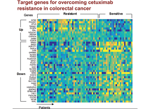 5 Biomarkers for Overcoming Colorectal Cancer Drug Resistance Identified
< Professor Kwang-Hyun Cho's Team >
KAIST researchers have identified five biomarkers that will help them address resistance to cancer-targeting therapeutics. This new treatment strategy will bring us one step closer to precision medicine for patients who showed resistance.
Colorectal cancer is one of the most common types of cancer worldwide. The number of patients has surpassed 1 million, and its five-year survival rate significantly drops to about 20 percent when metastasized. In Korea, the surge of colorectal cancer has been the highest in the last 10 years due to increasing Westernized dietary patterns and obesity. It is expected that the number and mortality rates of colorectal cancer patients will increase sharply as the nation is rapidly facing an increase in its aging population.
Recently, anticancer agents targeting only specific molecules of colon cancer cells have been developed. Unlike conventional anticancer medications, these selectively treat only specific target factors, so they can significantly reduce some of the side-effects of anticancer therapy while enhancing drug efficacy.
Cetuximab is the most well-known FDA approved anticancer medication. It is a biomarker that predicts drug reactivity and utilizes the presence of the ‘KRAS’ gene mutation. Cetuximab is prescribed to patients who don’t carry the KRAS gene mutation.
However, even in patients without the KRAS gene mutation, the response rate of Cetuximab is only about fifty percent, and there is also resistance to drugs after targeted chemotherapy. Compared with conventional chemotherapy alone, the life expectancy only lasts five months on average.
In research featured in the FEBS Journal as the cover paper for the April 7 edition, the KAIST research team led by Professor Kwang-Hyun Cho at the Department of Bio and Brain Engineering presented five additional biomarkers that could increase Cetuximab responsiveness using systems biology approach that combines genomic data analysis, mathematical modeling, and cell experiments. The experimental inhibition of newly discovered biomarkers DUSP4, ETV5, GNB5, NT5E, and PHLDA1 in colorectal cancer cells has been shown to overcome Cetuximab resistance in KRAS-normal genes. The research team confirmed that when suppressing GNB5, one of the new biomarkers, it was shown to overcome resistance to Cetuximab regardless of having a mutation in the KRAS gene.
Professor Cho said, “There has not been an example of colorectal cancer treatment involving regulation of the GNB5 gene.” He continued, “Identifying the principle of drug resistance in cancer cells through systems biology and discovering new biomarkers that could be a new molecular target to overcome drug resistance suggest real potential to actualize precision medicine.”
This study was supported by the National Research Foundation of Korea (NRF) and funded by the Ministry of Science and ICT (2017R1A2A1A17069642 and 2015M3A9A7067220).
Image 1. The cover of FEBS Journal for April 2019
2019.05.27 View 60853
5 Biomarkers for Overcoming Colorectal Cancer Drug Resistance Identified
< Professor Kwang-Hyun Cho's Team >
KAIST researchers have identified five biomarkers that will help them address resistance to cancer-targeting therapeutics. This new treatment strategy will bring us one step closer to precision medicine for patients who showed resistance.
Colorectal cancer is one of the most common types of cancer worldwide. The number of patients has surpassed 1 million, and its five-year survival rate significantly drops to about 20 percent when metastasized. In Korea, the surge of colorectal cancer has been the highest in the last 10 years due to increasing Westernized dietary patterns and obesity. It is expected that the number and mortality rates of colorectal cancer patients will increase sharply as the nation is rapidly facing an increase in its aging population.
Recently, anticancer agents targeting only specific molecules of colon cancer cells have been developed. Unlike conventional anticancer medications, these selectively treat only specific target factors, so they can significantly reduce some of the side-effects of anticancer therapy while enhancing drug efficacy.
Cetuximab is the most well-known FDA approved anticancer medication. It is a biomarker that predicts drug reactivity and utilizes the presence of the ‘KRAS’ gene mutation. Cetuximab is prescribed to patients who don’t carry the KRAS gene mutation.
However, even in patients without the KRAS gene mutation, the response rate of Cetuximab is only about fifty percent, and there is also resistance to drugs after targeted chemotherapy. Compared with conventional chemotherapy alone, the life expectancy only lasts five months on average.
In research featured in the FEBS Journal as the cover paper for the April 7 edition, the KAIST research team led by Professor Kwang-Hyun Cho at the Department of Bio and Brain Engineering presented five additional biomarkers that could increase Cetuximab responsiveness using systems biology approach that combines genomic data analysis, mathematical modeling, and cell experiments. The experimental inhibition of newly discovered biomarkers DUSP4, ETV5, GNB5, NT5E, and PHLDA1 in colorectal cancer cells has been shown to overcome Cetuximab resistance in KRAS-normal genes. The research team confirmed that when suppressing GNB5, one of the new biomarkers, it was shown to overcome resistance to Cetuximab regardless of having a mutation in the KRAS gene.
Professor Cho said, “There has not been an example of colorectal cancer treatment involving regulation of the GNB5 gene.” He continued, “Identifying the principle of drug resistance in cancer cells through systems biology and discovering new biomarkers that could be a new molecular target to overcome drug resistance suggest real potential to actualize precision medicine.”
This study was supported by the National Research Foundation of Korea (NRF) and funded by the Ministry of Science and ICT (2017R1A2A1A17069642 and 2015M3A9A7067220).
Image 1. The cover of FEBS Journal for April 2019
2019.05.27 View 60853 -
 Engineered Microbial Production of Grape Flavoring
(Image 1: Engineered bacteria that produce grape flavoring.)
Researchers report a microbial method for producing an artificial grape flavor. Methyl anthranilate (MANT) is a common grape flavoring and odorant compound currently produced through a petroleum-based process that uses large volumes of toxic acid catalysts.
Professor Sang-Yup Lee’s team at the Department of Chemical and Biomolecular Engineering demonstrated production of MANT, a naturally occurring compound, via engineered bacteria. The authors engineered strains of Escherichia coli and Corynebacetrium glutamicum to produce MANT through a plant-based engineered metabolic pathway.
The authors tuned the bacterial metabolic pathway by optimizing the levels of AAMT1, the key enzyme in the process. To maximize production of MANT, the authors tested six strategies, including increasing the supply of a precursor compound and enhancing the availability of a co-substrate. The most productive strategy proved to be a two-phase extractive culture, in which MANT was extracted into a solvent. This strategy produced MANT on the scale of 4.47 to 5.74 grams per liter, a significant amount, considering that engineered microbes produce most natural products at a scale of milligrams or micrograms per liter.
According to the authors, the results suggest that MANT and other related molecules produced through industrial processes can be produced at scale by engineered microbes in a manner that would allow them to be marketed as natural one, instead of artificial one.
This study, featured at the Proceeding of the National Academy of Sciences of the USA on May 13, was supported by the Technology Development Program to Solve Climate Changes on Systems Metabolic Engineering for Biorefineries from the Ministry of Science and ICT.
(Image 2. Overview of the strategies applied for the microbial production of grape flavoring.)
2019.05.15 View 57129
Engineered Microbial Production of Grape Flavoring
(Image 1: Engineered bacteria that produce grape flavoring.)
Researchers report a microbial method for producing an artificial grape flavor. Methyl anthranilate (MANT) is a common grape flavoring and odorant compound currently produced through a petroleum-based process that uses large volumes of toxic acid catalysts.
Professor Sang-Yup Lee’s team at the Department of Chemical and Biomolecular Engineering demonstrated production of MANT, a naturally occurring compound, via engineered bacteria. The authors engineered strains of Escherichia coli and Corynebacetrium glutamicum to produce MANT through a plant-based engineered metabolic pathway.
The authors tuned the bacterial metabolic pathway by optimizing the levels of AAMT1, the key enzyme in the process. To maximize production of MANT, the authors tested six strategies, including increasing the supply of a precursor compound and enhancing the availability of a co-substrate. The most productive strategy proved to be a two-phase extractive culture, in which MANT was extracted into a solvent. This strategy produced MANT on the scale of 4.47 to 5.74 grams per liter, a significant amount, considering that engineered microbes produce most natural products at a scale of milligrams or micrograms per liter.
According to the authors, the results suggest that MANT and other related molecules produced through industrial processes can be produced at scale by engineered microbes in a manner that would allow them to be marketed as natural one, instead of artificial one.
This study, featured at the Proceeding of the National Academy of Sciences of the USA on May 13, was supported by the Technology Development Program to Solve Climate Changes on Systems Metabolic Engineering for Biorefineries from the Ministry of Science and ICT.
(Image 2. Overview of the strategies applied for the microbial production of grape flavoring.)
2019.05.15 View 57129 -
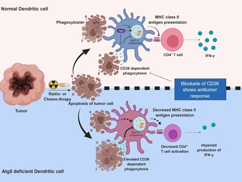 Autophagy in Dendritic Cells Helps Anticancer Activity
Autophagy contributes to the homeostasis of a cell and recently another function of autophagy has been reported. A KAIST research team found that the autophagy of dendritic cells supports T-cell anticancer activity.
Autophagy is a process of maintaining cell homeostasis by removing cellular waste and damaged cellular organelles; nevertheless, its role in the presentation of phagocytized tumor-associated antigens remains vague.
Meanwhile, dendritic cells are the ones that recognize pathogens or cancer antigens, and induce immune responses in T cells. When cancer cells are killed by radiation or an anticancer drug, dendritic cells absorb and remove them and present antigens on their surface to transfer them to T-cells.
Professor Heung Kyu Lee from the Graduate School of Medical Science and Engineering and his team found that the autophagy of dendritic cells plays a key role in T-cell activation and they proposed the principles of enhancing anti-cancer effects.
Their experiments showed that T-cell activation of dendritic cells as well as anticancer immune response dropped when there is a deficiency of Atg5 (autophagy-related) in dendritic cells.
Interestingly, Atg5-deficient dendritic cells significantly elevated receptor CD36 on the surface of the cells, which increased the phagocytosis of apoptotic tumor cells yet restricted the activation of T-cells.
At this time, when introducing antibodies into the system in order to block the receptor CD36, the anti-tumor T-cell response increased substantially while tumor growth declined.
Professor Lee said, “This study allowed us to explore the role of autophagy in the anti-cancer immune response of T-cells. We look forward to developing targeted anti-cancer therapies using the receptor CD36.”
This research was published in Autophagy (10.1080/15548627.2019.1596493) on March 22, 2019.
Figure 1.Mechanism of autophagy in dendritic cells
Figure 2. A role of autophagy in dendritic cells
2019.05.13 View 51879
Autophagy in Dendritic Cells Helps Anticancer Activity
Autophagy contributes to the homeostasis of a cell and recently another function of autophagy has been reported. A KAIST research team found that the autophagy of dendritic cells supports T-cell anticancer activity.
Autophagy is a process of maintaining cell homeostasis by removing cellular waste and damaged cellular organelles; nevertheless, its role in the presentation of phagocytized tumor-associated antigens remains vague.
Meanwhile, dendritic cells are the ones that recognize pathogens or cancer antigens, and induce immune responses in T cells. When cancer cells are killed by radiation or an anticancer drug, dendritic cells absorb and remove them and present antigens on their surface to transfer them to T-cells.
Professor Heung Kyu Lee from the Graduate School of Medical Science and Engineering and his team found that the autophagy of dendritic cells plays a key role in T-cell activation and they proposed the principles of enhancing anti-cancer effects.
Their experiments showed that T-cell activation of dendritic cells as well as anticancer immune response dropped when there is a deficiency of Atg5 (autophagy-related) in dendritic cells.
Interestingly, Atg5-deficient dendritic cells significantly elevated receptor CD36 on the surface of the cells, which increased the phagocytosis of apoptotic tumor cells yet restricted the activation of T-cells.
At this time, when introducing antibodies into the system in order to block the receptor CD36, the anti-tumor T-cell response increased substantially while tumor growth declined.
Professor Lee said, “This study allowed us to explore the role of autophagy in the anti-cancer immune response of T-cells. We look forward to developing targeted anti-cancer therapies using the receptor CD36.”
This research was published in Autophagy (10.1080/15548627.2019.1596493) on March 22, 2019.
Figure 1.Mechanism of autophagy in dendritic cells
Figure 2. A role of autophagy in dendritic cells
2019.05.13 View 51879 -
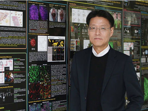 KAIST Identifies the Cause of Sepsis-induced Lung Injury
(Professor Pilhan Kim from the Graduate School of Medical Science and Engineering)
A KAIST research team succeeded in visualizing pulmonary microcirculation and circulating cells in vivo with a custom-built 3D intravital lung microscopic imaging system. They found a type of leukocyte called neutrophils aggregate inside the capillaries during sepsis-induced acute lung injury (ALI), leading to disturbances and dead space in blood microcirculation.
According to the researchers, this phenomenon is responsible for tissue hypoxia causing lung damage in the sepsis model, and mitigating neutrophils improves microcirculation as well as hypoxia.
The lungs are responsible for exchanging oxygen with carbon dioxide gases during the breathing process, providing an essential function for sustaining life. This gas exchange occurs in the alveoli, each surrounded by many capillaries containing the circulating red blood cells.
Researchers have been making efforts to observe microcirculation in alveoli, but it has been technically challenging to capture high-resolution images of capillaries and red blood cells inside the lungs that are in constant breathing motion.
Professor Pilhan Kim from the Graduate School of Medical Science and Engineering and his team developed an ultra-fast laser scanning confocal microscope and an imaging chamber that could minimize the movement of a lung while preserving its respiratory state. They used this technology to successfully capture red blood cell circulation inside the capillaries of animal models with sepsis.
During the process, they found that hypoxia was induced by the increase of dead space inside the lungs of a sepsis model, a space where red blood cells do not circulate. This phenomenon is due to the neutrophils aggregating and trapping inside the capillaries and the arterioles. It was also shown that trapped neutrophils damage the lung tissue in the sepsis model by inhibiting microcirculation as well as releasing reactive oxygen species.
Further studies showed that the aggregated neutrophils inside pulmonary vessels exhibit a higher expression of the Mac-1 receptor (CD11b/CD18), which is a receptor involved in intercellular adhesion, compared to the neutrophils that normally circulate. Additionally, they confirmed that Mac-1 inhibitors can improve inhibited microcirculation, ameliorate hypoxia, while reducing pulmonary edema in the sepsis model.
Their high-resolution 3D intravital microscope technology allows the real-time imaging of living cells inside the lungs. This work is expected to be used in research on various lung diseases, including sepsis.
The research team’s pulmonary circulation imaging and precise analytical techniques will be used as the base technology for developing new diagnostic technologies, evaluating new therapeutic agents for various diseases related to microcirculation.
Professor Kim said, “In the ALI model, the inhibition of pulmonary microcirculation occurs due to neutrophils. By controlling this effect and improving microcirculation, it is possible to eliminate hypoxia and pulmonary edema – a new, effective strategy for treating patients with sepsis.”
Their 3D intravital microscope technology was commercialized through IVIM Technology, Inc., which is a faculty startup at KAIST. They released an all-in-one intravital microscope model called ‘IVM-CM’ and ‘IVM-C’. This next-generation imaging equipment for basic biomedical research on the complex pathophysiology of various human diseases will play a crucial role in the future global bio-health market.
This research, led by Dr. Inwon Park from the Department of Emergency Medicine at Seoul National University Bundang Hospital and formally the Graduate School of Medical Science and Engineering at KAIST, was published in the European Respiratory Journal (2019, 53:1800736) on March 28, 2019.
Figure 1. Custom-built high-speed real-time intravital microscope platform
Figure 2. Illustrative schematic and photo of a 3D intravital lung microscopic imaging system
Figure 3. Aggregation of neutrophils and consequent flow disturbance in pulmonary arteriole in sepsis-induced lung injury
2019.05.07 View 45167
KAIST Identifies the Cause of Sepsis-induced Lung Injury
(Professor Pilhan Kim from the Graduate School of Medical Science and Engineering)
A KAIST research team succeeded in visualizing pulmonary microcirculation and circulating cells in vivo with a custom-built 3D intravital lung microscopic imaging system. They found a type of leukocyte called neutrophils aggregate inside the capillaries during sepsis-induced acute lung injury (ALI), leading to disturbances and dead space in blood microcirculation.
According to the researchers, this phenomenon is responsible for tissue hypoxia causing lung damage in the sepsis model, and mitigating neutrophils improves microcirculation as well as hypoxia.
The lungs are responsible for exchanging oxygen with carbon dioxide gases during the breathing process, providing an essential function for sustaining life. This gas exchange occurs in the alveoli, each surrounded by many capillaries containing the circulating red blood cells.
Researchers have been making efforts to observe microcirculation in alveoli, but it has been technically challenging to capture high-resolution images of capillaries and red blood cells inside the lungs that are in constant breathing motion.
Professor Pilhan Kim from the Graduate School of Medical Science and Engineering and his team developed an ultra-fast laser scanning confocal microscope and an imaging chamber that could minimize the movement of a lung while preserving its respiratory state. They used this technology to successfully capture red blood cell circulation inside the capillaries of animal models with sepsis.
During the process, they found that hypoxia was induced by the increase of dead space inside the lungs of a sepsis model, a space where red blood cells do not circulate. This phenomenon is due to the neutrophils aggregating and trapping inside the capillaries and the arterioles. It was also shown that trapped neutrophils damage the lung tissue in the sepsis model by inhibiting microcirculation as well as releasing reactive oxygen species.
Further studies showed that the aggregated neutrophils inside pulmonary vessels exhibit a higher expression of the Mac-1 receptor (CD11b/CD18), which is a receptor involved in intercellular adhesion, compared to the neutrophils that normally circulate. Additionally, they confirmed that Mac-1 inhibitors can improve inhibited microcirculation, ameliorate hypoxia, while reducing pulmonary edema in the sepsis model.
Their high-resolution 3D intravital microscope technology allows the real-time imaging of living cells inside the lungs. This work is expected to be used in research on various lung diseases, including sepsis.
The research team’s pulmonary circulation imaging and precise analytical techniques will be used as the base technology for developing new diagnostic technologies, evaluating new therapeutic agents for various diseases related to microcirculation.
Professor Kim said, “In the ALI model, the inhibition of pulmonary microcirculation occurs due to neutrophils. By controlling this effect and improving microcirculation, it is possible to eliminate hypoxia and pulmonary edema – a new, effective strategy for treating patients with sepsis.”
Their 3D intravital microscope technology was commercialized through IVIM Technology, Inc., which is a faculty startup at KAIST. They released an all-in-one intravital microscope model called ‘IVM-CM’ and ‘IVM-C’. This next-generation imaging equipment for basic biomedical research on the complex pathophysiology of various human diseases will play a crucial role in the future global bio-health market.
This research, led by Dr. Inwon Park from the Department of Emergency Medicine at Seoul National University Bundang Hospital and formally the Graduate School of Medical Science and Engineering at KAIST, was published in the European Respiratory Journal (2019, 53:1800736) on March 28, 2019.
Figure 1. Custom-built high-speed real-time intravital microscope platform
Figure 2. Illustrative schematic and photo of a 3D intravital lung microscopic imaging system
Figure 3. Aggregation of neutrophils and consequent flow disturbance in pulmonary arteriole in sepsis-induced lung injury
2019.05.07 View 45167 -
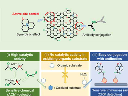 Nanomaterials Mimicking Natural Enzymes with Superior Catalytic Activity and Selectivity for Detecting Acetylcholine
(Professor Jinwoo Lee from the Department of Chemical and Biomolecular Engineering)
A KAIST research team doped nitrogen and boron into graphene to selectively increase peroxidase-like activity and succeeded in synthesizing a peroxidase-mimicking nanozyme with a low cost and superior catalytic activity. These nanomaterials can be applied for early diagnosis of Alzheimer’s disease.
Enzymes are the main catalysts in our body and are widely used in bioassays. In particular, peroxidase, which oxidizes transparent colorimetric substrates to become a colored product in the presence of hydrogen peroxide, is the most common enzyme that is used in colorimetric bioassays.
However, natural enzymes consisting of proteins are unstable against temperature and pH, hard to synthesize, and costly. Nanozymes, on the other hand, do not consist of proteins, meaning the disadvantages of enzymes can be overcome with their robustness and high productivity. In contrast, most nanonzymes do not have selectivity; for example, peroxidase-mimicking nanozymes demonstrate oxidase-like activity that oxidizes colorimetric substrates in the absence of hydrogen peroxide, which keeps them away from precisely detecting the target materials, such as hydrogen peroxide.
Professor Jinwoo Lee from the Department of Chemical and Biomolecular Engineering and his team were able to synthesize a peroxidase-mimicking nanozyme with superior catalytic activity and selectivity toward hydrogen peroxide. Co-doping of nitrogen and boron into graphene, which has negligible peroxidase-like activity, selectively increased the peroxidase-like activity without oxidase-like activity to accurately mimic the nature peroxidase and has become a powerful candidate to replace the peroxidase.
The experimental results were also verified with computational chemistry. The nitrogen and boron co-doped graphene was also applied to the colorimetric detection of acetylcholine, which is an important neurotransmitter and successfully detected the acetylcholine even better than the nature peroxidase.
Professor Lee said, “We began to study nanozymes due to their potential for replacing existing enzymes. Through this study, we have secured core technologies to synthesize nanozymes that have high enzyme activity along with selectivity. We believe that they can be applied to effectively detect acetylcholine for quickly diagnosing Alzheimer’s disease.
This research, led by PhD Min Su Kim, was published in ACS Nano (10.1021/acsnano.8b09519) on March 25, 2019.
Figure 1. Comparison of the catalytic activities of various nanozymes and horseradish peroxidase (HRP) toward TMB and H₂O₂
Figure 2. Schematic illustration of NB-rGO Reactions in Bioassays
2019.04.30 View 38322
Nanomaterials Mimicking Natural Enzymes with Superior Catalytic Activity and Selectivity for Detecting Acetylcholine
(Professor Jinwoo Lee from the Department of Chemical and Biomolecular Engineering)
A KAIST research team doped nitrogen and boron into graphene to selectively increase peroxidase-like activity and succeeded in synthesizing a peroxidase-mimicking nanozyme with a low cost and superior catalytic activity. These nanomaterials can be applied for early diagnosis of Alzheimer’s disease.
Enzymes are the main catalysts in our body and are widely used in bioassays. In particular, peroxidase, which oxidizes transparent colorimetric substrates to become a colored product in the presence of hydrogen peroxide, is the most common enzyme that is used in colorimetric bioassays.
However, natural enzymes consisting of proteins are unstable against temperature and pH, hard to synthesize, and costly. Nanozymes, on the other hand, do not consist of proteins, meaning the disadvantages of enzymes can be overcome with their robustness and high productivity. In contrast, most nanonzymes do not have selectivity; for example, peroxidase-mimicking nanozymes demonstrate oxidase-like activity that oxidizes colorimetric substrates in the absence of hydrogen peroxide, which keeps them away from precisely detecting the target materials, such as hydrogen peroxide.
Professor Jinwoo Lee from the Department of Chemical and Biomolecular Engineering and his team were able to synthesize a peroxidase-mimicking nanozyme with superior catalytic activity and selectivity toward hydrogen peroxide. Co-doping of nitrogen and boron into graphene, which has negligible peroxidase-like activity, selectively increased the peroxidase-like activity without oxidase-like activity to accurately mimic the nature peroxidase and has become a powerful candidate to replace the peroxidase.
The experimental results were also verified with computational chemistry. The nitrogen and boron co-doped graphene was also applied to the colorimetric detection of acetylcholine, which is an important neurotransmitter and successfully detected the acetylcholine even better than the nature peroxidase.
Professor Lee said, “We began to study nanozymes due to their potential for replacing existing enzymes. Through this study, we have secured core technologies to synthesize nanozymes that have high enzyme activity along with selectivity. We believe that they can be applied to effectively detect acetylcholine for quickly diagnosing Alzheimer’s disease.
This research, led by PhD Min Su Kim, was published in ACS Nano (10.1021/acsnano.8b09519) on March 25, 2019.
Figure 1. Comparison of the catalytic activities of various nanozymes and horseradish peroxidase (HRP) toward TMB and H₂O₂
Figure 2. Schematic illustration of NB-rGO Reactions in Bioassays
2019.04.30 View 38322 -
 KAIST Unveils the Hidden Control Architecture of Brain Networks
(Professor Kwang-Hyun Cho and his team)
A KAIST research team identified the intrinsic control architecture of brain networks. The control properties will contribute to providing a fundamental basis for the exogenous control of brain networks and, therefore, has broad implications in cognitive and clinical neuroscience.
Although efficiency and robustness are often regarded as having a trade-off relationship, the human brain usually exhibits both attributes when it performs complex cognitive functions. Such optimality must be rooted in a specific coordinated control of interconnected brain regions, but the understanding of the intrinsic control architecture of brain networks is lacking.
Professor Kwang-Hyun Cho from the Department of Bio and Brain Engineering and his team investigated the intrinsic control architecture of brain networks. They employed an interdisciplinary approach that spans connectomics, neuroscience, control engineering, network science, and systems biology to examine the structural brain networks of various species and compared them with the control architecture of other biological networks, as well as man-made ones, such as social, infrastructural and technological networks.
In particular, the team reconstructed the structural brain networks of 100 healthy human adults by performing brain parcellation and tractography with structural and diffusion imaging data obtained from the Human Connectome Project database of the US National Institutes of Health.
The team developed a framework for analyzing the control architecture of brain networks based on the minimum dominating set (MDSet), which refers to a minimal subset of nodes (MD-nodes) that control the remaining nodes with a one-step direct interaction. MD-nodes play a crucial role in various complex networks including biomolecular networks, but they have not been investigated in brain networks.
By exploring and comparing the structural principles underlying the composition of MDSets of various complex networks, the team delineated their distinct control architectures. Interestingly, the team found that the proportion of MDSets in brain networks is remarkably small compared to those of other complex networks. This finding implies that brain networks may have been optimized for minimizing the cost required for controlling networks. Furthermore, the team found that the MDSets of brain networks are not solely determined by the degree of nodes, but rather strategically placed to form a particular control architecture.
Consequently, the team revealed the hidden control architecture of brain networks, namely, the distributed and overlapping control architecture that is distinct from other complex networks. The team found that such a particular control architecture brings about robustness against targeted attacks (i.e., preferential attacks on high-degree nodes) which might be a fundamental basis of robust brain functions against preferential damage of high-degree nodes (i.e., brain regions).
Moreover, the team found that the particular control architecture of brain networks also enables high efficiency in switching from one network state, defined by a set of node activities, to another – a capability that is crucial for traversing diverse cognitive states.
Professor Cho said, “This study is the first attempt to make a quantitative comparison between brain networks and other real-world complex networks. Understanding of intrinsic control architecture underlying brain networks may enable the development of optimal interventions for therapeutic purposes or cognitive enhancement.”
This research, led by Byeongwook Lee, Uiryong Kang and Hongjun Chang, was published in iScience (10.1016/j.isci.2019.02.017) on March 29, 2019.
Figure 1. Schematic of identification of control architecture of brain networks.
Figure 2. Identified control architectures of brain networks and other real-world complex networks.
2019.04.23 View 39050
KAIST Unveils the Hidden Control Architecture of Brain Networks
(Professor Kwang-Hyun Cho and his team)
A KAIST research team identified the intrinsic control architecture of brain networks. The control properties will contribute to providing a fundamental basis for the exogenous control of brain networks and, therefore, has broad implications in cognitive and clinical neuroscience.
Although efficiency and robustness are often regarded as having a trade-off relationship, the human brain usually exhibits both attributes when it performs complex cognitive functions. Such optimality must be rooted in a specific coordinated control of interconnected brain regions, but the understanding of the intrinsic control architecture of brain networks is lacking.
Professor Kwang-Hyun Cho from the Department of Bio and Brain Engineering and his team investigated the intrinsic control architecture of brain networks. They employed an interdisciplinary approach that spans connectomics, neuroscience, control engineering, network science, and systems biology to examine the structural brain networks of various species and compared them with the control architecture of other biological networks, as well as man-made ones, such as social, infrastructural and technological networks.
In particular, the team reconstructed the structural brain networks of 100 healthy human adults by performing brain parcellation and tractography with structural and diffusion imaging data obtained from the Human Connectome Project database of the US National Institutes of Health.
The team developed a framework for analyzing the control architecture of brain networks based on the minimum dominating set (MDSet), which refers to a minimal subset of nodes (MD-nodes) that control the remaining nodes with a one-step direct interaction. MD-nodes play a crucial role in various complex networks including biomolecular networks, but they have not been investigated in brain networks.
By exploring and comparing the structural principles underlying the composition of MDSets of various complex networks, the team delineated their distinct control architectures. Interestingly, the team found that the proportion of MDSets in brain networks is remarkably small compared to those of other complex networks. This finding implies that brain networks may have been optimized for minimizing the cost required for controlling networks. Furthermore, the team found that the MDSets of brain networks are not solely determined by the degree of nodes, but rather strategically placed to form a particular control architecture.
Consequently, the team revealed the hidden control architecture of brain networks, namely, the distributed and overlapping control architecture that is distinct from other complex networks. The team found that such a particular control architecture brings about robustness against targeted attacks (i.e., preferential attacks on high-degree nodes) which might be a fundamental basis of robust brain functions against preferential damage of high-degree nodes (i.e., brain regions).
Moreover, the team found that the particular control architecture of brain networks also enables high efficiency in switching from one network state, defined by a set of node activities, to another – a capability that is crucial for traversing diverse cognitive states.
Professor Cho said, “This study is the first attempt to make a quantitative comparison between brain networks and other real-world complex networks. Understanding of intrinsic control architecture underlying brain networks may enable the development of optimal interventions for therapeutic purposes or cognitive enhancement.”
This research, led by Byeongwook Lee, Uiryong Kang and Hongjun Chang, was published in iScience (10.1016/j.isci.2019.02.017) on March 29, 2019.
Figure 1. Schematic of identification of control architecture of brain networks.
Figure 2. Identified control architectures of brain networks and other real-world complex networks.
2019.04.23 View 39050 -
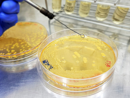
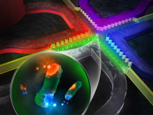 On-chip Drug Screening for Identifying Antibiotic Interactions in Eight Hours
(from left: Seunggyu Kimand Professor Jessie Sungyun Jeon)
A KAIST research team developed a microfluidic-based drug screening chip that identifies synergistic interactions between two antibiotics in eight hours. This chip can be a cell-based drug screening platform for exploring critical pharmacological patterns of antibiotic interactions, along with potential applications in screening other cell-type agents and guidance for clinical therapies.
Antibiotic susceptibility testing, which determines types and doses of antibiotics that can effectively inhibit bacterial growth, has become more critical in recent years with the emergence of antibiotic-resistant pathogenic bacteria strains.
To overcome the antibiotic-resistant bacteria, combinatory therapy using two or more kinds of antibiotics has been gaining considerable attention. However, the major problem is that this therapy is not always effective; occasionally, unfavorable antibiotic pairs may worsen results, leading to suppressed antimicrobial effects. Therefore, combinatory testing is a crucial preliminary process to find suitable antibiotic pairs and their concentration range against unknown pathogens, but the conventional testing methods are inconvenient for concentration dilution and sample preparation, and they take more than 24 hours to produce the results.
To reduce time and enhance the efficiency of combinatory testing, Professor Jessie Sungyun Jeon from the Department of Mechanical Engineering, in collaboration with Professor Hyun Jung Chung from the Department of Biological Sciences, developed a high-throughput drug screening chip that generates 121 pairwise concentrations between two antibiotics.
The team utilized a microfluidic chip with a sample volume of a few tens of microliters. This chip enabled 121 pairwise concentrations of two antibiotics to be automatically formed in only 35 minutes.
They loaded a mixture of bacterial samples and agarose into the microchannel and injected reagents with or without antibiotics into the surrounding microchannel. The diffusion of antibiotic molecules from the channel with antibiotics to the one without antibiotics resulted in the formation of two orthogonal concentration gradients of the two antibiotics on the bacteria-trapping agarose gel.
The team observed the inhibition of bacterial growth by the antibiotic orthogonal gradients over six hours with a microscope, and confirmed different patterns of antibiotic pairs, classifying the interaction types into either synergy or antagonism.
Professor Jeon said, “The feasibility of microfluidic-based drug screening chips is promising, and we expect our microfluidic chip to be commercialized and utilized in near future.”
This study, led by Seunggyu Kim, was published in Lab on a Chip (10.1039/c8lc01406j) on March 21, 2019.
Figure 1. Back cover image for the “Lab on a Chip”.
Figure 2. Examples of testing results using the microfluidic chips developed in this research.
2019.04.18 View 31869
On-chip Drug Screening for Identifying Antibiotic Interactions in Eight Hours
(from left: Seunggyu Kimand Professor Jessie Sungyun Jeon)
A KAIST research team developed a microfluidic-based drug screening chip that identifies synergistic interactions between two antibiotics in eight hours. This chip can be a cell-based drug screening platform for exploring critical pharmacological patterns of antibiotic interactions, along with potential applications in screening other cell-type agents and guidance for clinical therapies.
Antibiotic susceptibility testing, which determines types and doses of antibiotics that can effectively inhibit bacterial growth, has become more critical in recent years with the emergence of antibiotic-resistant pathogenic bacteria strains.
To overcome the antibiotic-resistant bacteria, combinatory therapy using two or more kinds of antibiotics has been gaining considerable attention. However, the major problem is that this therapy is not always effective; occasionally, unfavorable antibiotic pairs may worsen results, leading to suppressed antimicrobial effects. Therefore, combinatory testing is a crucial preliminary process to find suitable antibiotic pairs and their concentration range against unknown pathogens, but the conventional testing methods are inconvenient for concentration dilution and sample preparation, and they take more than 24 hours to produce the results.
To reduce time and enhance the efficiency of combinatory testing, Professor Jessie Sungyun Jeon from the Department of Mechanical Engineering, in collaboration with Professor Hyun Jung Chung from the Department of Biological Sciences, developed a high-throughput drug screening chip that generates 121 pairwise concentrations between two antibiotics.
The team utilized a microfluidic chip with a sample volume of a few tens of microliters. This chip enabled 121 pairwise concentrations of two antibiotics to be automatically formed in only 35 minutes.
They loaded a mixture of bacterial samples and agarose into the microchannel and injected reagents with or without antibiotics into the surrounding microchannel. The diffusion of antibiotic molecules from the channel with antibiotics to the one without antibiotics resulted in the formation of two orthogonal concentration gradients of the two antibiotics on the bacteria-trapping agarose gel.
The team observed the inhibition of bacterial growth by the antibiotic orthogonal gradients over six hours with a microscope, and confirmed different patterns of antibiotic pairs, classifying the interaction types into either synergy or antagonism.
Professor Jeon said, “The feasibility of microfluidic-based drug screening chips is promising, and we expect our microfluidic chip to be commercialized and utilized in near future.”
This study, led by Seunggyu Kim, was published in Lab on a Chip (10.1039/c8lc01406j) on March 21, 2019.
Figure 1. Back cover image for the “Lab on a Chip”.
Figure 2. Examples of testing results using the microfluidic chips developed in this research.
2019.04.18 View 31869 -
 A Hole in One for Holographic Display
(Professor YongKeun Park)
Researchers have designed an ultrathin display that can project dynamic, multi-coloured, 3D holographic images, according to a study published in Nature Communications.
The system’s critical component is a thin film of titanium filled with tiny holes that precisely correspond with each pixel in a liquid crystal display (LCD) panel. This film acts as a ‘photon sieve’ – each pinhole diffracts light emerging from them widely, resulting in a high-definition 3D image observable from a wide angle.
The entire system is very small: they used a 1.8-inch off-the-shelf LCD panel with a resolution of 1024 x 768. The titanium film, attached to the back of the panel, is a mere 300 nanometres thick.
“Our approach suggests that holographic displays could be projected from thin devices, like a cell phone,” says Professor YongKeun Park, a physicist at KAIST who led the research. The team demonstrated their approach by producing a hologram of a moving, tri-coloured cube.
Specifically, the images are made by pointing differently coloured laser beams made of parallel light rays at the small LCD panel. The photon sieve has a hole for each pixel in the LCD panel. The holes are precisely positioned to correspond to the pixel’s active area. The pinholes diffract the light emerging from them, producing 3D images.
Previous studies from Professor Park’s group have used optical diffusors for the same purpose, but the size of the device was bulky and difficult to be operated, and it took a long period of time to calibrate. In the present work, on the other hand, the group tailored their photon sieve to demonstrate a simple, compact and scalable method for 3D holographic display. This technique can be readily applied to existing LCD displays.
Applications for holograms have been limited by cumbersome techniques, high computation requirements, and poor image quality. Improving current techniques could lead to a wide variety of applications, including 3D cinema viewing without the need for glasses, watching holographic videos on television and smart phone screens.
Figure 1. The actual 3D holographic display, and an electron microscope image of the non-periodic pinholes.
Figure 2. Three-dimensional dynamic color hologram operating at 60 Hz
2019.04.18 View 33526
A Hole in One for Holographic Display
(Professor YongKeun Park)
Researchers have designed an ultrathin display that can project dynamic, multi-coloured, 3D holographic images, according to a study published in Nature Communications.
The system’s critical component is a thin film of titanium filled with tiny holes that precisely correspond with each pixel in a liquid crystal display (LCD) panel. This film acts as a ‘photon sieve’ – each pinhole diffracts light emerging from them widely, resulting in a high-definition 3D image observable from a wide angle.
The entire system is very small: they used a 1.8-inch off-the-shelf LCD panel with a resolution of 1024 x 768. The titanium film, attached to the back of the panel, is a mere 300 nanometres thick.
“Our approach suggests that holographic displays could be projected from thin devices, like a cell phone,” says Professor YongKeun Park, a physicist at KAIST who led the research. The team demonstrated their approach by producing a hologram of a moving, tri-coloured cube.
Specifically, the images are made by pointing differently coloured laser beams made of parallel light rays at the small LCD panel. The photon sieve has a hole for each pixel in the LCD panel. The holes are precisely positioned to correspond to the pixel’s active area. The pinholes diffract the light emerging from them, producing 3D images.
Previous studies from Professor Park’s group have used optical diffusors for the same purpose, but the size of the device was bulky and difficult to be operated, and it took a long period of time to calibrate. In the present work, on the other hand, the group tailored their photon sieve to demonstrate a simple, compact and scalable method for 3D holographic display. This technique can be readily applied to existing LCD displays.
Applications for holograms have been limited by cumbersome techniques, high computation requirements, and poor image quality. Improving current techniques could lead to a wide variety of applications, including 3D cinema viewing without the need for glasses, watching holographic videos on television and smart phone screens.
Figure 1. The actual 3D holographic display, and an electron microscope image of the non-periodic pinholes.
Figure 2. Three-dimensional dynamic color hologram operating at 60 Hz
2019.04.18 View 33526 -
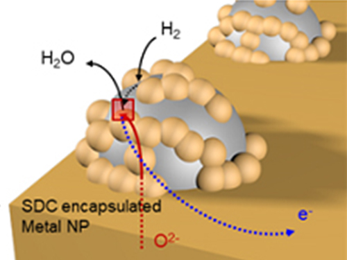 Unravelling Inherent Electrocatalysis to Improve the Performance of Hydrogen Fuel Cells
(Figure 1. Electrode structure for the precise evaluation of the metal nanoparticles’ electrochemical catalytic characteristics at a high temperature.)
A KAIST team presented an ideal electrode design to enhance the performance of high-temperature fuel cells. The new analytical platform with advanced nanoscale patterning method quantitatively revealed the electrochemical value of metal nanoparticles dispersed on the oxide electrode, thus leading to electrode design directions that can be used in a variety of eco-friendly energy technologies.
The team, working under Professor WooChul Jung and Professor Sang Ouk Kim at the Department of Materials Science and Engineering, described an accurate analysis of the reactivity of oxide electrodes boosted by metal nanoparticles, where all particles participate in the reaction. They identified how the metal catalysts activate hydrogen electro-oxidation on the ceria-based electrode surface and quantify how rapidly the reaction rate increases with the proper choice of metals.
Metal nanoparticles with diameters of 10 nanometers or less have become a key component in high-performance heterogeneous catalysts, primarily serving as a catalytic activator. Recent experimental and theoretical findings suggest that the optimization of the chemical nature at the metal and support interfaces is essential for performance improvement.
However, the high cost associated with cell fabrication and operation as well as poorer stability of metal nanoparticles at high temperatures have been a long-standing challenge. To solve this problem, the team utilized a globally recognized metal nano patterning technology that uses block copolymer self-assembled nano templates and succeeded in uniformly synthesizing metal particles 10 nanometers in size on the surface of oxide fuel cell electrodes. They also developed a technology to accurately analyze the catalyst characteristics of single particles at high temperatures and maximize the performance of a fuel cell with minimal catalyst use.
The research team confirmed that platinum, which is a commonly used metal catalyst, could boost fuel cell performance by as much as 21 times even at an amount of 300 nanograms, which only costs about 0.015 KRW.
The team quantitatively identified and compared the characteristics of widely used metal catalysts other than platinum, such as palladium, gold, and cobalt, and also elucidated the precise principle of catalyst performance through theoretical analysis.
(Figure 2. Comparison of the electrochemical catalytic characteristics for various 10nm metal nanoparticles (platinum, palladium, cobalt, gold) at a high temperature.)
Professor Jung said, "We have broken the conventional methods of increasing the amount of catalyst which have deemed inefficient and expensive. Our results suggest a clear idea for high performance fuel cells using very small amounts of nanoparticles. This technology can be applied to many different industrial fields, advancing the commercialization of eco-friendly energy technologies such as fuel cells that generate electricity and electrolytic cells that produce hydrogen from water.”
The research has been published as the cover article of Nature Nanotechnology in the March issue. This research was carried out with support from the Nano-Material Technology Development Program through the National Research Foundation of Korea.
2019.03.28 View 31120
Unravelling Inherent Electrocatalysis to Improve the Performance of Hydrogen Fuel Cells
(Figure 1. Electrode structure for the precise evaluation of the metal nanoparticles’ electrochemical catalytic characteristics at a high temperature.)
A KAIST team presented an ideal electrode design to enhance the performance of high-temperature fuel cells. The new analytical platform with advanced nanoscale patterning method quantitatively revealed the electrochemical value of metal nanoparticles dispersed on the oxide electrode, thus leading to electrode design directions that can be used in a variety of eco-friendly energy technologies.
The team, working under Professor WooChul Jung and Professor Sang Ouk Kim at the Department of Materials Science and Engineering, described an accurate analysis of the reactivity of oxide electrodes boosted by metal nanoparticles, where all particles participate in the reaction. They identified how the metal catalysts activate hydrogen electro-oxidation on the ceria-based electrode surface and quantify how rapidly the reaction rate increases with the proper choice of metals.
Metal nanoparticles with diameters of 10 nanometers or less have become a key component in high-performance heterogeneous catalysts, primarily serving as a catalytic activator. Recent experimental and theoretical findings suggest that the optimization of the chemical nature at the metal and support interfaces is essential for performance improvement.
However, the high cost associated with cell fabrication and operation as well as poorer stability of metal nanoparticles at high temperatures have been a long-standing challenge. To solve this problem, the team utilized a globally recognized metal nano patterning technology that uses block copolymer self-assembled nano templates and succeeded in uniformly synthesizing metal particles 10 nanometers in size on the surface of oxide fuel cell electrodes. They also developed a technology to accurately analyze the catalyst characteristics of single particles at high temperatures and maximize the performance of a fuel cell with minimal catalyst use.
The research team confirmed that platinum, which is a commonly used metal catalyst, could boost fuel cell performance by as much as 21 times even at an amount of 300 nanograms, which only costs about 0.015 KRW.
The team quantitatively identified and compared the characteristics of widely used metal catalysts other than platinum, such as palladium, gold, and cobalt, and also elucidated the precise principle of catalyst performance through theoretical analysis.
(Figure 2. Comparison of the electrochemical catalytic characteristics for various 10nm metal nanoparticles (platinum, palladium, cobalt, gold) at a high temperature.)
Professor Jung said, "We have broken the conventional methods of increasing the amount of catalyst which have deemed inefficient and expensive. Our results suggest a clear idea for high performance fuel cells using very small amounts of nanoparticles. This technology can be applied to many different industrial fields, advancing the commercialization of eco-friendly energy technologies such as fuel cells that generate electricity and electrolytic cells that produce hydrogen from water.”
The research has been published as the cover article of Nature Nanotechnology in the March issue. This research was carried out with support from the Nano-Material Technology Development Program through the National Research Foundation of Korea.
2019.03.28 View 31120 -
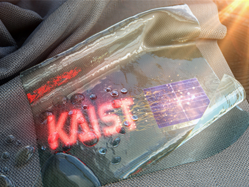 True-meaning Wearable Displays: Self-powered, Washable and Wearable
(Video: The washing process of wearing display module) When we think about clothes, they are usually formed with textiles and have to be both wearable and washable for daily use; however, smart clothing has had a problem with its power sources and moisture permeability, which causes the devices to malfunction. This problem has now been overcome by a KAIST research team, who developed a textile-based wearable display module technology that is washable and does not require an external power source.
To ease out the problem of external power sources and enhance the practicability of wearable displays, Professor Kyung Cheol Choi from the School of Electrical Engineering and his team fabricated their wearing display modules on real textiles that integrated polymer solar cells (PSCs) with organic light emitting diodes (OLEDs).
PSCs have been one of the most promising candidates for a next-generation power source, especially for wearable and optoelectronic applications because they can provide stable power without an external power source, while OLEDs can be driven with milliwatts. However, the problem was that they are both very vulnerable to external moisture and oxygen. The encapsulation barrier is essential for their reliability. The conventional encapsulation barrier is sufficient for normal environments; however, it loses its characteristics in aqueous environments, such as water. It limits the commercialization of wearing displays that must operate even on rainy days or after washing.
To tackle this issue, the team employed a washable encapsulation barrier that can protect the device without losing its characteristics after washing through atomic layer deposition (ALD) and spin coating. With this encapsulation technology, the team confirmed that textile-based wearing display modules including PSCs, OLEDs, and the proposed encapsulation barrier exhibited little change in characteristics even after 20 washings with 10-minute cycles. Moreover, the encapsulated device operated stably with a low curvature radius of 3mm and boasted high reliability.
Finally, it exhibited no deterioration in properties over 30 days even after being subjected to both bending stress and washing. Since it uses a less stressful textile, compared to conventional wearable electronic devices that use traditional plastic substrates, this technology can accelerate the commercialization of wearing electronic devices. Importantly, this wearable electronic device in daily life can save energy through a self-powered system.
Professor Choi said, “I could say that this research realized a truly washable wearable electronic module in the sense that it uses daily wearable textiles instead of the plastic used in conventional wearable electronic devices. Saving energy with PSCs, it can be self-powered, using nature-friendly solar energy, and washed. I believe that it has paved the way for a ‘true-meaning wearable display’ that can be formed on textile, beyond the attachable form of wearable technology.”
This research, in collaboration with Professor Seok Ho Cho from Chonnam National University and led by Eun Gyo Jeong, was published in Energy and Environmental Science (10.1039/c8ee03271h) on January 18, 2019.
Figure 1. Schematic and photo of a washable wearing display module
Figure 2. Cover page of Energy and Environmental Science
2019.03.21 View 32082
True-meaning Wearable Displays: Self-powered, Washable and Wearable
(Video: The washing process of wearing display module) When we think about clothes, they are usually formed with textiles and have to be both wearable and washable for daily use; however, smart clothing has had a problem with its power sources and moisture permeability, which causes the devices to malfunction. This problem has now been overcome by a KAIST research team, who developed a textile-based wearable display module technology that is washable and does not require an external power source.
To ease out the problem of external power sources and enhance the practicability of wearable displays, Professor Kyung Cheol Choi from the School of Electrical Engineering and his team fabricated their wearing display modules on real textiles that integrated polymer solar cells (PSCs) with organic light emitting diodes (OLEDs).
PSCs have been one of the most promising candidates for a next-generation power source, especially for wearable and optoelectronic applications because they can provide stable power without an external power source, while OLEDs can be driven with milliwatts. However, the problem was that they are both very vulnerable to external moisture and oxygen. The encapsulation barrier is essential for their reliability. The conventional encapsulation barrier is sufficient for normal environments; however, it loses its characteristics in aqueous environments, such as water. It limits the commercialization of wearing displays that must operate even on rainy days or after washing.
To tackle this issue, the team employed a washable encapsulation barrier that can protect the device without losing its characteristics after washing through atomic layer deposition (ALD) and spin coating. With this encapsulation technology, the team confirmed that textile-based wearing display modules including PSCs, OLEDs, and the proposed encapsulation barrier exhibited little change in characteristics even after 20 washings with 10-minute cycles. Moreover, the encapsulated device operated stably with a low curvature radius of 3mm and boasted high reliability.
Finally, it exhibited no deterioration in properties over 30 days even after being subjected to both bending stress and washing. Since it uses a less stressful textile, compared to conventional wearable electronic devices that use traditional plastic substrates, this technology can accelerate the commercialization of wearing electronic devices. Importantly, this wearable electronic device in daily life can save energy through a self-powered system.
Professor Choi said, “I could say that this research realized a truly washable wearable electronic module in the sense that it uses daily wearable textiles instead of the plastic used in conventional wearable electronic devices. Saving energy with PSCs, it can be self-powered, using nature-friendly solar energy, and washed. I believe that it has paved the way for a ‘true-meaning wearable display’ that can be formed on textile, beyond the attachable form of wearable technology.”
This research, in collaboration with Professor Seok Ho Cho from Chonnam National University and led by Eun Gyo Jeong, was published in Energy and Environmental Science (10.1039/c8ee03271h) on January 18, 2019.
Figure 1. Schematic and photo of a washable wearing display module
Figure 2. Cover page of Energy and Environmental Science
2019.03.21 View 32082 -
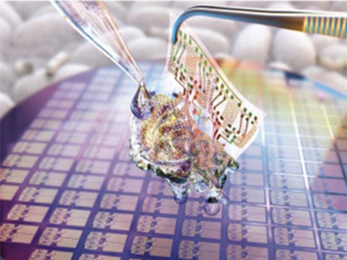 Wafer-Scale Multilayer Fabrication of Silk Fibroin-Based Microelectronics
A KAIST research team developed a novel fabrication method for the multilayer processing of silk-based microelectronics. This technology for creating a biodegradable silk fibroin film allows microfabrication with polymer or metal structures manufactured from photolithography. It can be a key technology in the implementation of silk fibroin-based biodegradable electronic devices or localized drug delivery through silk fibroin patterns.
Silk fibroins are biocompatible, biodegradable, transparent, and flexible, which makes them excellent candidates for implantable biomedical devices, and they have also been used as biodegradable films and functional microstructures in biomedical applications. However, conventional microfabrication processes require strong etching solutions and solvents to modify the structure of silk fibroins.
To prevent the silk fibroin from being damaged during the process, Professor Hyunjoo J. Lee from the School of Electrical Engineering and her team came up with a novel process, named aluminum hard mask on silk fibroin (AMoS), which is capable of micropatterning multiple layers composed of both fibroin and inorganic materials, such as metal and dielectrics with high-precision microscale alignment. The AMoS process can make silk fibroin patterns on devices, or make patterns on silk fibroin thin films with other materials by using photolithography, which is a core technology in the current microfabrication process.
The team successfully cultured primary neurons on the processed silk fibroin micro-patterns, and confirmed that silk fibroin has excellent biocompatibility before and after the fabrication process and that it also can be applied to implanted biological devices.
Through this technology, the team realized the multilayer micropatterning of fibroin films on a silk fibroin substrate and fabricated a biodegradable microelectric circuit consisting of resistors and silk fibroin dielectric capacitors in a silicon wafer with large areas.
They also used this technology to position the micro-pattern of the silk fibroin thin film closer to the flexible polymer-based brain electrode, and confirmed the dye molecules mounted on the silk fibroin were transferred successfully from the micropatterns.
Professor Lee said, “This technology facilitates wafer-scale, large-area processing of sensitive materials. We expect it to be applied to a wide range of biomedical devices in the future. Using the silk fibroin with micro-patterned brain electrodes can open up many new possibilities in research on brain circuits by mounting drugs that restrict or promote brain cell activities.”
This research, in collaboration with Dr. Nakwon Choi from KIST and led by PhD candidate Geon Kook, was published in ACS AMI (10.1021/acsami.8b13170) on January 16, 2019.
Figure 1. The cover page of ACS AMI
Figure 2. Fibroin microstructures and metal patterns on a fibroin produced by using the AMoS mask.
Figure 3. Biocompatibility assessment of the AMoS Process. Top: Schematics image of a) fibroin-coated silicon b) fibroin-pattered silicon and c) gold-patterned fibroin. Bottom: Representative confocal microscopy images of live (green) and dead (red) primary cortical neurons cultured on the substrates.
2019.03.15 View 23337
Wafer-Scale Multilayer Fabrication of Silk Fibroin-Based Microelectronics
A KAIST research team developed a novel fabrication method for the multilayer processing of silk-based microelectronics. This technology for creating a biodegradable silk fibroin film allows microfabrication with polymer or metal structures manufactured from photolithography. It can be a key technology in the implementation of silk fibroin-based biodegradable electronic devices or localized drug delivery through silk fibroin patterns.
Silk fibroins are biocompatible, biodegradable, transparent, and flexible, which makes them excellent candidates for implantable biomedical devices, and they have also been used as biodegradable films and functional microstructures in biomedical applications. However, conventional microfabrication processes require strong etching solutions and solvents to modify the structure of silk fibroins.
To prevent the silk fibroin from being damaged during the process, Professor Hyunjoo J. Lee from the School of Electrical Engineering and her team came up with a novel process, named aluminum hard mask on silk fibroin (AMoS), which is capable of micropatterning multiple layers composed of both fibroin and inorganic materials, such as metal and dielectrics with high-precision microscale alignment. The AMoS process can make silk fibroin patterns on devices, or make patterns on silk fibroin thin films with other materials by using photolithography, which is a core technology in the current microfabrication process.
The team successfully cultured primary neurons on the processed silk fibroin micro-patterns, and confirmed that silk fibroin has excellent biocompatibility before and after the fabrication process and that it also can be applied to implanted biological devices.
Through this technology, the team realized the multilayer micropatterning of fibroin films on a silk fibroin substrate and fabricated a biodegradable microelectric circuit consisting of resistors and silk fibroin dielectric capacitors in a silicon wafer with large areas.
They also used this technology to position the micro-pattern of the silk fibroin thin film closer to the flexible polymer-based brain electrode, and confirmed the dye molecules mounted on the silk fibroin were transferred successfully from the micropatterns.
Professor Lee said, “This technology facilitates wafer-scale, large-area processing of sensitive materials. We expect it to be applied to a wide range of biomedical devices in the future. Using the silk fibroin with micro-patterned brain electrodes can open up many new possibilities in research on brain circuits by mounting drugs that restrict or promote brain cell activities.”
This research, in collaboration with Dr. Nakwon Choi from KIST and led by PhD candidate Geon Kook, was published in ACS AMI (10.1021/acsami.8b13170) on January 16, 2019.
Figure 1. The cover page of ACS AMI
Figure 2. Fibroin microstructures and metal patterns on a fibroin produced by using the AMoS mask.
Figure 3. Biocompatibility assessment of the AMoS Process. Top: Schematics image of a) fibroin-coated silicon b) fibroin-pattered silicon and c) gold-patterned fibroin. Bottom: Representative confocal microscopy images of live (green) and dead (red) primary cortical neurons cultured on the substrates.
2019.03.15 View 23337