Electrical+Engineering
-
 The Medici Effect: Highly Flexible, Wearable Displays Born in KAIST
(Ph.D. candidate Seungyeop Choi)
How do you feel when technology you saw in a movie is made into reality? Collaboration between the electrical engineering and textile industries has made TVs or smartphone screens displaying on clothing a reality.
A research team led by Professor Kyung Cheol Choi at the School of Electrical Engineering presented wearable displays for various applications including fashion, IT, and healthcare. Integrating OLED (organic light-emitting diode) into fabrics, the team developed the most highly flexible and reliable technology for wearable displays in the world.
Recently, information displays have become increasingly important as they construct the external part of smart devices for the next generation. As world trends are focusing on the Internet of Things (IoTs) and wearable technology, the team drew a lot of attention by making great progress towards commercializing clothing-shaped ‘wearable displays’.
The research for realizing displays on clothing gained considerable attention from academia as well as industry when research on luminescence formed in fabrics was introduced in 2011; however, there was no technology for commercializing it due to its surface roughness and flexibility.
Because of this technical limitation, clothing-shaped wearable displays were thought to be unreachable technology. However, the KAIST team recently succeeded in developing the world’s most highly efficient, light-emitting clothes that can be commercialized.
The research team used two different approaches, fabric-type and fiber-type, in order to realize clothing-shaped wearable displays. In 2015, the team successfully laminated a thin planarization sheet thermally onto fabric to form a surface that is compatible with the OLEDs approximately 200 hundred nanometers thick. Also, the team reported their research outcomes on enhancing the reliability of operating fiber-based OLEDs. In 2016, the team introduced a dip-coating method, capable of uniformly depositing layers, to develop polymer light-emitting diodes, which show high luminance even on thin fabric.
Based on the research performance in 2015 and 2016, Ph.D. candidate Seungyeop Choi took the lead in the research team and succeeded in realizing fabric-based OLEDs, showing high luminance and efficiency while maintaining the flexibility of the fabric.
The long-term reliability of this wearable device that has the world’s best electrical and optical characteristics was verified through their self-developed, organic and inorganic encapsulation technology. According to the team, their wearable device facilitates the operation of OLEDs even at a bending radius of 2mm.
According to Choi, “Having wavy structures and empty spaces, fiber plays a significant role in lowering the mechanical stress on the OLEDs.”
“Screen displayed on our daily clothing is no longer a future technology,” said Professor Choi. “Light-emitting clothes will have considerable influence on not only the e-textile industry but also the automobile and healthcare industries.”
Moreover, the research team remarked, “It means a lot to realize clothing-shaped OLEDs that have the world’s best luminance and efficiency. It is the most flexible fabric-based light-emitting device among those reported. Moreover, noting that this research carried out an in-depth analysis of the mechanical characteristics of the clothing-spared, light-emitting device, the research performance will become a guideline for developing the fabric-based electronics industry.”
This research was funded by the Ministry of Trade, Industry and Energy and collaborated with KOLON Glotech, INC. The research performance was published in Scientific Reports in July.
(OLEDs operating in fabrics)
(Current-voltage-luminance and efficiency of the highly flexible, fabric-based OLEDs;Image of OLEDs after repetitive bending tests;Verification of flexibility through mechanical simulation)
2017.08.24 View 16938
The Medici Effect: Highly Flexible, Wearable Displays Born in KAIST
(Ph.D. candidate Seungyeop Choi)
How do you feel when technology you saw in a movie is made into reality? Collaboration between the electrical engineering and textile industries has made TVs or smartphone screens displaying on clothing a reality.
A research team led by Professor Kyung Cheol Choi at the School of Electrical Engineering presented wearable displays for various applications including fashion, IT, and healthcare. Integrating OLED (organic light-emitting diode) into fabrics, the team developed the most highly flexible and reliable technology for wearable displays in the world.
Recently, information displays have become increasingly important as they construct the external part of smart devices for the next generation. As world trends are focusing on the Internet of Things (IoTs) and wearable technology, the team drew a lot of attention by making great progress towards commercializing clothing-shaped ‘wearable displays’.
The research for realizing displays on clothing gained considerable attention from academia as well as industry when research on luminescence formed in fabrics was introduced in 2011; however, there was no technology for commercializing it due to its surface roughness and flexibility.
Because of this technical limitation, clothing-shaped wearable displays were thought to be unreachable technology. However, the KAIST team recently succeeded in developing the world’s most highly efficient, light-emitting clothes that can be commercialized.
The research team used two different approaches, fabric-type and fiber-type, in order to realize clothing-shaped wearable displays. In 2015, the team successfully laminated a thin planarization sheet thermally onto fabric to form a surface that is compatible with the OLEDs approximately 200 hundred nanometers thick. Also, the team reported their research outcomes on enhancing the reliability of operating fiber-based OLEDs. In 2016, the team introduced a dip-coating method, capable of uniformly depositing layers, to develop polymer light-emitting diodes, which show high luminance even on thin fabric.
Based on the research performance in 2015 and 2016, Ph.D. candidate Seungyeop Choi took the lead in the research team and succeeded in realizing fabric-based OLEDs, showing high luminance and efficiency while maintaining the flexibility of the fabric.
The long-term reliability of this wearable device that has the world’s best electrical and optical characteristics was verified through their self-developed, organic and inorganic encapsulation technology. According to the team, their wearable device facilitates the operation of OLEDs even at a bending radius of 2mm.
According to Choi, “Having wavy structures and empty spaces, fiber plays a significant role in lowering the mechanical stress on the OLEDs.”
“Screen displayed on our daily clothing is no longer a future technology,” said Professor Choi. “Light-emitting clothes will have considerable influence on not only the e-textile industry but also the automobile and healthcare industries.”
Moreover, the research team remarked, “It means a lot to realize clothing-shaped OLEDs that have the world’s best luminance and efficiency. It is the most flexible fabric-based light-emitting device among those reported. Moreover, noting that this research carried out an in-depth analysis of the mechanical characteristics of the clothing-spared, light-emitting device, the research performance will become a guideline for developing the fabric-based electronics industry.”
This research was funded by the Ministry of Trade, Industry and Energy and collaborated with KOLON Glotech, INC. The research performance was published in Scientific Reports in July.
(OLEDs operating in fabrics)
(Current-voltage-luminance and efficiency of the highly flexible, fabric-based OLEDs;Image of OLEDs after repetitive bending tests;Verification of flexibility through mechanical simulation)
2017.08.24 View 16938 -
 Professor Dan Keun Sung Endows Scholarship in Honor of His Retirement
Professor Dan Keun Sung in the School of Electrical Engineering contributed a 100 million KRW scholarship fund this month to KAIST to mark his retirement after more than three decades of work.
“As my retirement date comes closer, I have been thinking about what I could do for the school. I wanted to leave something behind, even though it’s small, for my lifelong school and students. I am hoping that this scholarship fund will benefit the members of KAIST.”
This isn’t his first time making a donation to KAIST. In 2013, Professor Sung donated ten million KRW, which was his cash prize from the 9th Haedong Academic Award of The Korean Institute of Communications and Information Sciences (KICS). At that time, Professor Sung had the chance to create a scholarship fund in his name; however, he wanted to highlight that the scholarship fund was for ‘someone,’ not created by ‘someone.’ In that sense, his scholarship fund was created with no name to benefit students in the School of Electrical Engineering. His colleagues and students supported his idea. Professor Seonghwan Cho, students, and alumni also participated in fund raising efforts, which reached 55 million KRW in total.
Professor Sung emphasized, “Donations should always be remembered, no matter how small they are.” He then explained his purpose for creating the scholarship fund by saying, “Fundraising can be truly meaningful to contributors, knowing that their money is going to supporting the school and students.”
Professor Sung, a fellow of the Institute of Electrical and Electronics Engineers (IEEE) Communication Society, started his post at KAIST in 1986. For the past 30 years, he has devoted himself to fostering young scholars and studying in the area of information and communication. He also participated in developing technologies for the resource management of various future cellular components, such as satellites, switchboards, and signaling networks.
2017.08.11 View 10995
Professor Dan Keun Sung Endows Scholarship in Honor of His Retirement
Professor Dan Keun Sung in the School of Electrical Engineering contributed a 100 million KRW scholarship fund this month to KAIST to mark his retirement after more than three decades of work.
“As my retirement date comes closer, I have been thinking about what I could do for the school. I wanted to leave something behind, even though it’s small, for my lifelong school and students. I am hoping that this scholarship fund will benefit the members of KAIST.”
This isn’t his first time making a donation to KAIST. In 2013, Professor Sung donated ten million KRW, which was his cash prize from the 9th Haedong Academic Award of The Korean Institute of Communications and Information Sciences (KICS). At that time, Professor Sung had the chance to create a scholarship fund in his name; however, he wanted to highlight that the scholarship fund was for ‘someone,’ not created by ‘someone.’ In that sense, his scholarship fund was created with no name to benefit students in the School of Electrical Engineering. His colleagues and students supported his idea. Professor Seonghwan Cho, students, and alumni also participated in fund raising efforts, which reached 55 million KRW in total.
Professor Sung emphasized, “Donations should always be remembered, no matter how small they are.” He then explained his purpose for creating the scholarship fund by saying, “Fundraising can be truly meaningful to contributors, knowing that their money is going to supporting the school and students.”
Professor Sung, a fellow of the Institute of Electrical and Electronics Engineers (IEEE) Communication Society, started his post at KAIST in 1986. For the past 30 years, he has devoted himself to fostering young scholars and studying in the area of information and communication. He also participated in developing technologies for the resource management of various future cellular components, such as satellites, switchboards, and signaling networks.
2017.08.11 View 10995 -
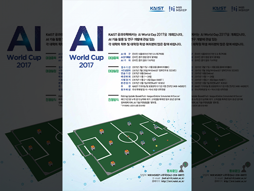 KAIST to Host the 2017 AI World Cup in November
KAIST, the birthplace of the Robot World Cup in 1996, now presents a new technology matchup, the AI World Cup this November, which will be held at KAIST. The event is being organized by the Machine Intelligence and Robotics Multi-Sponsored Research and Education Platform (MIR-MSREP) of KAIST. The online, simulated AI soccer game, based on rolling updates, will be a draw for avid online gamers and tech-savvy university students from around the nation.
The tournament is comprised of three events: ▲A 5 on 5 AI soccer match to be played after self-learning using AI technology in an online simulation environment ▲Commentary in which online soccer videos are analyzed and commented on, and ▲Game reporters who will write articles on online soccer event results.
The participants will undergo a month-long online practice period in October and compete in preliminary matches from November 1 through 24. The top teams that scored the highest accumulated points will compete in the finals on December 1. In the finals, each team’s AI technology implementation method will be evaluated to select the final winning team. To ensure a successful event, KAIST will host a briefing session for participants on July 28.
Technological prowess and early exposure to AI accumulated at KAIST led to the launching of this tournament. Professor Jong-Hwan Kim, the chair of the Organizing Committee of the AI World Cup, hosted the first ever Robot World Cup back in 1996. His concept has now evolved into the emerging technology of AI and the members of the Organizing Committee encompass the professors from the various departments of electrical engineering, computing, industrial and systems engineering, aerospace engineering, civil and environmental engineering, and the graduate schools of Green Transportation, Cultural Technology, and Science and Technology Policy.
In particular, ongoing convergence research initiatives incorporating AI into a wide arrays of disciplines such as bio, nano, and IT, played a crucial role for making this AI World Cup happen. Professor Kim said, “The winner of this year’s competition will be awarded a certificate and a small gift. In 2018, we aim to expand the event to an international scale by allowing international teams.”
Any undergraduate or graduate student in Korea can apply to participate in the ‘AI World Cup 2017’. KAIST will host a public trial event during the ‘Open KAIST’ event period to be held November 2-3 to help participating students understand the event better. ‘Open KAIST’ allows the general public to personally visit and experience what goes on in engineering departments and laboratories on the KAIST main campus. It is hosted by the College of Engineering every two years and is the largest event hosted by KAIST.
To participate in the ‘AI World Cup 2017,’ teams consisting of Korean undergraduates or graduate students can fill out application forms and submit them by September 30 on http://mir.kaist.ac.kr .
2017.07.14 View 13651
KAIST to Host the 2017 AI World Cup in November
KAIST, the birthplace of the Robot World Cup in 1996, now presents a new technology matchup, the AI World Cup this November, which will be held at KAIST. The event is being organized by the Machine Intelligence and Robotics Multi-Sponsored Research and Education Platform (MIR-MSREP) of KAIST. The online, simulated AI soccer game, based on rolling updates, will be a draw for avid online gamers and tech-savvy university students from around the nation.
The tournament is comprised of three events: ▲A 5 on 5 AI soccer match to be played after self-learning using AI technology in an online simulation environment ▲Commentary in which online soccer videos are analyzed and commented on, and ▲Game reporters who will write articles on online soccer event results.
The participants will undergo a month-long online practice period in October and compete in preliminary matches from November 1 through 24. The top teams that scored the highest accumulated points will compete in the finals on December 1. In the finals, each team’s AI technology implementation method will be evaluated to select the final winning team. To ensure a successful event, KAIST will host a briefing session for participants on July 28.
Technological prowess and early exposure to AI accumulated at KAIST led to the launching of this tournament. Professor Jong-Hwan Kim, the chair of the Organizing Committee of the AI World Cup, hosted the first ever Robot World Cup back in 1996. His concept has now evolved into the emerging technology of AI and the members of the Organizing Committee encompass the professors from the various departments of electrical engineering, computing, industrial and systems engineering, aerospace engineering, civil and environmental engineering, and the graduate schools of Green Transportation, Cultural Technology, and Science and Technology Policy.
In particular, ongoing convergence research initiatives incorporating AI into a wide arrays of disciplines such as bio, nano, and IT, played a crucial role for making this AI World Cup happen. Professor Kim said, “The winner of this year’s competition will be awarded a certificate and a small gift. In 2018, we aim to expand the event to an international scale by allowing international teams.”
Any undergraduate or graduate student in Korea can apply to participate in the ‘AI World Cup 2017’. KAIST will host a public trial event during the ‘Open KAIST’ event period to be held November 2-3 to help participating students understand the event better. ‘Open KAIST’ allows the general public to personally visit and experience what goes on in engineering departments and laboratories on the KAIST main campus. It is hosted by the College of Engineering every two years and is the largest event hosted by KAIST.
To participate in the ‘AI World Cup 2017,’ teams consisting of Korean undergraduates or graduate students can fill out application forms and submit them by September 30 on http://mir.kaist.ac.kr .
2017.07.14 View 13651 -
 Face Recognition System 'K-Eye' Presented by KAIST
Artificial intelligence (AI) is one of the key emerging technologies. Global IT companies are competitively launching the newest technologies and competition is heating up more than ever. However, most AI technologies focus on software and their operating speeds are low, making them a poor fit for mobile devices. Therefore, many big companies are investing to develop semiconductor chips for running AI programs with low power requirements but at high speeds.
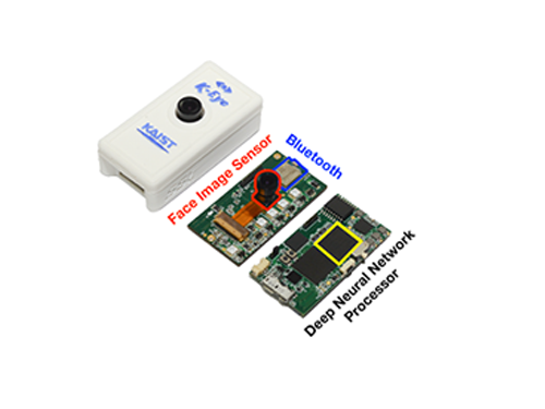
A research team led by Professor Hoi-Jun Yoo of the Department of Electrical Engineering has developed a semiconductor chip, CNNP (CNN Processor), that runs AI algorithms with ultra-low power, and K-Eye, a face recognition system using CNNP. The system was made in collaboration with a start-up company, UX Factory Co.
The K-Eye series consists of two types: a wearable type and a dongle type. The wearable type device can be used with a smartphone via Bluetooth, and it can operate for more than 24 hours with its internal battery. Users hanging K-Eye around their necks can conveniently check information about people by using their smartphone or smart watch, which connects K-Eye and allows users to access a database via their smart devices. A smartphone with K-EyeQ, the dongle type device, can recognize and share information about users at any time.
When recognizing that an authorized user is looking at its screen, the smartphone automatically turns on without a passcode, fingerprint, or iris authentication. Since it can distinguish whether an input face is coming from a saved photograph versus a real person, the smartphone cannot be tricked by the user’s photograph.
The K-Eye series carries other distinct features. It can detect a face at first and then recognize it, and it is possible to maintain “Always-on” status with low power consumption of less than 1mW. To accomplish this, the research team proposed two key technologies: an image sensor with “Always-on” face detection and the CNNP face recognition chip.
The first key technology, the “Always-on” image sensor, can determine if there is a face in its camera range. Then, it can capture frames and set the device to operate only when a face exists, reducing the standby power significantly. The face detection sensor combines analog and digital processing to reduce power consumption. With this approach, the analog processor, combined with the CMOS Image Sensor array, distinguishes the background area from the area likely to include a face, and the digital processor then detects the face only in the selected area. Hence, it becomes effective in terms of frame capture, face detection processing, and memory usage.
The second key technology, CNNP, achieved incredibly low power consumption by optimizing a convolutional neural network (CNN) in the areas of circuitry, architecture, and algorithms. First, the on-chip memory integrated in CNNP is specially designed to enable data to be read in a vertical direction as well as in a horizontal direction. Second, it has immense computational power with 1024 multipliers and accumulators operating in parallel and is capable of directly transferring the temporal results to each other without accessing to the external memory or on-chip communication network. Third, convolution calculations with a two-dimensional filter in the CNN algorithm are approximated into two sequential calculations of one-dimensional filters to achieve higher speeds and lower power consumption.
With these new technologies, CNNP achieved 97% high accuracy but consumed only 1/5000 power of the GPU. Face recognition can be performed with only 0.62mW of power consumption, and the chip can show higher performance than the GPU by using more power.
These chips were developed by Kyeongryeol Bong, a Ph. D. student under Professor Yoo and presented at the International Solid-State Circuit Conference (ISSCC) held in San Francisco in February. CNNP, which has the lowest reported power consumption in the world, has achieved a great deal of attention and has led to the development of the present K-Eye series for face recognition.
Professor Yoo said “AI - processors will lead the era of the Fourth Industrial Revolution. With the development of this AI chip, we expect Korea to take the lead in global AI technology.”
The research team and UX Factory Co. are preparing to commercialize the K-Eye series by the end of this year. According to a market researcher IDC, the market scale of the AI industry will grow from $127 billion last year to $165 billion in this year.
(Photo caption: Schematic diagram of K-Eye system)
2017.06.14 View 17839
Face Recognition System 'K-Eye' Presented by KAIST
Artificial intelligence (AI) is one of the key emerging technologies. Global IT companies are competitively launching the newest technologies and competition is heating up more than ever. However, most AI technologies focus on software and their operating speeds are low, making them a poor fit for mobile devices. Therefore, many big companies are investing to develop semiconductor chips for running AI programs with low power requirements but at high speeds.
A research team led by Professor Hoi-Jun Yoo of the Department of Electrical Engineering has developed a semiconductor chip, CNNP (CNN Processor), that runs AI algorithms with ultra-low power, and K-Eye, a face recognition system using CNNP. The system was made in collaboration with a start-up company, UX Factory Co.
The K-Eye series consists of two types: a wearable type and a dongle type. The wearable type device can be used with a smartphone via Bluetooth, and it can operate for more than 24 hours with its internal battery. Users hanging K-Eye around their necks can conveniently check information about people by using their smartphone or smart watch, which connects K-Eye and allows users to access a database via their smart devices. A smartphone with K-EyeQ, the dongle type device, can recognize and share information about users at any time.
When recognizing that an authorized user is looking at its screen, the smartphone automatically turns on without a passcode, fingerprint, or iris authentication. Since it can distinguish whether an input face is coming from a saved photograph versus a real person, the smartphone cannot be tricked by the user’s photograph.
The K-Eye series carries other distinct features. It can detect a face at first and then recognize it, and it is possible to maintain “Always-on” status with low power consumption of less than 1mW. To accomplish this, the research team proposed two key technologies: an image sensor with “Always-on” face detection and the CNNP face recognition chip.
The first key technology, the “Always-on” image sensor, can determine if there is a face in its camera range. Then, it can capture frames and set the device to operate only when a face exists, reducing the standby power significantly. The face detection sensor combines analog and digital processing to reduce power consumption. With this approach, the analog processor, combined with the CMOS Image Sensor array, distinguishes the background area from the area likely to include a face, and the digital processor then detects the face only in the selected area. Hence, it becomes effective in terms of frame capture, face detection processing, and memory usage.
The second key technology, CNNP, achieved incredibly low power consumption by optimizing a convolutional neural network (CNN) in the areas of circuitry, architecture, and algorithms. First, the on-chip memory integrated in CNNP is specially designed to enable data to be read in a vertical direction as well as in a horizontal direction. Second, it has immense computational power with 1024 multipliers and accumulators operating in parallel and is capable of directly transferring the temporal results to each other without accessing to the external memory or on-chip communication network. Third, convolution calculations with a two-dimensional filter in the CNN algorithm are approximated into two sequential calculations of one-dimensional filters to achieve higher speeds and lower power consumption.
With these new technologies, CNNP achieved 97% high accuracy but consumed only 1/5000 power of the GPU. Face recognition can be performed with only 0.62mW of power consumption, and the chip can show higher performance than the GPU by using more power.
These chips were developed by Kyeongryeol Bong, a Ph. D. student under Professor Yoo and presented at the International Solid-State Circuit Conference (ISSCC) held in San Francisco in February. CNNP, which has the lowest reported power consumption in the world, has achieved a great deal of attention and has led to the development of the present K-Eye series for face recognition.
Professor Yoo said “AI - processors will lead the era of the Fourth Industrial Revolution. With the development of this AI chip, we expect Korea to take the lead in global AI technology.”
The research team and UX Factory Co. are preparing to commercialize the K-Eye series by the end of this year. According to a market researcher IDC, the market scale of the AI industry will grow from $127 billion last year to $165 billion in this year.
(Photo caption: Schematic diagram of K-Eye system)
2017.06.14 View 17839 -
 A Transport Technology for Nanowires Thermally Treated at 700 Celsius Degrees
Professor Jun-Bo Yoon and his research team of the Department of Electrical Engineering at KAIST developed a technology for transporting thermally treated nanowires to a flexible substrate and created a high performance device for collecting flexible energy by using the new technology.
Mr. Min-Ho Seo, a Ph.D. candidate, participated in this study as the first author. The results were published online on January 30th in ACS Nano, an international journal in the field of nanoscience and engineering. (“Versatile Transfer of an Ultralong and Seamless Nanowire Array Crystallized at High Temperature for Use in High-performance Flexible Devices,” DOI: 10.1021/acsnano.6b06842)
Nanowires are one of the most representative nanomaterials. They have wire structures with dimensions in nanometers. The nanowires are widely used in the scientific and engineering fields due to their prominent physical and chemical properties that depend on a one-dimensional structure, and their high applicability.
Nanowires have much higher performance if their structure has unique features such as an excellent arrangement and a longer-than-average length. Many researchers are thus actively participating in the research for making nanowires without much difficulty, analyzing them, and developing them for high performance application devices.
Scientists have recently favored a research topic on making nanowires chemically and physically on a flexible substrate and applies the nanowires to a flexible electric device such as a high performance wearable sensor.
The existing technology, however, mixed nanowires from a chemical synthesis with a solution and spread the mixture on a flexible substrate. The resultant distribution was random, and it was difficult to produce a high performance device based on the structural advantages of nanowires. In addition, the technology used a cutting edge nano-process and flexible materials, but this was not economically beneficial. The production of stable materials at a temperature of 700 Celsius degrees or higher is unattainable, a great challenge for the application.
To solve this problem, the research team developed a new nano-transfer technology that combines a silicon nano-grating board with a large surface area and a nano-sacrificial layer process. A nano-sacrificial layer exists between nanowires and a nano-grating board, which acts as the mold for the nano-transfer. The new technology allows the device undergo thermal treatment. After this, the layer disappears when the nanowires are transported to a flexible substrate.
This technology also permits the stable production of nanowires with secured properties at an extremely high temperature. In this case, the nanowires are neatly organized on a flexible substrate. The research team used the technology to manufacture barium carbonate nanowires on top of the flexible substrate. The wires secured their properties at a temperature of 700℃ or above. The team employed the collection of wearable energy to obtain much higher electrical energy than that of an energy collecting device designed based on regular barium titanate nanowires.
The researchers said that their technology is built upon a semiconductor process, known as Physical Vapor Deposition that allows various materials such as ceramics and semiconductors to be used for flexible substrates of nanowires. They expected that high performance flexible electric devices such as flexible transistors and thermoelectric elements can be produced with this method.
Mr. Seo said, “In this study, we transported nanowire materials with developed properties on a flexible substrate and showed an increase in device performance. Our technology will be fundamental to the production of various nanowires on a flexible substrate as well as the feasibility of making high performance wearable electric devices.”
This research was supported by the Leap Research Support Program of the National Research Foundation of Korea.
Fig. 1. Transcription process of new, developed nanowires (a) and a fundamental mimetic diagram of a nano-sacrificial layer (b)
Fig. 2. Transcription results from using gold (AU) nanowires. The categories of the results were (a) optical images, (b) physical signals, (c) cross-sectional images from a scanning electron microscope (SEM), and (d-f) an electric verification of whether the perfectly arranged nanowires were made on a large surface.
Fig. 3. Transcription from using barium titanate (BaTiO3) nanowires. The results were (a) optical images, (b-e) top images taken from an SEM in various locations, and (f, g) property analysis.
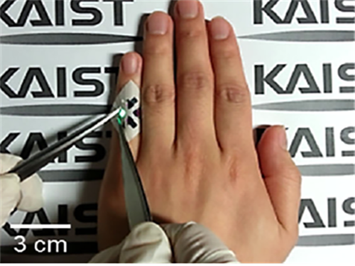
Fig. 4. Mimetic diagram of the energy collecting device from using a BaTiO3 nanowire substrate and an optical image of the experiment for the miniature energy collecting device attached to an index finger.
2017.03.22 View 10556
A Transport Technology for Nanowires Thermally Treated at 700 Celsius Degrees
Professor Jun-Bo Yoon and his research team of the Department of Electrical Engineering at KAIST developed a technology for transporting thermally treated nanowires to a flexible substrate and created a high performance device for collecting flexible energy by using the new technology.
Mr. Min-Ho Seo, a Ph.D. candidate, participated in this study as the first author. The results were published online on January 30th in ACS Nano, an international journal in the field of nanoscience and engineering. (“Versatile Transfer of an Ultralong and Seamless Nanowire Array Crystallized at High Temperature for Use in High-performance Flexible Devices,” DOI: 10.1021/acsnano.6b06842)
Nanowires are one of the most representative nanomaterials. They have wire structures with dimensions in nanometers. The nanowires are widely used in the scientific and engineering fields due to their prominent physical and chemical properties that depend on a one-dimensional structure, and their high applicability.
Nanowires have much higher performance if their structure has unique features such as an excellent arrangement and a longer-than-average length. Many researchers are thus actively participating in the research for making nanowires without much difficulty, analyzing them, and developing them for high performance application devices.
Scientists have recently favored a research topic on making nanowires chemically and physically on a flexible substrate and applies the nanowires to a flexible electric device such as a high performance wearable sensor.
The existing technology, however, mixed nanowires from a chemical synthesis with a solution and spread the mixture on a flexible substrate. The resultant distribution was random, and it was difficult to produce a high performance device based on the structural advantages of nanowires. In addition, the technology used a cutting edge nano-process and flexible materials, but this was not economically beneficial. The production of stable materials at a temperature of 700 Celsius degrees or higher is unattainable, a great challenge for the application.
To solve this problem, the research team developed a new nano-transfer technology that combines a silicon nano-grating board with a large surface area and a nano-sacrificial layer process. A nano-sacrificial layer exists between nanowires and a nano-grating board, which acts as the mold for the nano-transfer. The new technology allows the device undergo thermal treatment. After this, the layer disappears when the nanowires are transported to a flexible substrate.
This technology also permits the stable production of nanowires with secured properties at an extremely high temperature. In this case, the nanowires are neatly organized on a flexible substrate. The research team used the technology to manufacture barium carbonate nanowires on top of the flexible substrate. The wires secured their properties at a temperature of 700℃ or above. The team employed the collection of wearable energy to obtain much higher electrical energy than that of an energy collecting device designed based on regular barium titanate nanowires.
The researchers said that their technology is built upon a semiconductor process, known as Physical Vapor Deposition that allows various materials such as ceramics and semiconductors to be used for flexible substrates of nanowires. They expected that high performance flexible electric devices such as flexible transistors and thermoelectric elements can be produced with this method.
Mr. Seo said, “In this study, we transported nanowire materials with developed properties on a flexible substrate and showed an increase in device performance. Our technology will be fundamental to the production of various nanowires on a flexible substrate as well as the feasibility of making high performance wearable electric devices.”
This research was supported by the Leap Research Support Program of the National Research Foundation of Korea.
Fig. 1. Transcription process of new, developed nanowires (a) and a fundamental mimetic diagram of a nano-sacrificial layer (b)
Fig. 2. Transcription results from using gold (AU) nanowires. The categories of the results were (a) optical images, (b) physical signals, (c) cross-sectional images from a scanning electron microscope (SEM), and (d-f) an electric verification of whether the perfectly arranged nanowires were made on a large surface.
Fig. 3. Transcription from using barium titanate (BaTiO3) nanowires. The results were (a) optical images, (b-e) top images taken from an SEM in various locations, and (f, g) property analysis.
Fig. 4. Mimetic diagram of the energy collecting device from using a BaTiO3 nanowire substrate and an optical image of the experiment for the miniature energy collecting device attached to an index finger.
2017.03.22 View 10556 -
 An Improved Carbon Nanotube Semiconductor
Professor Yang-Kyu Choi and his research team of the School of Electrical Engineering at KAIST collaborated with Professor Sung-Jin Choi of Kookmin University to develop a large-scale carbon nanotube semiconductor by using a 3-D fin-gate structure with carbon nanotubes on its top.
Dong Il Lee, a postdoctoral researcher at KAIST’s Electrical Engineering School, participated in this study as the first author. It was published in ACS Nano on November 10, 2016, and was entitled “Three-Dimensional Fin-Structured Semiconducting Carbon Nanotube Network Transistor.”
A semiconductor made with carbon nanotubes operates faster than a silicon semiconductor and requires less energy, yielding higher performance.
Most electronic equipment and devices, however, use silicon semiconductors because it is difficult to fabricate highly purified and densely packed semiconductors with carbon nanotubes (CNTs).
To date, the performance of CNTs was limited due to their low density. Their purity was also low, so it was impossible to make products that had a constant yield on a large-surface wafer or substrate. These characteristics made the mass production of semiconducting CNTs difficult.
To solve these difficulties, the research team used a 3-D fin-gate to vapor-deposit carbon nanotubes on its top. They developed a semiconductor that had a high current density with a width less than 50 nm.
The three-dimensional fin structure was able to vapor-deposit 600 carbon nanotubes per micrometer. This structure could have 20 times more nanotubes than the two dimensional structure, which could only vapor-deposit thirty in the same 1 micrometer width.
In addition, the research team used semi-conductive carbon nanotubes having a purity rating higher than 99.9% from a previous study to obtain a high yield semiconductor.
The semiconductor from the research group has a high current density even with a width less than 50 μm. The new semiconductor is expected to be five times faster than a silicon-based semiconductor and will require five times less electricity during operation.
Furthermore, the new semiconductor can be made by or will be compatible with the equipment for producing silicon-based semiconductors, so there will be no additional costs.
Researcher Lee said, “As a next generation semiconductor, the carbon nanotube semiconductor will have better performance, and its effectiveness will be higher.” He also added, “Hopefully, the new semiconductor will replace the silicon-based semiconductors in ten years.”
This study received support from the Center for Integrated Smart Sensors funded by the Ministry of Science, ICT & Future Planning of Korea as the Global Frontier Project, and from the CMOS (Complementary Metal-Oxide-Semiconductor) THz Technology Convergence Center of the Pioneer Research Center Program sponsored by the National Research Foundation of Korea.
Picture 1: 3D Diagram of the Carbon Nanotube Electronic Device and Its Scanning Electron Microscope (SEM) Image
Picture 2: 3D Transistor Device on an 8-inch Base and the SEM Image of Its Cross Section
2017.02.16 View 12701
An Improved Carbon Nanotube Semiconductor
Professor Yang-Kyu Choi and his research team of the School of Electrical Engineering at KAIST collaborated with Professor Sung-Jin Choi of Kookmin University to develop a large-scale carbon nanotube semiconductor by using a 3-D fin-gate structure with carbon nanotubes on its top.
Dong Il Lee, a postdoctoral researcher at KAIST’s Electrical Engineering School, participated in this study as the first author. It was published in ACS Nano on November 10, 2016, and was entitled “Three-Dimensional Fin-Structured Semiconducting Carbon Nanotube Network Transistor.”
A semiconductor made with carbon nanotubes operates faster than a silicon semiconductor and requires less energy, yielding higher performance.
Most electronic equipment and devices, however, use silicon semiconductors because it is difficult to fabricate highly purified and densely packed semiconductors with carbon nanotubes (CNTs).
To date, the performance of CNTs was limited due to their low density. Their purity was also low, so it was impossible to make products that had a constant yield on a large-surface wafer or substrate. These characteristics made the mass production of semiconducting CNTs difficult.
To solve these difficulties, the research team used a 3-D fin-gate to vapor-deposit carbon nanotubes on its top. They developed a semiconductor that had a high current density with a width less than 50 nm.
The three-dimensional fin structure was able to vapor-deposit 600 carbon nanotubes per micrometer. This structure could have 20 times more nanotubes than the two dimensional structure, which could only vapor-deposit thirty in the same 1 micrometer width.
In addition, the research team used semi-conductive carbon nanotubes having a purity rating higher than 99.9% from a previous study to obtain a high yield semiconductor.
The semiconductor from the research group has a high current density even with a width less than 50 μm. The new semiconductor is expected to be five times faster than a silicon-based semiconductor and will require five times less electricity during operation.
Furthermore, the new semiconductor can be made by or will be compatible with the equipment for producing silicon-based semiconductors, so there will be no additional costs.
Researcher Lee said, “As a next generation semiconductor, the carbon nanotube semiconductor will have better performance, and its effectiveness will be higher.” He also added, “Hopefully, the new semiconductor will replace the silicon-based semiconductors in ten years.”
This study received support from the Center for Integrated Smart Sensors funded by the Ministry of Science, ICT & Future Planning of Korea as the Global Frontier Project, and from the CMOS (Complementary Metal-Oxide-Semiconductor) THz Technology Convergence Center of the Pioneer Research Center Program sponsored by the National Research Foundation of Korea.
Picture 1: 3D Diagram of the Carbon Nanotube Electronic Device and Its Scanning Electron Microscope (SEM) Image
Picture 2: 3D Transistor Device on an 8-inch Base and the SEM Image of Its Cross Section
2017.02.16 View 12701 -
 Extremely Thin and Highly Flexible Graphene-Based Thermoacoustic Speakers
A joint research team led by Professors Jung-Woo Choi and Byung Jin Cho of the School of Electrical Engineering and Professor Sang Ouk Kim of the Material Science and Engineering Department, all on the faculty of the Korea Advanced Institute of Science and Technology (KAIST), has developed a simpler way to mass-produce ultra-thin graphene thermosacoustic speakers.
Their research results were published online on August 17, 2016 in a journal called Applied Materials & Interfaces. The IEEE Spectrum, a monthly magazine published by the Institute of Electrical and Electronics Engineers, reported on the research on September 9, 2016, in an article titled, “Graphene Enables Flat Speakers for Mobile Audio Systems.” The American Chemical Society also drew attention to the team’s work in its article dated September 7, 2016, “Bringing Graphene Speakers to the Mobile Market.”
Thermoacoustic speakers generate sound waves from temperature fluctuations by rapidly heating and cooling conducting materials. Unlike conventional voice-coil speakers, thermoacoustic speakers do not rely on vibrations to produce sound, and thus do not need bulky acoustic boxes to keep complicated mechanical parts for sound production. They also generate good quality sound in all directions, enabling them to be placed on any surface including curved ones without canceling out sounds generated from opposite sides.
Based on a two-step, template-free fabrication method that involved freeze-drying a solution of graphene oxide flakes and the reduction/doping of oxidized graphene to improve electrical properties, the research team produced a N-doped, three-dimensional (3D), reduced graphene oxide aerogel (N-rGOA) with a porous macroscopic structure that permitted easy modulation for many potential applications.
Using 3D graphene aerogels, the team succeeded in fabricating an array of loudspeakers that were able to withstand over 40 W input power and that showed excellent sound pressure level (SPL), comparable to those of previously reported 2D and 3D graphene loudspeakers.
Choong Sun Kim, the lead author of the research paper and a doctoral student in the School of Electrical Engineering at KAIST, said:
“Thermoacoustic speakers have a higher efficiency when conducting materials have a smaller heat capacity. Nanomaterials such as graphene are an ideal candidate for conductors, but they require a substrate to support their extremely thinness. The substrate’s tendency to lose heat lowers the speakers’ efficiency. Here, we developed 3D graphene aerogels without a substrate by using a simple two-step process. With graphene aerogels, we have fabricated an array of loudspeakers that demonstrated stable performance. This is a practical technology that will enable mass-production of thermosacoustic speakers including on mobile platforms.”
The research paper is entitled “Application of N-Doped Three-Dimensional Reduced Graphene Oxide Aerogel to Thin Film Loudspeaker.” (DOI: 10.1021/acsami.6b03618)
Figure 1: A Thermoacoustic Loudspeaker Consisted of an Array of 16 3D Graphene Aerogels
Figure 2: Two-step Fabrication Process of 3D Reduced Graphene Oxide Aerogel Using Freeze-Drying and Reduction/Doping
Figure 3: X-ray Photoelectron Spectroscopy Graph of the 3D Reduced Graphene Oxide Aerogel and Its Scanning Electron Microscope Image
2016.10.05 View 15878
Extremely Thin and Highly Flexible Graphene-Based Thermoacoustic Speakers
A joint research team led by Professors Jung-Woo Choi and Byung Jin Cho of the School of Electrical Engineering and Professor Sang Ouk Kim of the Material Science and Engineering Department, all on the faculty of the Korea Advanced Institute of Science and Technology (KAIST), has developed a simpler way to mass-produce ultra-thin graphene thermosacoustic speakers.
Their research results were published online on August 17, 2016 in a journal called Applied Materials & Interfaces. The IEEE Spectrum, a monthly magazine published by the Institute of Electrical and Electronics Engineers, reported on the research on September 9, 2016, in an article titled, “Graphene Enables Flat Speakers for Mobile Audio Systems.” The American Chemical Society also drew attention to the team’s work in its article dated September 7, 2016, “Bringing Graphene Speakers to the Mobile Market.”
Thermoacoustic speakers generate sound waves from temperature fluctuations by rapidly heating and cooling conducting materials. Unlike conventional voice-coil speakers, thermoacoustic speakers do not rely on vibrations to produce sound, and thus do not need bulky acoustic boxes to keep complicated mechanical parts for sound production. They also generate good quality sound in all directions, enabling them to be placed on any surface including curved ones without canceling out sounds generated from opposite sides.
Based on a two-step, template-free fabrication method that involved freeze-drying a solution of graphene oxide flakes and the reduction/doping of oxidized graphene to improve electrical properties, the research team produced a N-doped, three-dimensional (3D), reduced graphene oxide aerogel (N-rGOA) with a porous macroscopic structure that permitted easy modulation for many potential applications.
Using 3D graphene aerogels, the team succeeded in fabricating an array of loudspeakers that were able to withstand over 40 W input power and that showed excellent sound pressure level (SPL), comparable to those of previously reported 2D and 3D graphene loudspeakers.
Choong Sun Kim, the lead author of the research paper and a doctoral student in the School of Electrical Engineering at KAIST, said:
“Thermoacoustic speakers have a higher efficiency when conducting materials have a smaller heat capacity. Nanomaterials such as graphene are an ideal candidate for conductors, but they require a substrate to support their extremely thinness. The substrate’s tendency to lose heat lowers the speakers’ efficiency. Here, we developed 3D graphene aerogels without a substrate by using a simple two-step process. With graphene aerogels, we have fabricated an array of loudspeakers that demonstrated stable performance. This is a practical technology that will enable mass-production of thermosacoustic speakers including on mobile platforms.”
The research paper is entitled “Application of N-Doped Three-Dimensional Reduced Graphene Oxide Aerogel to Thin Film Loudspeaker.” (DOI: 10.1021/acsami.6b03618)
Figure 1: A Thermoacoustic Loudspeaker Consisted of an Array of 16 3D Graphene Aerogels
Figure 2: Two-step Fabrication Process of 3D Reduced Graphene Oxide Aerogel Using Freeze-Drying and Reduction/Doping
Figure 3: X-ray Photoelectron Spectroscopy Graph of the 3D Reduced Graphene Oxide Aerogel and Its Scanning Electron Microscope Image
2016.10.05 View 15878 -
 KAIST Team Develops Semi-Transparent Solar Cells with Thermal Mirror Capability
A research team led by KAIST and Sungkyunkwan University professors has created semi-transparent perovskite solar cells that demonstrate high-power conversion efficiency and transmit visible light while blocking infrared light, making them great candidates for solar windows.
Modern architects prefer to build exteriors designed with glass mainly from artistic or cost perspectives. Scientists, however, go one step further and see opportunities from its potential ability to harness solar energy. Researchers have thus explored ways to make solar cells transparent or semi-transparent as a substitute material for glass, but this has proven to be a challenging task because solar cells need to absorb sunlight to generate electricity, and when they are transparent, it reduces their energy efficiency.
Typical solar cells today are made of crystalline silicon, but it is difficult to make them translucent. Semi-transparent solar cells under development use, for example, organic or dye-sensitized materials, but compared to crystalline silicon-based cells, their power-conversion efficiencies are relatively low. Perovskites are hybrid organic-inorganic halide-based photovoltaic materials, which are cheap to produce and easy to manufacture. They have recently received much attention as the efficiency of perovskite solar cells has rapidly increased to the level of silicon technologies in the past few years.
Using perovskites, a Korean research team led by Professor Seunghyup Yoo of the Electrical Engineering School at KAIST and Professor Nam-Gyu Park of the Chemical Engineering School at Sungkyunkwan University developed a semi-transparent solar cell that is highly efficient and, additionally, functions very effectively as a thermal-mirror.
The team has developed a top transparent electrode (TTE) that works well with perovskite solar cells. In most cases, a key to success in realizing semi-transparent solar cells is to find a TTE that is compatible with a given photoactive material system, which is also the case for perovskite solar cells. The proposed TTE is based on a multilayer stack consisting of a metal film sandwiched between a high refractive-index (high-index) layer and an interfacial buffer layer. This TTE, placed as a top-most layer, can be prepared without damaging ingredients used in perovskite solar cells. Unlike conventional transparent electrodes focusing only on transmitting visible light, the proposed TTE plays the dual role of passing through visible light while reflecting infrared rays. The semi-transparent solar cells made with the proposed TTEs exhibited average power conversion efficiency as high as 13.3% with 85.5% infrared rejection.
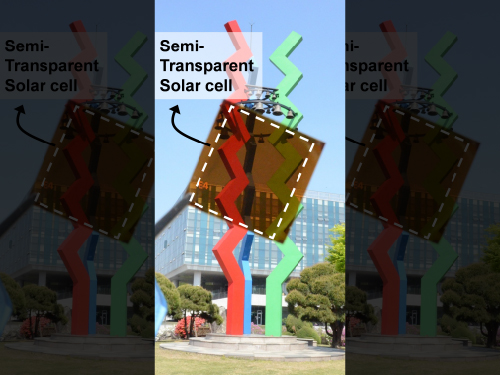
The team believes that if the semi-transparent perovskite solar cells are scaled up for practical applications, they can be used in solar windows for buildings and automobiles, which not only generate electrical energy but also enable the smart heat management for indoor environments, thereby utilizing solar energy more efficiently and effectively.
This result was published as a cover article in the July 20, 2016 issue of Advanced Energy Materials. The research paper is entitled “Empowering Semi-transparent Solar Cells with Thermal-mirror Functionality.” (DOI: 10.1002/aenm.201502466)
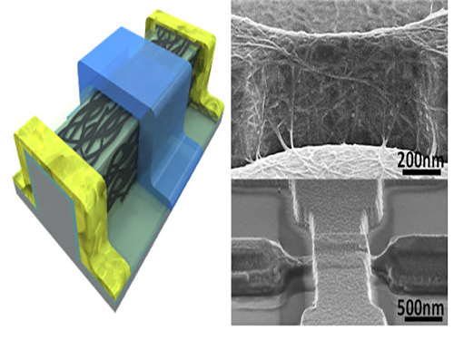
The team designed the transparent electrode (TE) stack in three layers: A thin-film of silver (Ag) is placed in between the bottom interfacial layer of molybdenum trioxide (MoO3) and the top high-index dielectric layer of zinc sulfide (ZnS). Such a tri-layer approach has been known as a means to increase the overall visible-light transmittance of metallic thin films via index matching technique, which is essentially the same technique used for anti-reflection coating of glasses except that the present case involves a metallic layer.
Traditionally, when a TE is based on a metal film, such as Ag, the film should be extremely thin, e.g., 7-12 nanometers (nm), to obtain transparency and, accordingly, to transmit visible light. However, the team took a different approach in this research. They made the Ag TE two or three times thicker (12-24 nm) than conventional metal films and, as a result, it reflected more infrared light. The high refractive index of the ZnS layer plays an essential role in keeping the visible light transmittance of the proposed TTE high even with the relatively thick Ag film when its thickness is carefully optimized for maximal destructive interference, leading to low reflectance (and thus high transmittance) within its visible light range.
The team confirmed the semi-transparent perovskite solar cell’s thermal-mirror function through an experiment in which a halogen lamp illuminated an object for five minutes through three mediums: a window of bare glass, automotive tinting film, and the proposed semi-transparent perovskite solar cell. An infrared (IR) camera took thermal images of the object as well as that of each window’s surface. The object’s temperature, when exposed through the glass window, rose to 36.8 Celsius degrees whereas both the tinting film and the cell allowed the object to remain below 27 Celsius degrees. The tinting film absorbs light to block solar energy, so the film’s surface became hot as it was continuously exposed to the lamp light, but the proposed semi-transparent solar cell stayed cool since it rejects solar heat energy by reflection, rather than by absorption. The total solar energy rejection (TSER) of the proposed cell was as high as 89.6%.
Professor Yoo of KAIST said, “The major contributions of this work are to find transparent electrode technology suitable for translucent perovskite cells and to provide a design approach to fully harness the potential it can further deliver as a heat mirror in addition to its main role as an electrode. The present work can be further fine-tuned to include colored solar cells and to incorporate flexible or rollable form factors, as they will allow for greater design freedom and thus offer more opportunities for them to be integrated into real-world objects and structures such as cars, buildings, and houses.”
The lead authors are Hoyeon Kim and Jaewon Ha, both Ph.D. candidates in the School of Electrical Engineering at KAIST, and Hui-Seon Kim, a student in the School of Chemical Engineering at Sungkyunkwan University. This research was supported mainly by the Climate Change Research Hub Program of KAIST.
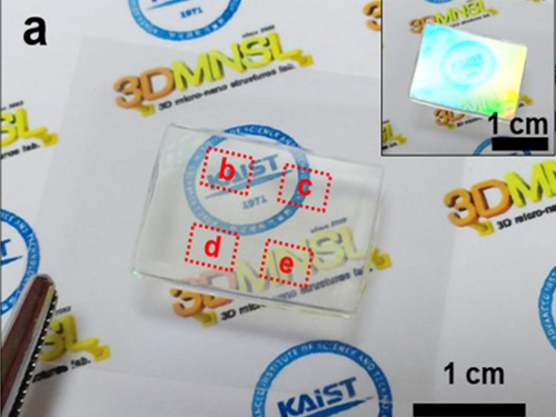
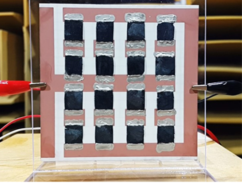
Picture 1: Semi-transparent Perovskite Solar Cell
This picture shows a prototype of a semi-transparent perovskite solar cell with thermal-mirror functionality.
Picture 2: A Heat Rejection Performance Comparison Experiment
This picture presents thermal images taken by an infrared camera for comparing the heat rejection performance of bare glass, automotive tinting film, and a semi-transparent perovskite solar cell after being illuminated by a halogen lamp for five minutes.
2016.08.02 View 13780
KAIST Team Develops Semi-Transparent Solar Cells with Thermal Mirror Capability
A research team led by KAIST and Sungkyunkwan University professors has created semi-transparent perovskite solar cells that demonstrate high-power conversion efficiency and transmit visible light while blocking infrared light, making them great candidates for solar windows.
Modern architects prefer to build exteriors designed with glass mainly from artistic or cost perspectives. Scientists, however, go one step further and see opportunities from its potential ability to harness solar energy. Researchers have thus explored ways to make solar cells transparent or semi-transparent as a substitute material for glass, but this has proven to be a challenging task because solar cells need to absorb sunlight to generate electricity, and when they are transparent, it reduces their energy efficiency.
Typical solar cells today are made of crystalline silicon, but it is difficult to make them translucent. Semi-transparent solar cells under development use, for example, organic or dye-sensitized materials, but compared to crystalline silicon-based cells, their power-conversion efficiencies are relatively low. Perovskites are hybrid organic-inorganic halide-based photovoltaic materials, which are cheap to produce and easy to manufacture. They have recently received much attention as the efficiency of perovskite solar cells has rapidly increased to the level of silicon technologies in the past few years.
Using perovskites, a Korean research team led by Professor Seunghyup Yoo of the Electrical Engineering School at KAIST and Professor Nam-Gyu Park of the Chemical Engineering School at Sungkyunkwan University developed a semi-transparent solar cell that is highly efficient and, additionally, functions very effectively as a thermal-mirror.
The team has developed a top transparent electrode (TTE) that works well with perovskite solar cells. In most cases, a key to success in realizing semi-transparent solar cells is to find a TTE that is compatible with a given photoactive material system, which is also the case for perovskite solar cells. The proposed TTE is based on a multilayer stack consisting of a metal film sandwiched between a high refractive-index (high-index) layer and an interfacial buffer layer. This TTE, placed as a top-most layer, can be prepared without damaging ingredients used in perovskite solar cells. Unlike conventional transparent electrodes focusing only on transmitting visible light, the proposed TTE plays the dual role of passing through visible light while reflecting infrared rays. The semi-transparent solar cells made with the proposed TTEs exhibited average power conversion efficiency as high as 13.3% with 85.5% infrared rejection.
The team believes that if the semi-transparent perovskite solar cells are scaled up for practical applications, they can be used in solar windows for buildings and automobiles, which not only generate electrical energy but also enable the smart heat management for indoor environments, thereby utilizing solar energy more efficiently and effectively.
This result was published as a cover article in the July 20, 2016 issue of Advanced Energy Materials. The research paper is entitled “Empowering Semi-transparent Solar Cells with Thermal-mirror Functionality.” (DOI: 10.1002/aenm.201502466)
The team designed the transparent electrode (TE) stack in three layers: A thin-film of silver (Ag) is placed in between the bottom interfacial layer of molybdenum trioxide (MoO3) and the top high-index dielectric layer of zinc sulfide (ZnS). Such a tri-layer approach has been known as a means to increase the overall visible-light transmittance of metallic thin films via index matching technique, which is essentially the same technique used for anti-reflection coating of glasses except that the present case involves a metallic layer.
Traditionally, when a TE is based on a metal film, such as Ag, the film should be extremely thin, e.g., 7-12 nanometers (nm), to obtain transparency and, accordingly, to transmit visible light. However, the team took a different approach in this research. They made the Ag TE two or three times thicker (12-24 nm) than conventional metal films and, as a result, it reflected more infrared light. The high refractive index of the ZnS layer plays an essential role in keeping the visible light transmittance of the proposed TTE high even with the relatively thick Ag film when its thickness is carefully optimized for maximal destructive interference, leading to low reflectance (and thus high transmittance) within its visible light range.
The team confirmed the semi-transparent perovskite solar cell’s thermal-mirror function through an experiment in which a halogen lamp illuminated an object for five minutes through three mediums: a window of bare glass, automotive tinting film, and the proposed semi-transparent perovskite solar cell. An infrared (IR) camera took thermal images of the object as well as that of each window’s surface. The object’s temperature, when exposed through the glass window, rose to 36.8 Celsius degrees whereas both the tinting film and the cell allowed the object to remain below 27 Celsius degrees. The tinting film absorbs light to block solar energy, so the film’s surface became hot as it was continuously exposed to the lamp light, but the proposed semi-transparent solar cell stayed cool since it rejects solar heat energy by reflection, rather than by absorption. The total solar energy rejection (TSER) of the proposed cell was as high as 89.6%.
Professor Yoo of KAIST said, “The major contributions of this work are to find transparent electrode technology suitable for translucent perovskite cells and to provide a design approach to fully harness the potential it can further deliver as a heat mirror in addition to its main role as an electrode. The present work can be further fine-tuned to include colored solar cells and to incorporate flexible or rollable form factors, as they will allow for greater design freedom and thus offer more opportunities for them to be integrated into real-world objects and structures such as cars, buildings, and houses.”
The lead authors are Hoyeon Kim and Jaewon Ha, both Ph.D. candidates in the School of Electrical Engineering at KAIST, and Hui-Seon Kim, a student in the School of Chemical Engineering at Sungkyunkwan University. This research was supported mainly by the Climate Change Research Hub Program of KAIST.
Picture 1: Semi-transparent Perovskite Solar Cell
This picture shows a prototype of a semi-transparent perovskite solar cell with thermal-mirror functionality.
Picture 2: A Heat Rejection Performance Comparison Experiment
This picture presents thermal images taken by an infrared camera for comparing the heat rejection performance of bare glass, automotive tinting film, and a semi-transparent perovskite solar cell after being illuminated by a halogen lamp for five minutes.
2016.08.02 View 13780 -
 Graphene-Based Transparent Electrodes for Highly Efficient Flexible OLEDs
A Korean research team developed an ideal electrode structure composed of graphene and layers of titanium dioxide and conducting polymers, resulting in highly flexible and efficient OLEDs.
The arrival of a thin and lightweight computer that even rolls up like a piece of paper will not be in the far distant future. Flexible organic light-emitting diodes (OLEDs), built upon a plastic substrate, have received greater attention lately for their use in next-generation displays that can be bent or rolled while still operating.
A Korean research team led by Professor Seunghyup Yoo from the School of Electrical Engineering, KAIST and Professor Tae-Woo Lee from the Department of Materials Science and Engineering, Pohang University of Science and Technology (POSTECH) has developed highly flexible OLEDs with excellent efficiency by using graphene as a transparent electrode (TE) which is placed in between titanium dioxide (TiO2) and conducting polymer layers. The research results were published online on June 2, 2016 in Nature Communications.
OLEDs are stacked in several ultra-thin layers on glass, foil, or plastic substrates, in which multi-layers of organic compounds are sandwiched between two electrodes (cathode and anode). When voltage is applied across the electrodes, electrons from the cathode and holes (positive charges) from the anode draw toward each other and meet in the emissive layer. OLEDs emit light as an electron recombines with a positive hole, releasing energy in the form of a photon. One of the electrodes in OLEDs is usually transparent, and depending on which electrode is transparent, OLEDs can either emit from the top or bottom.
In conventional bottom-emission OLEDs, an anode is transparent in order for the emitted photons to exit the device through its substrate. Indium-tin-oxide (ITO) is commonly used as a transparent anode because of its high transparency, low sheet resistance, and well-established manufacturing process. However, ITO can potentially be expensive, and moreover, is brittle, being susceptible to bending-induced formation of cracks.
Graphene, a two-dimensional thin layer of carbon atoms tightly bonded together in a hexagonal honeycomb lattice, has recently emerged as an alternative to ITO. With outstanding electrical, physical, and chemical properties, its atomic thinness leading to a high degree of flexibility and transparency makes it an ideal candidate for TEs. Nonetheless, the efficiency of graphene-based OLEDs reported to date has been, at best, about the same level of ITO-based OLEDs.
As a solution, the Korean research team, which further includes Professors Sung-Yool Choi (Electrical Engineering) and Taek-Soo Kim (Mechanical Engineering) of KAIST and their students, proposed a new device architecture that can maximize the efficiency of graphene-based OLEDs. They fabricated a transparent anode in a composite structure in which a TiO2 layer with a high refractive index (high-n) and a hole-injection layer (HIL) of conducting polymers with a low refractive index (low-n) sandwich graphene electrodes. This is an optical design that induces a synergistic collaboration between the high-n and low-n layers to increase the effective reflectance of TEs. As a result, the enhancement of the optical cavity resonance is maximized. The optical cavity resonance is related to the improvement of efficiency and color gamut in OLEDs. At the same time, the loss from surface plasmon polariton (SPP), a major cause for weak photon emissions in OLEDs, is also reduced due to the presence of the low-n conducting polymers.
Under this approach, graphene-based OLEDs exhibit 40.8% of ultrahigh external quantum efficiency (EQE) and 160.3 lm/W of power efficiency, which is unprecedented in those using graphene as a TE. Furthermore, these devices remain intact and operate well even after 1,000 bending cycles at a radius of curvature as small as 2.3 mm. This is a remarkable result for OLEDs containing oxide layers such as TiO2 because oxides are typically brittle and prone to bending-induced fractures even at a relatively low strain. The research team discovered that TiO2 has a crack-deflection toughening mechanism that tends to prevent bending-induced cracks from being formed easily.
Professor Yoo said, “What’s unique and advanced about this technology, compared with previous graphene-based OLEDs, is the synergistic collaboration of high- and low-index layers that enables optical management of both resonance effect and SPP loss, leading to significant enhancement in efficiency, all with little compromise in flexibility.” He added, “Our work was the achievement of collaborative research, transcending the boundaries of different fields, through which we have often found meaningful breakthroughs.”
Professor Lee said, “We expect that our technology will pave the way to develop an OLED light source for highly flexible and wearable displays, or flexible sensors that can be attached to the human body for health monitoring, for instance.”
The research paper is entitled “Synergistic Electrode Architecture for Efficient Graphene-based Flexible Organic Light-emitting Diodes” (DOI. 10.1038/NCOMMS11791). The lead authors are Jae-Ho Lee, a Ph.D. candidate at KAIST; Tae-Hee Han, a Ph.D. researcher at POSTECH; and Min-Ho Park, a Ph.D. candidate at POSTECH.
This study was supported by the Basic Science Research Program of the National Research Foundation of Korea (NRF) through the Center for Advanced Flexible Display (CAFDC) funded by the Ministry of Science, ICT and Future Planning (MSIP); by the Center for Advanced Soft-Electronics funded by the MSIP as a Global Frontier Project; by the Graphene Research Center Program of KAIST; and by grants from the IT R&D Program of the Ministry of Trade, Industry and Energy of Korea (MOTIE).
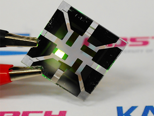
Figure 1: Application of Graphene-based OLEDs
This picture shows an OLED with the composite structure of TiO2/graphene/conducting polymer electrode in operation. The OLED exhibits 40.8% of ultrahigh external quantum efficiency (EQE) and 160.3 lm/W of power efficiency. The device prepared on a plastic substrate shown in the right remains intact and operates well even after 1,000 bending cycles at a radius of curvature as small as 2.3 mm.
Figure 2: Schematic Device Structure of Graphene-based OLEDs
This picture shows the new architecture to develop highly flexible OLEDs with excellent efficiency by using graphene as a transparent electrode (TE).
2016.06.07 View 15744
Graphene-Based Transparent Electrodes for Highly Efficient Flexible OLEDs
A Korean research team developed an ideal electrode structure composed of graphene and layers of titanium dioxide and conducting polymers, resulting in highly flexible and efficient OLEDs.
The arrival of a thin and lightweight computer that even rolls up like a piece of paper will not be in the far distant future. Flexible organic light-emitting diodes (OLEDs), built upon a plastic substrate, have received greater attention lately for their use in next-generation displays that can be bent or rolled while still operating.
A Korean research team led by Professor Seunghyup Yoo from the School of Electrical Engineering, KAIST and Professor Tae-Woo Lee from the Department of Materials Science and Engineering, Pohang University of Science and Technology (POSTECH) has developed highly flexible OLEDs with excellent efficiency by using graphene as a transparent electrode (TE) which is placed in between titanium dioxide (TiO2) and conducting polymer layers. The research results were published online on June 2, 2016 in Nature Communications.
OLEDs are stacked in several ultra-thin layers on glass, foil, or plastic substrates, in which multi-layers of organic compounds are sandwiched between two electrodes (cathode and anode). When voltage is applied across the electrodes, electrons from the cathode and holes (positive charges) from the anode draw toward each other and meet in the emissive layer. OLEDs emit light as an electron recombines with a positive hole, releasing energy in the form of a photon. One of the electrodes in OLEDs is usually transparent, and depending on which electrode is transparent, OLEDs can either emit from the top or bottom.
In conventional bottom-emission OLEDs, an anode is transparent in order for the emitted photons to exit the device through its substrate. Indium-tin-oxide (ITO) is commonly used as a transparent anode because of its high transparency, low sheet resistance, and well-established manufacturing process. However, ITO can potentially be expensive, and moreover, is brittle, being susceptible to bending-induced formation of cracks.
Graphene, a two-dimensional thin layer of carbon atoms tightly bonded together in a hexagonal honeycomb lattice, has recently emerged as an alternative to ITO. With outstanding electrical, physical, and chemical properties, its atomic thinness leading to a high degree of flexibility and transparency makes it an ideal candidate for TEs. Nonetheless, the efficiency of graphene-based OLEDs reported to date has been, at best, about the same level of ITO-based OLEDs.
As a solution, the Korean research team, which further includes Professors Sung-Yool Choi (Electrical Engineering) and Taek-Soo Kim (Mechanical Engineering) of KAIST and their students, proposed a new device architecture that can maximize the efficiency of graphene-based OLEDs. They fabricated a transparent anode in a composite structure in which a TiO2 layer with a high refractive index (high-n) and a hole-injection layer (HIL) of conducting polymers with a low refractive index (low-n) sandwich graphene electrodes. This is an optical design that induces a synergistic collaboration between the high-n and low-n layers to increase the effective reflectance of TEs. As a result, the enhancement of the optical cavity resonance is maximized. The optical cavity resonance is related to the improvement of efficiency and color gamut in OLEDs. At the same time, the loss from surface plasmon polariton (SPP), a major cause for weak photon emissions in OLEDs, is also reduced due to the presence of the low-n conducting polymers.
Under this approach, graphene-based OLEDs exhibit 40.8% of ultrahigh external quantum efficiency (EQE) and 160.3 lm/W of power efficiency, which is unprecedented in those using graphene as a TE. Furthermore, these devices remain intact and operate well even after 1,000 bending cycles at a radius of curvature as small as 2.3 mm. This is a remarkable result for OLEDs containing oxide layers such as TiO2 because oxides are typically brittle and prone to bending-induced fractures even at a relatively low strain. The research team discovered that TiO2 has a crack-deflection toughening mechanism that tends to prevent bending-induced cracks from being formed easily.
Professor Yoo said, “What’s unique and advanced about this technology, compared with previous graphene-based OLEDs, is the synergistic collaboration of high- and low-index layers that enables optical management of both resonance effect and SPP loss, leading to significant enhancement in efficiency, all with little compromise in flexibility.” He added, “Our work was the achievement of collaborative research, transcending the boundaries of different fields, through which we have often found meaningful breakthroughs.”
Professor Lee said, “We expect that our technology will pave the way to develop an OLED light source for highly flexible and wearable displays, or flexible sensors that can be attached to the human body for health monitoring, for instance.”
The research paper is entitled “Synergistic Electrode Architecture for Efficient Graphene-based Flexible Organic Light-emitting Diodes” (DOI. 10.1038/NCOMMS11791). The lead authors are Jae-Ho Lee, a Ph.D. candidate at KAIST; Tae-Hee Han, a Ph.D. researcher at POSTECH; and Min-Ho Park, a Ph.D. candidate at POSTECH.
This study was supported by the Basic Science Research Program of the National Research Foundation of Korea (NRF) through the Center for Advanced Flexible Display (CAFDC) funded by the Ministry of Science, ICT and Future Planning (MSIP); by the Center for Advanced Soft-Electronics funded by the MSIP as a Global Frontier Project; by the Graphene Research Center Program of KAIST; and by grants from the IT R&D Program of the Ministry of Trade, Industry and Energy of Korea (MOTIE).
Figure 1: Application of Graphene-based OLEDs
This picture shows an OLED with the composite structure of TiO2/graphene/conducting polymer electrode in operation. The OLED exhibits 40.8% of ultrahigh external quantum efficiency (EQE) and 160.3 lm/W of power efficiency. The device prepared on a plastic substrate shown in the right remains intact and operates well even after 1,000 bending cycles at a radius of curvature as small as 2.3 mm.
Figure 2: Schematic Device Structure of Graphene-based OLEDs
This picture shows the new architecture to develop highly flexible OLEDs with excellent efficiency by using graphene as a transparent electrode (TE).
2016.06.07 View 15744 -
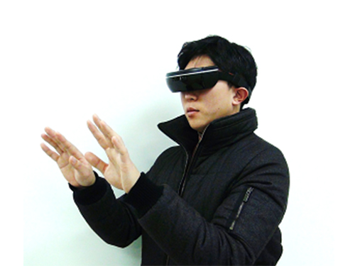 K-Glass 3 Offers Users a Keyboard to Type Text
KAIST researchers upgraded their smart glasses with a low-power multicore processor to employ stereo vision and deep-learning algorithms, making the user interface and experience more intuitive and convenient.
K-Glass, smart glasses reinforced with augmented reality (AR) that were first developed by KAIST in 2014, with the second version released in 2015, is back with an even stronger model. The latest version, which KAIST researchers are calling K-Glass 3, allows users to text a message or type in key words for Internet surfing by offering a virtual keyboard for text and even one for a piano.
Currently, most wearable head-mounted displays (HMDs) suffer from a lack of rich user interfaces, short battery lives, and heavy weight. Some HMDs, such as Google Glass, use a touch panel and voice commands as an interface, but they are considered merely an extension of smartphones and are not optimized for wearable smart glasses. Recently, gaze recognition was proposed for HMDs including K-Glass 2, but gaze cannot be realized as a natural user interface (UI) and experience (UX) due to its limited interactivity and lengthy gaze-calibration time, which can be up to several minutes.
As a solution, Professor Hoi-Jun Yoo and his team from the Electrical Engineering Department recently developed K-Glass 3 with a low-power natural UI and UX processor. This processor is composed of a pre-processing core to implement stereo vision, seven deep-learning cores to accelerate real-time scene recognition within 33 milliseconds, and one rendering engine for the display.
The stereo-vision camera, located on the front of K-Glass 3, works in a manner similar to three dimension (3D) sensing in human vision. The camera’s two lenses, displayed horizontally from one another just like depth perception produced by left and right eyes, take pictures of the same objects or scenes and combine these two different images to extract spatial depth information, which is necessary to reconstruct 3D environments. The camera’s vision algorithm has an energy efficiency of 20 milliwatts on average, allowing it to operate in the Glass more than 24 hours without interruption.
The research team adopted deep-learning-multi core technology dedicated for mobile devices. This technology has greatly improved the Glass’s recognition accuracy with images and speech, while shortening the time needed to process and analyze data. In addition, the Glass’s multi-core processor is advanced enough to become idle when it detects no motion from users. Instead, it executes complex deep-learning algorithms with a minimal power to achieve high performance.
Professor Yoo said, “We have succeeded in fabricating a low-power multi-core processer that consumes only 126 milliwatts of power with a high efficiency rate. It is essential to develop a smaller, lighter, and low-power processor if we want to incorporate the widespread use of smart glasses and wearable devices into everyday life. K-Glass 3’s more intuitive UI and convenient UX permit users to enjoy enhanced AR experiences such as a keyboard or a better, more responsive mouse.”
Along with the research team, UX Factory, a Korean UI and UX developer, participated in the K-Glass 3 project.
These research results entitled “A 126.1mW Real-Time Natural UI/UX Processor with Embedded Deep-Learning Core for Low-Power Smart Glasses” (lead author: Seong-Wook Park, a doctoral student in the Electrical Engineering Department, KAIST) were presented at the 2016 IEEE (Institute of Electrical and Electronics Engineers) International Solid-State Circuits Conference (ISSCC) that took place January 31-February 4, 2016 in San Francisco, California.
YouTube Link: https://youtu.be/If_anx5NerQ
Figure 1: K-Glass 3
K-Glass 3 is equipped with a stereo camera, dual microphones, a WiFi module, and eight batteries to offer higher recognition accuracy and enhanced augmented reality experiences than previous models.
Figure 2: Architecture of the Low-Power Multi-Core Processor
K-Glass 3’s processor is designed to include several cores for pre-processing, deep-learning, and graphic rendering.
Figure 3: Virtual Text and Piano Keyboard
K-Glass 3 can detect hands and recognize their movements to provide users with such augmented reality applications as a virtual text or piano keyboard.
2016.02.26 View 14545
K-Glass 3 Offers Users a Keyboard to Type Text
KAIST researchers upgraded their smart glasses with a low-power multicore processor to employ stereo vision and deep-learning algorithms, making the user interface and experience more intuitive and convenient.
K-Glass, smart glasses reinforced with augmented reality (AR) that were first developed by KAIST in 2014, with the second version released in 2015, is back with an even stronger model. The latest version, which KAIST researchers are calling K-Glass 3, allows users to text a message or type in key words for Internet surfing by offering a virtual keyboard for text and even one for a piano.
Currently, most wearable head-mounted displays (HMDs) suffer from a lack of rich user interfaces, short battery lives, and heavy weight. Some HMDs, such as Google Glass, use a touch panel and voice commands as an interface, but they are considered merely an extension of smartphones and are not optimized for wearable smart glasses. Recently, gaze recognition was proposed for HMDs including K-Glass 2, but gaze cannot be realized as a natural user interface (UI) and experience (UX) due to its limited interactivity and lengthy gaze-calibration time, which can be up to several minutes.
As a solution, Professor Hoi-Jun Yoo and his team from the Electrical Engineering Department recently developed K-Glass 3 with a low-power natural UI and UX processor. This processor is composed of a pre-processing core to implement stereo vision, seven deep-learning cores to accelerate real-time scene recognition within 33 milliseconds, and one rendering engine for the display.
The stereo-vision camera, located on the front of K-Glass 3, works in a manner similar to three dimension (3D) sensing in human vision. The camera’s two lenses, displayed horizontally from one another just like depth perception produced by left and right eyes, take pictures of the same objects or scenes and combine these two different images to extract spatial depth information, which is necessary to reconstruct 3D environments. The camera’s vision algorithm has an energy efficiency of 20 milliwatts on average, allowing it to operate in the Glass more than 24 hours without interruption.
The research team adopted deep-learning-multi core technology dedicated for mobile devices. This technology has greatly improved the Glass’s recognition accuracy with images and speech, while shortening the time needed to process and analyze data. In addition, the Glass’s multi-core processor is advanced enough to become idle when it detects no motion from users. Instead, it executes complex deep-learning algorithms with a minimal power to achieve high performance.
Professor Yoo said, “We have succeeded in fabricating a low-power multi-core processer that consumes only 126 milliwatts of power with a high efficiency rate. It is essential to develop a smaller, lighter, and low-power processor if we want to incorporate the widespread use of smart glasses and wearable devices into everyday life. K-Glass 3’s more intuitive UI and convenient UX permit users to enjoy enhanced AR experiences such as a keyboard or a better, more responsive mouse.”
Along with the research team, UX Factory, a Korean UI and UX developer, participated in the K-Glass 3 project.
These research results entitled “A 126.1mW Real-Time Natural UI/UX Processor with Embedded Deep-Learning Core for Low-Power Smart Glasses” (lead author: Seong-Wook Park, a doctoral student in the Electrical Engineering Department, KAIST) were presented at the 2016 IEEE (Institute of Electrical and Electronics Engineers) International Solid-State Circuits Conference (ISSCC) that took place January 31-February 4, 2016 in San Francisco, California.
YouTube Link: https://youtu.be/If_anx5NerQ
Figure 1: K-Glass 3
K-Glass 3 is equipped with a stereo camera, dual microphones, a WiFi module, and eight batteries to offer higher recognition accuracy and enhanced augmented reality experiences than previous models.
Figure 2: Architecture of the Low-Power Multi-Core Processor
K-Glass 3’s processor is designed to include several cores for pre-processing, deep-learning, and graphic rendering.
Figure 3: Virtual Text and Piano Keyboard
K-Glass 3 can detect hands and recognize their movements to provide users with such augmented reality applications as a virtual text or piano keyboard.
2016.02.26 View 14545 -
 A KAIST Student Donates USD 26,000 to His Alma Mater
A KAIST undergraduate student who developed and sold a smart phone application donated USD 26,000 to his alma mater.
Seung-Kyu Oh of the School of Electrical Engineering gave his donation to President Steve Kang of KAIST on November 24, 2015. This is the largest amount donated by an enrolled undergraduate.
In 2010, at a time when android smart phones were just being released, Mr. Oh decided to develop a subway app because existing subway apps were not user-friendly.
Mr. Oh’s “Subway Navigation” app checks the current operation hours and gives users the shortest path when the user selects points of departure and arrival. The calculation for the shortest path involves factors such as which train comes first, where and to what train to transfer, the first and last trains of the day, transfer passageway usage time, etc.
To make the app useful to the largest number of people, Mr. Oh distributed it on the open market. Currently, the app is ranked the second most downloaded subway app, and has even made considerable advertising profits, having accumulated more than 5,000,000 users. This year, Mr. Oh received an offer from Kakao, an Internet company based in Seoul, Korea, to take over the app and sold it to them.
Mr. Oh said that making a donation KAIST was the first thing that came to his mind when he earned this profit.
Mr. Oh, who graduated from the Korea Science Academy, a science magnet high school, said that he felt a sense of responsibility for receiving support from Korea since high school, and that he decided to donate to KAIST as a way of returning the support that he had received so far.
He further said that “if an individual’s efforts and talents created some profit together with what he or she learned from school, then the school that supported the student in furthering his studies has also played a significant role,” and that “likewise, our stellar alumni can contribute more to our younger classmates’ growth and development.”
Mr. Oh, who is at his last semester, plans to join Kakao and will take on a job managing his subway app.
President Kang said he hopes that “all KAISTians will emulate Mr. Oh’s example to support the school” and that “the university will use the money to invest further in its future.”
2015.11.24 View 5117
A KAIST Student Donates USD 26,000 to His Alma Mater
A KAIST undergraduate student who developed and sold a smart phone application donated USD 26,000 to his alma mater.
Seung-Kyu Oh of the School of Electrical Engineering gave his donation to President Steve Kang of KAIST on November 24, 2015. This is the largest amount donated by an enrolled undergraduate.
In 2010, at a time when android smart phones were just being released, Mr. Oh decided to develop a subway app because existing subway apps were not user-friendly.
Mr. Oh’s “Subway Navigation” app checks the current operation hours and gives users the shortest path when the user selects points of departure and arrival. The calculation for the shortest path involves factors such as which train comes first, where and to what train to transfer, the first and last trains of the day, transfer passageway usage time, etc.
To make the app useful to the largest number of people, Mr. Oh distributed it on the open market. Currently, the app is ranked the second most downloaded subway app, and has even made considerable advertising profits, having accumulated more than 5,000,000 users. This year, Mr. Oh received an offer from Kakao, an Internet company based in Seoul, Korea, to take over the app and sold it to them.
Mr. Oh said that making a donation KAIST was the first thing that came to his mind when he earned this profit.
Mr. Oh, who graduated from the Korea Science Academy, a science magnet high school, said that he felt a sense of responsibility for receiving support from Korea since high school, and that he decided to donate to KAIST as a way of returning the support that he had received so far.
He further said that “if an individual’s efforts and talents created some profit together with what he or she learned from school, then the school that supported the student in furthering his studies has also played a significant role,” and that “likewise, our stellar alumni can contribute more to our younger classmates’ growth and development.”
Mr. Oh, who is at his last semester, plans to join Kakao and will take on a job managing his subway app.
President Kang said he hopes that “all KAISTians will emulate Mr. Oh’s example to support the school” and that “the university will use the money to invest further in its future.”
2015.11.24 View 5117 -
 KAIST Hosts the Wearable Computer Contest 2015
“What you see is a compact electronic system on a dust mask, which monitors the amount of dust taken in by a worker and lets other workers know if the person is injured in an industrial site,” said Bum Taek Jung, a Master’s candidate from Sungkyunkwan University during the Wearable Computer Contest 2015 held in KI building of KAIST on November 5, 2015.
He explained his interest in developing this system, “Dust-related respiratory diseases and falling accidents are still prevalent in industrial sites.” He added, “Using the smart dust mask helps monitoring workers’ physical condition in real time, allowing us to cope with accidents in a much more timely manner.” A smart dust mask is a portable device that alerts the user with orange or red light signs when the amount of dust inhaled by the user is higher than the threshold. Its application on a smartphone can also allow project managers to alert the risk of falling accidents to workers by employing a gyroscope and an accelerometer on the mask.
The Wearable Computer Contest 2015 met for the eleventh time at KAIST on November 5-6, 2015. A wearable computer refers to a portable device which users can wear directly on the body or on their clothes while moving. Products that can provide various services by connecting to a smartphone have become increasingly popular. The contest is an excellent opportunity for university students to design creative wearable systems similar to those often depicted in movies and comics.
This year 102 teams from universities all over the nation participated. After screening and evaluation of their presentations, only 8 teams in the product section and 3 teams in the ideas section were selected for the finals. Of the many entries to the contest, the ECG security system caught many people’s attention. The wearable, which attaches to a shirt, acts like an electrocardiogram. By comparing the ECG reading with the one stored in the data server, the wearable can authenticate the user. The system could be widely used by enterprises and financial companies where tight security and authentication are crucial.
The winners of the product and the ideas sections received USD 4,300 and usd 860 respectively along with Minister Prizes from the Minister of Science, ICT and Future Planning of Korea. The Chairman of the contest, Professor Hoi-Jun Yoo from the Electrical Engineering Department of KAIST said, “The contest will be a great opportunity for anyone to have a look at advanced wearable devices developed through close integration of state-of-the-art technologies and creative ideas from young minds.”
2015.11.05 View 9874
KAIST Hosts the Wearable Computer Contest 2015
“What you see is a compact electronic system on a dust mask, which monitors the amount of dust taken in by a worker and lets other workers know if the person is injured in an industrial site,” said Bum Taek Jung, a Master’s candidate from Sungkyunkwan University during the Wearable Computer Contest 2015 held in KI building of KAIST on November 5, 2015.
He explained his interest in developing this system, “Dust-related respiratory diseases and falling accidents are still prevalent in industrial sites.” He added, “Using the smart dust mask helps monitoring workers’ physical condition in real time, allowing us to cope with accidents in a much more timely manner.” A smart dust mask is a portable device that alerts the user with orange or red light signs when the amount of dust inhaled by the user is higher than the threshold. Its application on a smartphone can also allow project managers to alert the risk of falling accidents to workers by employing a gyroscope and an accelerometer on the mask.
The Wearable Computer Contest 2015 met for the eleventh time at KAIST on November 5-6, 2015. A wearable computer refers to a portable device which users can wear directly on the body or on their clothes while moving. Products that can provide various services by connecting to a smartphone have become increasingly popular. The contest is an excellent opportunity for university students to design creative wearable systems similar to those often depicted in movies and comics.
This year 102 teams from universities all over the nation participated. After screening and evaluation of their presentations, only 8 teams in the product section and 3 teams in the ideas section were selected for the finals. Of the many entries to the contest, the ECG security system caught many people’s attention. The wearable, which attaches to a shirt, acts like an electrocardiogram. By comparing the ECG reading with the one stored in the data server, the wearable can authenticate the user. The system could be widely used by enterprises and financial companies where tight security and authentication are crucial.
The winners of the product and the ideas sections received USD 4,300 and usd 860 respectively along with Minister Prizes from the Minister of Science, ICT and Future Planning of Korea. The Chairman of the contest, Professor Hoi-Jun Yoo from the Electrical Engineering Department of KAIST said, “The contest will be a great opportunity for anyone to have a look at advanced wearable devices developed through close integration of state-of-the-art technologies and creative ideas from young minds.”
2015.11.05 View 9874