%41%74%6f%6d
-
 KAIST Develops Ultrafast Photothermal Process Achieving 3,000 °C in 0.02 Seconds, Boosting Hydrogen Production Efficiency Sixfold
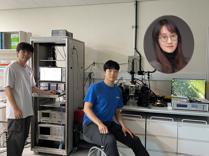
< (from left) Ph.D. candidate Seohak Park, Dr. Jaewan Ahn, Ph.D. candidate Dogyeong Jeon, Prof. Sung-Yool Choi, Prof. Il-Doo Kim, Dr. Chungseong Park, Ph.D. candidate Euichul Shin (top left) Dr. Hamin Shin, Dr. Jun-Hwe Cha i>
The rapid and energy-efficient synthesis of high-performance catalysts is a critical hurdle in advancing clean energy technologies like hydrogen production. Addressing this challenge, a research team at KAIST has now developed a novel platform technology that utilizes a 0.02-second flash of light to generate an ultrahigh temperature of 3,000 °C, enabling the highly efficient synthesis of catalysts. This breakthrough process reduces energy consumption by more than a thousandfold compared to conventional methods while increasing hydrogen production efficiency by up to six times, marking a significant step toward the commercialization of clean energy.
KAIST (President Kwang Hyung Lee) announced on October 20 that a joint research team, co-led by Professor Il-Doo Kim from the Department of Materials Science and Engineering and Professor Sung-Yool Choi from the School of Electrical Engineering, has developed a “direct-contact photothermal annealing” platform. This technique synthesizes high-performance nanomaterials through brief exposure to intense light, generating a transient temperature of 3,000 °C in just 0.02 seconds.
Using this intense photothermal energy, the researchers successfully converted chemically inert nanodiamond (ND) precursors into highly conductive and catalytically active carbon nanoonions (CNOs).
More impressively, the method simultaneously functionalizes the surface of the newly formed CNOs with single atoms. This integrated, one-step process restructures the support material and embeds catalytic functionality in a single light pulse, representing a significant innovation in catalyst synthesis.
CNOs, composed of concentric graphitic shells, are ideal catalyst supports due to their high conductivity, large specific surface area, and chemical stability. However, traditional CNO synthesis has been hindered by complex, multi-step post-processing required to load metal catalysts and by reliance on energy-intensive, time-consuming thermal treatments that limit scalability.
< Schematic Illustration of the Limitations of Conventional Thermal-Radiation Synthesis and the Carbon Nano-Onion Conversion via Direct-Contact Photothermal Treatment >
To overcome these limitations, the KAIST team leveraged the photothermal effect. They devised a method of mixing ND precursors with light-absorbing carbon black (CB) and applying an intense pulse from a xenon lamp. This approach triggers the transformation of NDs into CNOs in just 0.02 seconds, a phenomenon validated by molecular dynamics simulations.
A key innovation of this platform is the simultaneous synthesis of CNOs and functionalization of single-atom catalysts (SACs). When metal precursors, such as platinum (Pt), are included in the mixture, they decompose and anchor onto the surface of the nascent CNOs as individual atoms. The subsequent rapid cooling prevents atomic aggregation, resulting in a perfectly integrated one-step process for both synthesis and functionalization. The team has successfully synthesized eight different high-density SACs, including platinum (Pt), cobalt (Co), and nickel (Ni). The resulting Pt-CNO demonstrated a sixfold enhancement in hydrogen evolution efficiency compared to conventional catalysts, achieving high performance with significantly smaller quantities of precious metals. This highlights the technology's potential for scalable and sustainable hydrogen production.
“We have developed, for the first time, a direct-contact photothermal annealing process that reaches 3,000°C in under 0.02 seconds,” said Professor Il-Doo Kim. “This ultrafast synthesis and single-atom functionalization platform reduces energy consumption by more than a thousandfold compared to traditional methods. We expect it to accelerate the commercialization of technologies in hydrogen energy, gas sensing, and environmental catalysis.”
The study’s first authors are Dogyeong Jeon (Ph.D. candidate, Department of Materials Science and Engineering, KAIST), Dr. Hamin Shin (an alumnus of the Department of Materials Science and Engineering and a current postdoctoral researcher at ETH Zurich), and Dr. Jun-Hwe Cha (an alumnus of the School of Electrical Engineering, now at SK hynix). Professors Sung-Yool Choi and Il-Doo Kim are the corresponding authors.\
< Inside Cover Image of the September Issue of ACS >
The research was published as a Supplementary Cover Article in the September issue of ACS Nano, a leading international journal of the American Chemical Society (ACS).
※ Paper title: “Photothermal Annealing-Enabled Millisecond Synthesis of Carbon Nanoonions and Simultaneous Single-Atom Functionalization,” DOI: 10.1021/acsnano.5c11229
This research was supported by the Global R&D Infrastructure Program and the Leading Research Center Program of the National Research Foundation of Korea (NRF), funded by the Ministry of Science and ICT, and the Nano Convergence Technology Center’s Semiconductor–Battery Interfacing Platform Development Project.
2025.10.21 View 2947
KAIST Develops Ultrafast Photothermal Process Achieving 3,000 °C in 0.02 Seconds, Boosting Hydrogen Production Efficiency Sixfold
< (from left) Ph.D. candidate Seohak Park, Dr. Jaewan Ahn, Ph.D. candidate Dogyeong Jeon, Prof. Sung-Yool Choi, Prof. Il-Doo Kim, Dr. Chungseong Park, Ph.D. candidate Euichul Shin (top left) Dr. Hamin Shin, Dr. Jun-Hwe Cha i>
The rapid and energy-efficient synthesis of high-performance catalysts is a critical hurdle in advancing clean energy technologies like hydrogen production. Addressing this challenge, a research team at KAIST has now developed a novel platform technology that utilizes a 0.02-second flash of light to generate an ultrahigh temperature of 3,000 °C, enabling the highly efficient synthesis of catalysts. This breakthrough process reduces energy consumption by more than a thousandfold compared to conventional methods while increasing hydrogen production efficiency by up to six times, marking a significant step toward the commercialization of clean energy.
KAIST (President Kwang Hyung Lee) announced on October 20 that a joint research team, co-led by Professor Il-Doo Kim from the Department of Materials Science and Engineering and Professor Sung-Yool Choi from the School of Electrical Engineering, has developed a “direct-contact photothermal annealing” platform. This technique synthesizes high-performance nanomaterials through brief exposure to intense light, generating a transient temperature of 3,000 °C in just 0.02 seconds.
Using this intense photothermal energy, the researchers successfully converted chemically inert nanodiamond (ND) precursors into highly conductive and catalytically active carbon nanoonions (CNOs).
More impressively, the method simultaneously functionalizes the surface of the newly formed CNOs with single atoms. This integrated, one-step process restructures the support material and embeds catalytic functionality in a single light pulse, representing a significant innovation in catalyst synthesis.
CNOs, composed of concentric graphitic shells, are ideal catalyst supports due to their high conductivity, large specific surface area, and chemical stability. However, traditional CNO synthesis has been hindered by complex, multi-step post-processing required to load metal catalysts and by reliance on energy-intensive, time-consuming thermal treatments that limit scalability.
< Schematic Illustration of the Limitations of Conventional Thermal-Radiation Synthesis and the Carbon Nano-Onion Conversion via Direct-Contact Photothermal Treatment >
To overcome these limitations, the KAIST team leveraged the photothermal effect. They devised a method of mixing ND precursors with light-absorbing carbon black (CB) and applying an intense pulse from a xenon lamp. This approach triggers the transformation of NDs into CNOs in just 0.02 seconds, a phenomenon validated by molecular dynamics simulations.
A key innovation of this platform is the simultaneous synthesis of CNOs and functionalization of single-atom catalysts (SACs). When metal precursors, such as platinum (Pt), are included in the mixture, they decompose and anchor onto the surface of the nascent CNOs as individual atoms. The subsequent rapid cooling prevents atomic aggregation, resulting in a perfectly integrated one-step process for both synthesis and functionalization. The team has successfully synthesized eight different high-density SACs, including platinum (Pt), cobalt (Co), and nickel (Ni). The resulting Pt-CNO demonstrated a sixfold enhancement in hydrogen evolution efficiency compared to conventional catalysts, achieving high performance with significantly smaller quantities of precious metals. This highlights the technology's potential for scalable and sustainable hydrogen production.
“We have developed, for the first time, a direct-contact photothermal annealing process that reaches 3,000°C in under 0.02 seconds,” said Professor Il-Doo Kim. “This ultrafast synthesis and single-atom functionalization platform reduces energy consumption by more than a thousandfold compared to traditional methods. We expect it to accelerate the commercialization of technologies in hydrogen energy, gas sensing, and environmental catalysis.”
The study’s first authors are Dogyeong Jeon (Ph.D. candidate, Department of Materials Science and Engineering, KAIST), Dr. Hamin Shin (an alumnus of the Department of Materials Science and Engineering and a current postdoctoral researcher at ETH Zurich), and Dr. Jun-Hwe Cha (an alumnus of the School of Electrical Engineering, now at SK hynix). Professors Sung-Yool Choi and Il-Doo Kim are the corresponding authors.\
< Inside Cover Image of the September Issue of ACS >
The research was published as a Supplementary Cover Article in the September issue of ACS Nano, a leading international journal of the American Chemical Society (ACS).
※ Paper title: “Photothermal Annealing-Enabled Millisecond Synthesis of Carbon Nanoonions and Simultaneous Single-Atom Functionalization,” DOI: 10.1021/acsnano.5c11229
This research was supported by the Global R&D Infrastructure Program and the Leading Research Center Program of the National Research Foundation of Korea (NRF), funded by the Ministry of Science and ICT, and the Nano Convergence Technology Center’s Semiconductor–Battery Interfacing Platform Development Project.
2025.10.21 View 2947 -
 First Elucidation of Spontaneous Emission and Excitation in Photonic Time Crystals
< (From left) Professor Bumki Min, Ph.D. Candidate Kyungmin Lee >
A groundbreaking discovery reveals that spontaneous emission, a key phenomenon in the interaction between light and atoms, manifests in a new form within a Photonic Time Crystal (PTC). This research, led by a KAIST team, not only overturns existing theory but further predicts a novel phenomenon: spontaneous emission excitation.
Professor Bumki Min's research team from the KAIST Department of Physics, in collaboration with Professor Jonghwa Shin of the Department of Materials Science and Engineering, Professor Wonju Jeon of the Department of Mechanical Engineering, Professor Gil Young Cho of the Department of Physics, and researchers from IBS, UC Berkeley, and the Hong Kong University of Science and Technology, announced that they have proven that the spontaneous emission decay rate in a Photonic Time Crystal is, on the contrary, enhanced rather than being "extinguished," as suggested by a paper published in Science in 2022. Furthermore, they predicted a new process—spontaneous emission excitation—where an atom transitions from its ground state to an excited state while simultaneously emitting a photon.
< Spontaneous emission decay rate (left) and spontaneous emission excitation rate (right) when a quantum emitter (or atom) is placed in an environment that changes very rapidly and periodically in time >
Spontaneous emission is the process by which an atom intrinsically emits a photon and is fundamental to quantum optics and photonic device research. Until now, control over spontaneous emission has been achieved by designing spatial structures like resonators or photonic crystals. However, the advent of Photonic Time Crystals, which periodically modulate the refractive index of a medium over time, has drawn attention to the potential for control along the time axis.
Previous theory predicted that the spontaneous emission decay rate in a Photonic Time Crystal would completely vanish at a specific frequency. In contrast, this study is the first to prove that the decay rate is significantly enhanced. This is attributed to the non-orthogonal mode effect, highlighting the importance of research into non-Hermitian optics.
The research team also predicted and reported a new process, 'spontaneous emission excitation,' where an atom gains energy and transitions from its ground state to an excited state while simultaneously emitting a photon. This is a non-equilibrium process made possible by the time-crystal medium supplying external energy, representing a new light-matter interaction phenomenon that cannot be explained by conventional equilibrium optics.
The findings fundamentally shift the paradigm of spontaneous emission research and hold promise for broad applications in fields such as quantum light source design and non-equilibrium quantum optics.
Professor Bumki Min stated, "This achievement re-establishes the fundamental theory describing spontaneous emission in a rapidly time-varying environment. The enhancement of spontaneous emission decay and the 'spontaneous emission excitation' phenomenon have the potential to change the paradigm of light-matter interaction research."
Ph.D. candidate Kyungmin Lee participated as the first author of this research. The results were published online in the international academic journal Physical Review Letters on September 23, 2025, simultaneously highlighted on Physics.org, and selected as an Editors' Suggestion paper. The research was supported by the National Research Foundation of Korea and the Samsung Science and Technology Foundation.
Note: The paper is titled “Spontaneous emission decay and excitation in photonic time crystals.”
2025.10.01 View 2680
First Elucidation of Spontaneous Emission and Excitation in Photonic Time Crystals
< (From left) Professor Bumki Min, Ph.D. Candidate Kyungmin Lee >
A groundbreaking discovery reveals that spontaneous emission, a key phenomenon in the interaction between light and atoms, manifests in a new form within a Photonic Time Crystal (PTC). This research, led by a KAIST team, not only overturns existing theory but further predicts a novel phenomenon: spontaneous emission excitation.
Professor Bumki Min's research team from the KAIST Department of Physics, in collaboration with Professor Jonghwa Shin of the Department of Materials Science and Engineering, Professor Wonju Jeon of the Department of Mechanical Engineering, Professor Gil Young Cho of the Department of Physics, and researchers from IBS, UC Berkeley, and the Hong Kong University of Science and Technology, announced that they have proven that the spontaneous emission decay rate in a Photonic Time Crystal is, on the contrary, enhanced rather than being "extinguished," as suggested by a paper published in Science in 2022. Furthermore, they predicted a new process—spontaneous emission excitation—where an atom transitions from its ground state to an excited state while simultaneously emitting a photon.
< Spontaneous emission decay rate (left) and spontaneous emission excitation rate (right) when a quantum emitter (or atom) is placed in an environment that changes very rapidly and periodically in time >
Spontaneous emission is the process by which an atom intrinsically emits a photon and is fundamental to quantum optics and photonic device research. Until now, control over spontaneous emission has been achieved by designing spatial structures like resonators or photonic crystals. However, the advent of Photonic Time Crystals, which periodically modulate the refractive index of a medium over time, has drawn attention to the potential for control along the time axis.
Previous theory predicted that the spontaneous emission decay rate in a Photonic Time Crystal would completely vanish at a specific frequency. In contrast, this study is the first to prove that the decay rate is significantly enhanced. This is attributed to the non-orthogonal mode effect, highlighting the importance of research into non-Hermitian optics.
The research team also predicted and reported a new process, 'spontaneous emission excitation,' where an atom gains energy and transitions from its ground state to an excited state while simultaneously emitting a photon. This is a non-equilibrium process made possible by the time-crystal medium supplying external energy, representing a new light-matter interaction phenomenon that cannot be explained by conventional equilibrium optics.
The findings fundamentally shift the paradigm of spontaneous emission research and hold promise for broad applications in fields such as quantum light source design and non-equilibrium quantum optics.
Professor Bumki Min stated, "This achievement re-establishes the fundamental theory describing spontaneous emission in a rapidly time-varying environment. The enhancement of spontaneous emission decay and the 'spontaneous emission excitation' phenomenon have the potential to change the paradigm of light-matter interaction research."
Ph.D. candidate Kyungmin Lee participated as the first author of this research. The results were published online in the international academic journal Physical Review Letters on September 23, 2025, simultaneously highlighted on Physics.org, and selected as an Editors' Suggestion paper. The research was supported by the National Research Foundation of Korea and the Samsung Science and Technology Foundation.
Note: The paper is titled “Spontaneous emission decay and excitation in photonic time crystals.”
2025.10.01 View 2680 -
 Tracking Atoms during Fuel Cell Cycles: KAIST Team Reveals the Atomic-Scale Secret Behind Fuel Cell Catalyst Durability
<Professor Yongsoo Yang, Professor Eun-Ae Cho, Dr. Chaehwa Jeong, Dr. Joohyuk Lee, Dr. Hyesung Cho, Researcher Kwangho Lee from KAIST>
Hydrogen fuel cell vehicles have long been hailed as the future of clean mobility: cars that emit nothing but water while delivering high efficiency and power density. Yet a stubborn obstacle remains. The heart of the fuel cell, the platinum-based catalyst, is both expensive and prone to degradation. Over time, the catalyst deteriorates during operation, forcing frequent replacements and keeping hydrogen vehicles costly.
Understanding why and how these catalysts degrade at the atomic level is a longstanding challenge in the catalysis research. Without this knowledge, designing truly durable and affordable fuel cells for mass adoption remains out of reach.
Now, a team led by Professor Yongsoo Yang of the Department of Physics at KAIST (Korea Advanced Institute of Science and Technology), in collaboration with Professor Eun-Ae Cho of KAIST’s Department of Materials Science and Engineering, researchers at Stanford University and the Lawrence Berkeley National Laboratory, has successfully tracked the three-dimensional change of individual atoms inside fuel cell catalysts during thousands of operating cycles. The results provide unprecedented insight into the atomic-scale degradation mechanisms of platinum-nickel (PtNi) catalysts, and demonstrate how gallium (Ga) doping dramatically improves both their performance and durability.
A New Atomic “CT Scan” for Catalysts
To achieve this breakthrough, the team utilized a neural network-assisted atomic electron tomography (AET) technique. Much like a CT scan in a hospital reconstructs the inside of the human body from X-ray images, AET determines the positions of thousands of atoms inside nanomaterials from high-resolution electron microscopy images taken at many different angles. By combining these reconstructions with advanced AI-based data correction, the researchers were able to map the exact 3D coordinates and chemical identity of every atom in the nanoparticle catalysts.
This allowed them to directly observe—at single-atom resolution—how the catalysts changed in structure, chemical composition, and internal strain as they were cycled thousands of times under fuel cell operating conditions.
Key Findings: Why Gallium Makes a Difference
The researchers compared conventional PtNi catalysts with Ga-doped PtNi catalysts. The results revealed:
a) Shape stability: While undoped PtNi particles gradually lost their advantageous octahedral shape and became more spherical (i.e., the fraction of highly active {111} facets has been reduced), Ga-doped particles retained their octahedral shape even after 12,000 cycles.
b) Chemical stability: In PtNi catalysts, nickel atoms leached from both the surface and subsurface regions, driving structural instability. In Ga-doped catalysts, surface nickel was largely preserved, preventing collapse of the structure.
c) Strain preservation: The compressive strain in PtNi particles, crucial for optimizing oxygen reduction activity, relaxed substantially over time. In contrast, Ga-doped particles maintained near-optimal strain.
d) Catalytic performance: By integrating these factors, the researchers showed that while undoped PtNi catalysts lost ~17% of their oxygen reduction activity after 12,000 cycles, Ga-doped PtNi catalysts lost only ~4% and maintained superior activity throughout.
Dr. Yang, who led the research, explained the significance of the results: “These results represent the first time the true 3D atomic-scale degradation dynamics of fuel cell catalysts have been directly visualized. Our findings not only reveal why gallium doping works, but also establish a powerful framework for rationally designing durable, high-efficiency catalysts.”
Implications for a Hydrogen-Powered Future
The study demonstrates that neural network-assisted AET can reveal how nanomaterials evolve during real operating conditions, overcoming the limitations of traditional 2D imaging and ensemble-averaged methods. Beyond PtNi catalysts, the technique can be applied to a wide range of nanomaterials and catalytic systems, helping to design the next generation of energy materials with atomic precision.
For the hydrogen economy, this means that more durable catalysts could extend the lifetime of fuel cells, lower replacement costs, and accelerate the widespread adoption of hydrogen-powered vehicles and clean energy technologies.
[Figure 1] Three-dimensional atomic structures and catalytic activity of Ga-doped PtNi nanoparticles during potential cycling. The top row shows the 3D atomic structures at different stages (Pristine to 12,000 cycles; blue: platinum, pink: nickel). The bottom row visualizes oxygen reduction reaction (ORR) catalytic activity, where red indicates higher activity. Gallium doping stabilizes the octahedral geometry and preserves highly active {111} facets, enabling sustained catalytic performance even after extensive cycling.
This research, with Chaehwa Jeong, Juhyeok Lee, Hyesung Jo, KwangHo Lee from the KAIST as co-first authors, was published online in Nature Communications on August 28th (Title: Atomic-scale 3D structural dynamics and functional degradation of Pt alloy nanocatalysts during the oxygen reduction reaction).
The study was mainly supported by the National Research Foundation of Korea (NRF) Grants funded by the Korean Government (MSIT).
2025.09.15 View 2658
Tracking Atoms during Fuel Cell Cycles: KAIST Team Reveals the Atomic-Scale Secret Behind Fuel Cell Catalyst Durability
<Professor Yongsoo Yang, Professor Eun-Ae Cho, Dr. Chaehwa Jeong, Dr. Joohyuk Lee, Dr. Hyesung Cho, Researcher Kwangho Lee from KAIST>
Hydrogen fuel cell vehicles have long been hailed as the future of clean mobility: cars that emit nothing but water while delivering high efficiency and power density. Yet a stubborn obstacle remains. The heart of the fuel cell, the platinum-based catalyst, is both expensive and prone to degradation. Over time, the catalyst deteriorates during operation, forcing frequent replacements and keeping hydrogen vehicles costly.
Understanding why and how these catalysts degrade at the atomic level is a longstanding challenge in the catalysis research. Without this knowledge, designing truly durable and affordable fuel cells for mass adoption remains out of reach.
Now, a team led by Professor Yongsoo Yang of the Department of Physics at KAIST (Korea Advanced Institute of Science and Technology), in collaboration with Professor Eun-Ae Cho of KAIST’s Department of Materials Science and Engineering, researchers at Stanford University and the Lawrence Berkeley National Laboratory, has successfully tracked the three-dimensional change of individual atoms inside fuel cell catalysts during thousands of operating cycles. The results provide unprecedented insight into the atomic-scale degradation mechanisms of platinum-nickel (PtNi) catalysts, and demonstrate how gallium (Ga) doping dramatically improves both their performance and durability.
A New Atomic “CT Scan” for Catalysts
To achieve this breakthrough, the team utilized a neural network-assisted atomic electron tomography (AET) technique. Much like a CT scan in a hospital reconstructs the inside of the human body from X-ray images, AET determines the positions of thousands of atoms inside nanomaterials from high-resolution electron microscopy images taken at many different angles. By combining these reconstructions with advanced AI-based data correction, the researchers were able to map the exact 3D coordinates and chemical identity of every atom in the nanoparticle catalysts.
This allowed them to directly observe—at single-atom resolution—how the catalysts changed in structure, chemical composition, and internal strain as they were cycled thousands of times under fuel cell operating conditions.
Key Findings: Why Gallium Makes a Difference
The researchers compared conventional PtNi catalysts with Ga-doped PtNi catalysts. The results revealed:
a) Shape stability: While undoped PtNi particles gradually lost their advantageous octahedral shape and became more spherical (i.e., the fraction of highly active {111} facets has been reduced), Ga-doped particles retained their octahedral shape even after 12,000 cycles.
b) Chemical stability: In PtNi catalysts, nickel atoms leached from both the surface and subsurface regions, driving structural instability. In Ga-doped catalysts, surface nickel was largely preserved, preventing collapse of the structure.
c) Strain preservation: The compressive strain in PtNi particles, crucial for optimizing oxygen reduction activity, relaxed substantially over time. In contrast, Ga-doped particles maintained near-optimal strain.
d) Catalytic performance: By integrating these factors, the researchers showed that while undoped PtNi catalysts lost ~17% of their oxygen reduction activity after 12,000 cycles, Ga-doped PtNi catalysts lost only ~4% and maintained superior activity throughout.
Dr. Yang, who led the research, explained the significance of the results: “These results represent the first time the true 3D atomic-scale degradation dynamics of fuel cell catalysts have been directly visualized. Our findings not only reveal why gallium doping works, but also establish a powerful framework for rationally designing durable, high-efficiency catalysts.”
Implications for a Hydrogen-Powered Future
The study demonstrates that neural network-assisted AET can reveal how nanomaterials evolve during real operating conditions, overcoming the limitations of traditional 2D imaging and ensemble-averaged methods. Beyond PtNi catalysts, the technique can be applied to a wide range of nanomaterials and catalytic systems, helping to design the next generation of energy materials with atomic precision.
For the hydrogen economy, this means that more durable catalysts could extend the lifetime of fuel cells, lower replacement costs, and accelerate the widespread adoption of hydrogen-powered vehicles and clean energy technologies.
[Figure 1] Three-dimensional atomic structures and catalytic activity of Ga-doped PtNi nanoparticles during potential cycling. The top row shows the 3D atomic structures at different stages (Pristine to 12,000 cycles; blue: platinum, pink: nickel). The bottom row visualizes oxygen reduction reaction (ORR) catalytic activity, where red indicates higher activity. Gallium doping stabilizes the octahedral geometry and preserves highly active {111} facets, enabling sustained catalytic performance even after extensive cycling.
This research, with Chaehwa Jeong, Juhyeok Lee, Hyesung Jo, KwangHo Lee from the KAIST as co-first authors, was published online in Nature Communications on August 28th (Title: Atomic-scale 3D structural dynamics and functional degradation of Pt alloy nanocatalysts during the oxygen reduction reaction).
The study was mainly supported by the National Research Foundation of Korea (NRF) Grants funded by the Korean Government (MSIT).
2025.09.15 View 2658 -
 KAIST Unlocks the Secret of Next-Generation Memory
<(From Left) Professor Sang-Hee Ko Park, Ph.D candidate Sunghwan Park, Ph.D candidate Chaewon Gong, Professor Seungbum Hong>
Resistive Random Access Memory (ReRAM), which is based on oxide materials, is gaining attention as a next-generation memory and neuromorphic computing device. Its fast speeds, data retention ability, and simple structure make it a promising candidate to replace existing memory technologies. KAIST researchers have now clarified the operating principle of this memory, which is expected to provide a key clue for the development of high-performance, high-reliability next-generation memory.
KAIST (President Kwang Hyung Lee) announced on the 2nd of September that a research team led by Professor Seungbum Hong from the Department of Materials Science and Engineering, in collaboration with a research team led by Professor Sang-Hee Ko Park from the same department, has for the first time in the world precisely clarified the operating principle of an oxide-based memory device, which is drawing attention as a core technology for next-generation semiconductors.
Using a 'Multi-modal Scanning Probe Microscope (Multi-modal SPM)' that combines several types of microscopes*, the research team succeeded in simultaneously observing the electron flow channels inside the oxide thin film, the movement of oxygen ions, and changes in surface potential (the distribution of charge on the material's surface). Through this, they clarified the correlation between how current changes and how oxygen defects change during the process of writing and erasing information in the memory.
*Several types of microscopes: Conductive atomic force microscopy (C-AFM) for observing current flow, electrochemical strain microscopy (ESM) for observing oxygen ion movement, and Kelvin probe force microscopy (KPFM) for observing potential changes.
With this special equipment, the research team directly implemented the process of writing and erasing information in the memory by applying an electrical signal to a titanium dioxide (TiO2) thin film, confirming at the nano-level that the reason for the current changes was the variation in the distribution of oxygen defects.
In this process, they confirmed that the current flow changes depending on the amount and location of oxygen defects. For example, when there are more oxygen defects, the electron pathway widens, and the current flows well, but conversely, when they scatter, the current is blocked. Through this, they succeeded in precisely visualizing that the distribution of oxygen defects within the oxide determines the on/off state of the memory.
<Overview of the Research Process. By using one of the SPM modes, C-AFM (Conductive Atomic Force Microscopy), resistive switching corresponding to the electroforming and reset processes is induced in a 10 nm-thick TiO₂ thin film, and the resulting local current variations caused by the applied electric field are observed. Subsequently, at the same location, ESM (Electrochemical Strain Microscopy) and KPFM (Kelvin Probe Force Microscopy) signals are comprehensively analyzed to investigate and interpret the spatial correlation of ion-electronic behaviors that influence the resistive switching phenomenon>
This research was not limited to the distribution at a single point but comprehensively analyzed the changes in current flow, the movement of oxygen ions, and the surface potential distribution after applying an electrical signal over a wide area of several square micrometers (µm2). As a result, they clarified that the process of the memory's resistance changing is not solely due to oxygen defects but is also closely intertwined with the movement of electrons (electronic behavior).
In particular, the research team confirmed that when oxygen ions are injected during the 'erasing process (reset process)', the memory can stably maintain its off state (high resistance state) for a long time. This is a core principle for increasing the reliability of memory devices and is expected to provide an important clue for the future development of stable, next-generation non-volatile memory.
Professor Seungbum Hong of KAIST, who led the research, said, "This is an example that proves we can directly observe the spatial correlation of oxygen defects, ions, and electrons through a multi-modal microscope." He added, "It is expected that this analysis technique will open a new chapter in the research and development of various metal oxide-based next-generation semiconductor devices in the future."
<By combining C-AFM and ESM techniques, the correlation between local conductivity and variations in oxygen vacancy concentration after resistive switching is analyzed. After the electroforming process, regions with increased conductivity exhibit an enhancement in the ESM amplitude signal, which can be interpreted as an increase in defect ion concentration. Conversely, after the reset process, regions with reduced conductivity show a corresponding decrease in this signal. Through these observations, it is spatially demonstrated that changes in conductivity and local defect ion concentration after resistive switching exhibit a positive correlation>
This research, in which Ph.D. candidate Chaewon Gong from the KAIST Department of Materials Science and Engineering participated as the first author, was published on July 20 in 'ACS Applied Materials and Interfaces', a prestigious academic journal in the field of new materials and chemical engineering published by the American Chemical Society (ACS).
※ Paper Title: Spatially Correlated Oxygen Vacancies, Electrons and Conducting Paths in TiO2 Thin Films
This research was carried out with the support of the Ministry of Science and ICT and the National Research Foundation of Korea.
2025.09.02 View 2810
KAIST Unlocks the Secret of Next-Generation Memory
<(From Left) Professor Sang-Hee Ko Park, Ph.D candidate Sunghwan Park, Ph.D candidate Chaewon Gong, Professor Seungbum Hong>
Resistive Random Access Memory (ReRAM), which is based on oxide materials, is gaining attention as a next-generation memory and neuromorphic computing device. Its fast speeds, data retention ability, and simple structure make it a promising candidate to replace existing memory technologies. KAIST researchers have now clarified the operating principle of this memory, which is expected to provide a key clue for the development of high-performance, high-reliability next-generation memory.
KAIST (President Kwang Hyung Lee) announced on the 2nd of September that a research team led by Professor Seungbum Hong from the Department of Materials Science and Engineering, in collaboration with a research team led by Professor Sang-Hee Ko Park from the same department, has for the first time in the world precisely clarified the operating principle of an oxide-based memory device, which is drawing attention as a core technology for next-generation semiconductors.
Using a 'Multi-modal Scanning Probe Microscope (Multi-modal SPM)' that combines several types of microscopes*, the research team succeeded in simultaneously observing the electron flow channels inside the oxide thin film, the movement of oxygen ions, and changes in surface potential (the distribution of charge on the material's surface). Through this, they clarified the correlation between how current changes and how oxygen defects change during the process of writing and erasing information in the memory.
*Several types of microscopes: Conductive atomic force microscopy (C-AFM) for observing current flow, electrochemical strain microscopy (ESM) for observing oxygen ion movement, and Kelvin probe force microscopy (KPFM) for observing potential changes.
With this special equipment, the research team directly implemented the process of writing and erasing information in the memory by applying an electrical signal to a titanium dioxide (TiO2) thin film, confirming at the nano-level that the reason for the current changes was the variation in the distribution of oxygen defects.
In this process, they confirmed that the current flow changes depending on the amount and location of oxygen defects. For example, when there are more oxygen defects, the electron pathway widens, and the current flows well, but conversely, when they scatter, the current is blocked. Through this, they succeeded in precisely visualizing that the distribution of oxygen defects within the oxide determines the on/off state of the memory.
<Overview of the Research Process. By using one of the SPM modes, C-AFM (Conductive Atomic Force Microscopy), resistive switching corresponding to the electroforming and reset processes is induced in a 10 nm-thick TiO₂ thin film, and the resulting local current variations caused by the applied electric field are observed. Subsequently, at the same location, ESM (Electrochemical Strain Microscopy) and KPFM (Kelvin Probe Force Microscopy) signals are comprehensively analyzed to investigate and interpret the spatial correlation of ion-electronic behaviors that influence the resistive switching phenomenon>
This research was not limited to the distribution at a single point but comprehensively analyzed the changes in current flow, the movement of oxygen ions, and the surface potential distribution after applying an electrical signal over a wide area of several square micrometers (µm2). As a result, they clarified that the process of the memory's resistance changing is not solely due to oxygen defects but is also closely intertwined with the movement of electrons (electronic behavior).
In particular, the research team confirmed that when oxygen ions are injected during the 'erasing process (reset process)', the memory can stably maintain its off state (high resistance state) for a long time. This is a core principle for increasing the reliability of memory devices and is expected to provide an important clue for the future development of stable, next-generation non-volatile memory.
Professor Seungbum Hong of KAIST, who led the research, said, "This is an example that proves we can directly observe the spatial correlation of oxygen defects, ions, and electrons through a multi-modal microscope." He added, "It is expected that this analysis technique will open a new chapter in the research and development of various metal oxide-based next-generation semiconductor devices in the future."
<By combining C-AFM and ESM techniques, the correlation between local conductivity and variations in oxygen vacancy concentration after resistive switching is analyzed. After the electroforming process, regions with increased conductivity exhibit an enhancement in the ESM amplitude signal, which can be interpreted as an increase in defect ion concentration. Conversely, after the reset process, regions with reduced conductivity show a corresponding decrease in this signal. Through these observations, it is spatially demonstrated that changes in conductivity and local defect ion concentration after resistive switching exhibit a positive correlation>
This research, in which Ph.D. candidate Chaewon Gong from the KAIST Department of Materials Science and Engineering participated as the first author, was published on July 20 in 'ACS Applied Materials and Interfaces', a prestigious academic journal in the field of new materials and chemical engineering published by the American Chemical Society (ACS).
※ Paper Title: Spatially Correlated Oxygen Vacancies, Electrons and Conducting Paths in TiO2 Thin Films
This research was carried out with the support of the Ministry of Science and ICT and the National Research Foundation of Korea.
2025.09.02 View 2810 -
 KAIST Takes the Lead in Developing Core Technologies for Generative AI National R&D Project
KAIST announced on the 15th of August that Professor Sanghoo Park of the Department of Nuclear and Quantum Engineering has won two consecutive awards for early-career researchers at two of the world's most prestigious plasma academic conferences.
Professor Park was selected as a recipient of the Early Career Award (ECA) at the Gaseous Electronics Conference (GEC), hosted by the American Physical Society, on August 4. He was also honored with the Young Investigator Award, presented by the International Plasma Chemistry Society (IPCS), on June 19.
The American Physical Society's GEC Early Career Award is given to only one person worldwide every two years, based on a comprehensive evaluation of research excellence, academic influence, and contributions to the field of plasma. The award will be presented at GEC 2025, which will be held at COEX in Seoul from October 13 to 17.
Established in 1948, the GEC is a leading academic conference in the plasma field with a 77-year history of showcasing key research achievements in all areas of plasma, including physics, chemistry, diagnostics, and application technologies. Recently, advanced application research such as eco-friendly chemical processes, next-generation semiconductors, and atomic layer and ultra-low-temperature etching technology for HBM processes have been gaining attention.
To commemorate the award, Professor Park will give an invited lecture at GEC 2025 on the topic of "Deep-Learning-Based Spectroscopic Data Analysis for Advancing Plasma Spectroscopy." In his lecture, he will use case studies to demonstrate a method that allows even non-specialists to easily and quickly perform spectroscopic data analysis—which is essential for spectroscopy, a key analytical method in modern science including plasma diagnostics—by using deep learning technology.
Professor Park also won the Young Investigator Award from the IPCS at the 26th International Symposium on Plasma Chemistry (ISPC 26), which was held in Minneapolis, USA, from June 15 to 20.
First held in 1973, the ISPC (International Symposium on Plasma Chemistry) is a representative international conference in the field of plasma chemistry, held biennially. It covers a wide range of topics, from basic plasma chemical reaction principles to applications in semiconductor processes, green energy, environmental science, and biotechnology. Researchers from industry, academia, and research institutions worldwide share their latest findings at each event. The Young Investigator Award is given to a scientist who has obtained their doctorate within the last 10 years and has demonstrated outstanding achievements in the field.
Professor Park was recognized for his leading research achievements in using plasma-liquid interactions and real-time optical diagnostic technology to environmentally fix nitrogen from the air and precisely control the quantity and types of reactive chemical species that are beneficial to the human body and the environment.
Professor Sanghoo Park stated, "It is very meaningful to receive the Young Investigator Award representing Korea at the GEC event, which is being held in Korea for the first time in its history." He added, "I am happy that my consistent interest in and achievements in fundamental plasma science have been recognized, and it is even more significant that the efforts of the KAIST research team have been acknowledged by the world's top conferences."
2025.08.16 View 3988
KAIST Takes the Lead in Developing Core Technologies for Generative AI National R&D Project
KAIST announced on the 15th of August that Professor Sanghoo Park of the Department of Nuclear and Quantum Engineering has won two consecutive awards for early-career researchers at two of the world's most prestigious plasma academic conferences.
Professor Park was selected as a recipient of the Early Career Award (ECA) at the Gaseous Electronics Conference (GEC), hosted by the American Physical Society, on August 4. He was also honored with the Young Investigator Award, presented by the International Plasma Chemistry Society (IPCS), on June 19.
The American Physical Society's GEC Early Career Award is given to only one person worldwide every two years, based on a comprehensive evaluation of research excellence, academic influence, and contributions to the field of plasma. The award will be presented at GEC 2025, which will be held at COEX in Seoul from October 13 to 17.
Established in 1948, the GEC is a leading academic conference in the plasma field with a 77-year history of showcasing key research achievements in all areas of plasma, including physics, chemistry, diagnostics, and application technologies. Recently, advanced application research such as eco-friendly chemical processes, next-generation semiconductors, and atomic layer and ultra-low-temperature etching technology for HBM processes have been gaining attention.
To commemorate the award, Professor Park will give an invited lecture at GEC 2025 on the topic of "Deep-Learning-Based Spectroscopic Data Analysis for Advancing Plasma Spectroscopy." In his lecture, he will use case studies to demonstrate a method that allows even non-specialists to easily and quickly perform spectroscopic data analysis—which is essential for spectroscopy, a key analytical method in modern science including plasma diagnostics—by using deep learning technology.
Professor Park also won the Young Investigator Award from the IPCS at the 26th International Symposium on Plasma Chemistry (ISPC 26), which was held in Minneapolis, USA, from June 15 to 20.
First held in 1973, the ISPC (International Symposium on Plasma Chemistry) is a representative international conference in the field of plasma chemistry, held biennially. It covers a wide range of topics, from basic plasma chemical reaction principles to applications in semiconductor processes, green energy, environmental science, and biotechnology. Researchers from industry, academia, and research institutions worldwide share their latest findings at each event. The Young Investigator Award is given to a scientist who has obtained their doctorate within the last 10 years and has demonstrated outstanding achievements in the field.
Professor Park was recognized for his leading research achievements in using plasma-liquid interactions and real-time optical diagnostic technology to environmentally fix nitrogen from the air and precisely control the quantity and types of reactive chemical species that are beneficial to the human body and the environment.
Professor Sanghoo Park stated, "It is very meaningful to receive the Young Investigator Award representing Korea at the GEC event, which is being held in Korea for the first time in its history." He added, "I am happy that my consistent interest in and achievements in fundamental plasma science have been recognized, and it is even more significant that the efforts of the KAIST research team have been acknowledged by the world's top conferences."
2025.08.16 View 3988 -
 KAIST develops world’s most sensitive light-powered photodetector—20 times more sensitive, operating without electricity
<(From left) Ph.D candidate Jaeha Hwang, Ph.D candidate Jungi Song ,Professor Kayoung Lee from Electrical Engineering>
Silicon semiconductors used in existing photodetectors have low light responsivity, and the two-dimensional semiconductor MoS₂ (molybdenum disulfide) is so thin that doping processes to control its electrical properties are difficult, limiting the realization of high-performance photodetectors. The KAIST research team has overcome this technical limitation and developed the world’s highest-performing self-powered photodetector, which operates without electricity in environments with a light source. This paves the way for an era where precise sensing is possible without batteries in wearable devices, biosignal monitoring, IoT devices, autonomous vehicles, and robots, as long as a light source is present.
KAIST (President Kwang Hyung Lee) announced on the 14th of August that Professor Kayoung Lee’s research team from the School of Electrical Engineering has developed a self-powered photodetector that operates without external power supply. This sensor demonstrated a sensitivity up to 20 times higher than existing products, marking the highest performance level among comparable technologies reported to date.
Professor Kayoung Lee’s team fabricated a “PN junction structure” photodetector capable of generating electrical signals on its own in environments with light, even without an electrical energy supply, by introducing a “van der Waals bottom electrode” that makes semiconductors extremely sensitive to electrical signals without doping.
First, a “PN junction” is a structure formed by joining p-type (hole-rich) and n-type (electron-rich) materials in a semiconductor. This structure causes current to flow in one direction when exposed to light, making it a key component in photodetectors and solar cells.
Normally, to create a proper PN junction, a process called “doping” is required, which involves deliberately introducing impurities into the semiconductor to alter its electrical properties. However, two-dimensional semiconductors such as MoS₂ are only a few atoms thick, so doping in the conventional way can damage the structure or reduce performance, making it difficult to create an ideal PN junction.
To overcome these limitations and maximize device performance, the research team designed a new device structure incorporating two key technologies: the “van der Waals electrode” and the “partial gate.”
The “partial gate” structure applies an electrical signal only to part of the two-dimensional semiconductor, controlling one side to behave like p-type and the other like n-type. This allows the device to function electrically like a PN junction without doping.
Furthermore, considering that conventional metal electrodes can chemically bond strongly to the semiconductor and damage its lattice structure, the “van der Waals bottom electrode” was attached gently using van der Waals forces. This preserved the original structure of the two-dimensional semiconductor while ensuring effective electrical signal transfer.
This innovative approach secured both structural stability and electrical performance, enabling the realization of a PN junction in thin two-dimensional semiconductors without damaging their structure.
Thanks to this innovation, the team succeeded in implementing a high-performance PN junction without doping. The device can generate electrical signals with extreme sensitivity as long as there is light, even without an external power source. Its light detection sensitivity (responsivity) exceeds 21 A/W, more than 20 times higher than powered conventional sensors, 10 times higher than silicon-based self-powered sensors, and over twice as high as existing MoS₂ sensors. This level of sensitivity means it can be applied immediately to high-precision sensors capable of detecting biosignals or operating in dark environments.
Professor Kayoung Lee stated that they “have achieved a level of sensitivity unimaginable in silicon sensors, and although two-dimensional semiconductors are too thin for conventional doping processes, [they] succeeded in implementing a PN junction that controls electrical flow without doping.” She added, “This technology can be used not only in sensors but also in key components that control electricity inside smartphones and electronic devices, providing a foundation for miniaturization and self-powered operation of next-generation electronics.”
Jaeha Hwang, Jungi Song, Experimnet in Porgress>
This research, with doctoral students Jaeha Hwang and Jungi Song as co-first authors, was published online on July 26 in Advanced Functional Materials (IF 19), a leading journal in materials science.
※ Paper title: Gated PN Junction in Ambipolar MoS₂ for Superior Self-Powered Photodetection
※ DOI: https://advanced.onlinelibrary.wiley.com/doi/10.1002/adfm.202510113
Meanwhile, this work was supported by the National Research Foundation of Korea, the Korea Basic Science Institute, Samsung Electronics, and the Korea Institute for Advancement of Technology.
2025.08.16 View 3884
KAIST develops world’s most sensitive light-powered photodetector—20 times more sensitive, operating without electricity
<(From left) Ph.D candidate Jaeha Hwang, Ph.D candidate Jungi Song ,Professor Kayoung Lee from Electrical Engineering>
Silicon semiconductors used in existing photodetectors have low light responsivity, and the two-dimensional semiconductor MoS₂ (molybdenum disulfide) is so thin that doping processes to control its electrical properties are difficult, limiting the realization of high-performance photodetectors. The KAIST research team has overcome this technical limitation and developed the world’s highest-performing self-powered photodetector, which operates without electricity in environments with a light source. This paves the way for an era where precise sensing is possible without batteries in wearable devices, biosignal monitoring, IoT devices, autonomous vehicles, and robots, as long as a light source is present.
KAIST (President Kwang Hyung Lee) announced on the 14th of August that Professor Kayoung Lee’s research team from the School of Electrical Engineering has developed a self-powered photodetector that operates without external power supply. This sensor demonstrated a sensitivity up to 20 times higher than existing products, marking the highest performance level among comparable technologies reported to date.
Professor Kayoung Lee’s team fabricated a “PN junction structure” photodetector capable of generating electrical signals on its own in environments with light, even without an electrical energy supply, by introducing a “van der Waals bottom electrode” that makes semiconductors extremely sensitive to electrical signals without doping.
First, a “PN junction” is a structure formed by joining p-type (hole-rich) and n-type (electron-rich) materials in a semiconductor. This structure causes current to flow in one direction when exposed to light, making it a key component in photodetectors and solar cells.
Normally, to create a proper PN junction, a process called “doping” is required, which involves deliberately introducing impurities into the semiconductor to alter its electrical properties. However, two-dimensional semiconductors such as MoS₂ are only a few atoms thick, so doping in the conventional way can damage the structure or reduce performance, making it difficult to create an ideal PN junction.
To overcome these limitations and maximize device performance, the research team designed a new device structure incorporating two key technologies: the “van der Waals electrode” and the “partial gate.”
The “partial gate” structure applies an electrical signal only to part of the two-dimensional semiconductor, controlling one side to behave like p-type and the other like n-type. This allows the device to function electrically like a PN junction without doping.
Furthermore, considering that conventional metal electrodes can chemically bond strongly to the semiconductor and damage its lattice structure, the “van der Waals bottom electrode” was attached gently using van der Waals forces. This preserved the original structure of the two-dimensional semiconductor while ensuring effective electrical signal transfer.
This innovative approach secured both structural stability and electrical performance, enabling the realization of a PN junction in thin two-dimensional semiconductors without damaging their structure.
Thanks to this innovation, the team succeeded in implementing a high-performance PN junction without doping. The device can generate electrical signals with extreme sensitivity as long as there is light, even without an external power source. Its light detection sensitivity (responsivity) exceeds 21 A/W, more than 20 times higher than powered conventional sensors, 10 times higher than silicon-based self-powered sensors, and over twice as high as existing MoS₂ sensors. This level of sensitivity means it can be applied immediately to high-precision sensors capable of detecting biosignals or operating in dark environments.
Professor Kayoung Lee stated that they “have achieved a level of sensitivity unimaginable in silicon sensors, and although two-dimensional semiconductors are too thin for conventional doping processes, [they] succeeded in implementing a PN junction that controls electrical flow without doping.” She added, “This technology can be used not only in sensors but also in key components that control electricity inside smartphones and electronic devices, providing a foundation for miniaturization and self-powered operation of next-generation electronics.”
Jaeha Hwang, Jungi Song, Experimnet in Porgress>
This research, with doctoral students Jaeha Hwang and Jungi Song as co-first authors, was published online on July 26 in Advanced Functional Materials (IF 19), a leading journal in materials science.
※ Paper title: Gated PN Junction in Ambipolar MoS₂ for Superior Self-Powered Photodetection
※ DOI: https://advanced.onlinelibrary.wiley.com/doi/10.1002/adfm.202510113
Meanwhile, this work was supported by the National Research Foundation of Korea, the Korea Basic Science Institute, Samsung Electronics, and the Korea Institute for Advancement of Technology.
2025.08.16 View 3884 -
 KAIST Develops AI That Automatically Designs Optimal Drug Candidates for Cancer-Targeting Mutations
< (From left) Ph.D candidate Wonho Zhung, Ph.D cadidate Joongwon Lee , Prof. Woo Young Kim , Ph.D candidate Jisu Seo >
Traditional drug development methods involve identifying a target protin (e.g., a cancer cell receptor) that causes disease, and then searching through countless molecular candidates (potential drugs) that could bind to that protein and block its function. This process is costly, time-consuming, and has a low success rate. KAIST researchers have developed an AI model that, using only information about the target protein, can design optimal drug candidates without any prior molecular data—opening up new possibilities for drug discovery.
KAIST (President Kwang Hyung Lee) announced on the 10th that a research team led by Professor Woo Youn Kim in the Department of Chemistry has developed an AI model named BInD (Bond and Interaction-generating Diffusion model), which can design and optimize drug candidate molecules tailored to a protein’s structure alone—without needing prior information about binding molecules. The model also predicts the binding mechanism (non-covalent interactions) between the drug and the target protein.
The core innovation of this technology lies in its “simultaneous design” approach. Previous AI models either focused on generating molecules or separately evaluating whether the generated molecule could bind to the target protein. In contrast, this new model considers the binding mechanism between the molecule and the protein during the generation process, enabling comprehensive design in one step. Since it pre-accounts for critical factors in protein-ligand binding, it has a much higher likelihood of generating effective and stable molecules. The generation process visually demonstrates how types and positions of atoms, covalent bonds, and interactions are created simultaneously to fit the protein’s binding site.
<Figure 1. Schematic of the diffusion model developed by the research team, which generates molecular structures and non-covalent interactions based on protein structures. Starting from a noise distribution, the model gradually removes noise (via reverse diffusion) to restore the atom positions, types, covalent bond types, and interaction types, thereby generating molecules. Interacting patterns are extracted from prior knowledge of known binding molecules or proteins, and through an inpainting technique, these patterns are kept fixed during the reverse diffusion process to guide the molecular generation.>
Moreover, this model is designed to meet multiple essential drug design criteria simultaneously—such as target binding affinity, drug-like properties, and structural stability. Traditional models often optimized for only one or two goals at the expense of others, but this new model balances various objectives, significantly enhancing its practical applicability.
The research team explained that the AI operates based on a “diffusion model”—a generative approach where a structure becomes increasingly refined from a random state. This is the same type of model used in AlphaFold 3, the 2024 Nobel Chemistry Prize-winning tool for protein-ligand structure generation, which has already demonstrated high efficiency.
Unlike AlphaFold 3, which provides spatial coordinates for atom positions, this study introduced a knowledge-based guide grounded in actual chemical laws—such as bond lengths and protein-ligand distances—enabling more chemically realistic structure generation.
<Figure 2. (Left) Target protein and the original bound molecule; (Right) Examples of molecules designed using the model developed in this study. The values for protein binding affinity (Vina), drug-likeness (QED), and synthetic accessibility (SA) are shown at the bottom.>
Additionally, the team applied an optimization strategy where outstanding binding patterns from prior results are reused. This allowed the model to generate even better drug candidates without additional training. Notably, the AI successfully produced molecules that selectively bind to the mutated residues of EGFR, a cancer-related target protein.
This study is also meaningful because it advances beyond the team’s previous research, which required prior input about the molecular conditions for the interaction pattern of protein binding.
Professor Woo Youn Kim commented that “the newly developed AI can learn and understand the key features required for strong binding to a target protein, and design optimal drug candidate molecules—even without any prior input. This could significantly shift the paradigm of drug development.” He added, “Since this technology generates molecular structures based on principles of chemical interactions, it is expected to enable faster and more reliable drug development.”
Joongwon Lee and Wonho Zhung, PhD students in the Department of Chemistry, participated as co-first authors of this study. The research results were published in the international journal Advanced Science (IF = 14.1) on July 11.
● Paper Title: BInD: Bond and Interaction-Generating Diffusion Model for Multi-Objective Structure-Based Drug Design
● DOI: 10.1002/advs.202502702
This research was supported by the National Research Foundation of Korea and the Ministry of Health and Welfare.
2025.08.12 View 5716
KAIST Develops AI That Automatically Designs Optimal Drug Candidates for Cancer-Targeting Mutations
< (From left) Ph.D candidate Wonho Zhung, Ph.D cadidate Joongwon Lee , Prof. Woo Young Kim , Ph.D candidate Jisu Seo >
Traditional drug development methods involve identifying a target protin (e.g., a cancer cell receptor) that causes disease, and then searching through countless molecular candidates (potential drugs) that could bind to that protein and block its function. This process is costly, time-consuming, and has a low success rate. KAIST researchers have developed an AI model that, using only information about the target protein, can design optimal drug candidates without any prior molecular data—opening up new possibilities for drug discovery.
KAIST (President Kwang Hyung Lee) announced on the 10th that a research team led by Professor Woo Youn Kim in the Department of Chemistry has developed an AI model named BInD (Bond and Interaction-generating Diffusion model), which can design and optimize drug candidate molecules tailored to a protein’s structure alone—without needing prior information about binding molecules. The model also predicts the binding mechanism (non-covalent interactions) between the drug and the target protein.
The core innovation of this technology lies in its “simultaneous design” approach. Previous AI models either focused on generating molecules or separately evaluating whether the generated molecule could bind to the target protein. In contrast, this new model considers the binding mechanism between the molecule and the protein during the generation process, enabling comprehensive design in one step. Since it pre-accounts for critical factors in protein-ligand binding, it has a much higher likelihood of generating effective and stable molecules. The generation process visually demonstrates how types and positions of atoms, covalent bonds, and interactions are created simultaneously to fit the protein’s binding site.
<Figure 1. Schematic of the diffusion model developed by the research team, which generates molecular structures and non-covalent interactions based on protein structures. Starting from a noise distribution, the model gradually removes noise (via reverse diffusion) to restore the atom positions, types, covalent bond types, and interaction types, thereby generating molecules. Interacting patterns are extracted from prior knowledge of known binding molecules or proteins, and through an inpainting technique, these patterns are kept fixed during the reverse diffusion process to guide the molecular generation.>
Moreover, this model is designed to meet multiple essential drug design criteria simultaneously—such as target binding affinity, drug-like properties, and structural stability. Traditional models often optimized for only one or two goals at the expense of others, but this new model balances various objectives, significantly enhancing its practical applicability.
The research team explained that the AI operates based on a “diffusion model”—a generative approach where a structure becomes increasingly refined from a random state. This is the same type of model used in AlphaFold 3, the 2024 Nobel Chemistry Prize-winning tool for protein-ligand structure generation, which has already demonstrated high efficiency.
Unlike AlphaFold 3, which provides spatial coordinates for atom positions, this study introduced a knowledge-based guide grounded in actual chemical laws—such as bond lengths and protein-ligand distances—enabling more chemically realistic structure generation.
<Figure 2. (Left) Target protein and the original bound molecule; (Right) Examples of molecules designed using the model developed in this study. The values for protein binding affinity (Vina), drug-likeness (QED), and synthetic accessibility (SA) are shown at the bottom.>
Additionally, the team applied an optimization strategy where outstanding binding patterns from prior results are reused. This allowed the model to generate even better drug candidates without additional training. Notably, the AI successfully produced molecules that selectively bind to the mutated residues of EGFR, a cancer-related target protein.
This study is also meaningful because it advances beyond the team’s previous research, which required prior input about the molecular conditions for the interaction pattern of protein binding.
Professor Woo Youn Kim commented that “the newly developed AI can learn and understand the key features required for strong binding to a target protein, and design optimal drug candidate molecules—even without any prior input. This could significantly shift the paradigm of drug development.” He added, “Since this technology generates molecular structures based on principles of chemical interactions, it is expected to enable faster and more reliable drug development.”
Joongwon Lee and Wonho Zhung, PhD students in the Department of Chemistry, participated as co-first authors of this study. The research results were published in the international journal Advanced Science (IF = 14.1) on July 11.
● Paper Title: BInD: Bond and Interaction-Generating Diffusion Model for Multi-Objective Structure-Based Drug Design
● DOI: 10.1002/advs.202502702
This research was supported by the National Research Foundation of Korea and the Ministry of Health and Welfare.
2025.08.12 View 5716 -
 KAIST Enables On-Site Disease Diagnosis in Just 3 Minutes... Nanozyme Reaction Selectivity Improved 38-Fold
<(From Left) Professor Jinwoo Lee, Ph.D candidate Seonhye Park and Ph.D candidate Daeeun Choi from Chemical & Biomolecular Engineering>
To enable early diagnosis of acute illnesses and effective management of chronic conditions, point-of-care testing (POCT) technology—diagnostics conducted near the patient—is drawing global attention. The key to POCT lies in enzymes that recognize and react precisely with specific substances. However, traditional natural enzymes are expensive and unstable, and nanozymes (enzyme-mimicking catalysts) have suffered from low reaction selectivity. Now, a Korean research team has developed a high-sensitivity sensor platform that achieves 38 times higher selectivity than existing nanozymes and allows disease diagnostics visible to the naked eye within just 3 minutes.
On the 28th, KAIST (President Kwang Hyung Lee) announced that Professor Jinwoo Lee’s research team from the Department of Chemical & Biomolecular Engineering, in collaboration with teams led by Professor Jeong Woo Han at Seoul National University and Professor Moon Il Kim at Gachon University, has developed a new single-atom catalyst that selectively performs only peroxidase-like reactions while maintaining high reaction efficiency.
Using bodily fluids such as blood, urine, or saliva, this diagnostic platform enables test results to be read within minutes even outside hospital settings—greatly improving medical accessibility and ensuring timely treatment. The key lies in the visual detection of biomarkers (disease indicators) through color changes triggered by enzyme reactions. However, natural enzymes are expensive and easily degraded in diagnostic environments, limiting their storage and distribution.
To address this, inorganic nanozyme materials have been developed as substitutes. Yet, they typically lack selectivity—when hydrogen peroxide is used as a substrate, the same catalyst triggers both peroxidase-like reactions (which cause color change) and catalase-like reactions (which remove the substrate), reducing diagnostic signal accuracy.
To control catalyst selectivity at the atomic level, the researchers used an innovative structural design: attaching chlorine (Cl) ligands in a three-dimensional configuration to the central ruthenium (Ru) atom to fine-tune its chemical properties. This enabled them to isolate only the desired diagnostic signal.
<Figure1. The catalyst in this study (ruthenium single-atom catalyst) exhibits peroxidase-like activity with selectivity akin to natural enzymes through three-dimensional directional ligand coordination. Due to the absence of competing catalase activity, selective peroxidase-like reactions proceed under biomimetic conditions. In contrast, conventional single-atom catalysts with active sites arranged on planar surfaces exhibit dual functionality depending on pH. Under neutral conditions, their catalase activity leads to hydrogen peroxide depletion, hindering accurate detection. The catalyst in this study eliminates such interference, enabling direct detection of biomarkers through coupled reactions with oxidases without the need for cumbersome steps like buffer replacement. The ability to simultaneously detect multiple target substances under biomimetic conditions demonstrates the practicality of ruthenium single-atom catalysts for on-site diagnostics>
Experimental results showed that the new catalyst achieved over 38-fold improvement in selectivity compared to existing nanozymes, with significantly increased sensitivity and speed in detecting hydrogen peroxide. Even in near-physiological conditions (pH 6.0), the catalyst maintained its performance, proving its applicability in real-world diagnostics.
By incorporating the catalyst and oxidase into a paper-based sensor, the team created a system that could simultaneously detect four key biomarkers related to health: glucose, lactate, cholesterol, and choline—all with a simple color change.
This platform is broadly applicable across various disease diagnostics and can deliver results within 3 minutes without complex instruments or pH adjustments. The findings show that diagnostic performance can be dramatically improved without changing the platform itself, but rather by engineering the catalyst structure.
<Figure 2.(a) Schematic diagram of the paper sensor (Zone 1: glucose oxidase immobilized; Zone 2: lactate oxidase immobilized; Zone 3: choline oxidase immobilized; Zone 4: cholesterol oxidase immobilized; Zone 5: no oxidase enzyme). (b) Single biomarker (single disease indicator) detection using the ruthenium single‑atom catalyst–based paper sensor.(c) Multiple biomarker (multiple disease indicator) detection using the ruthenium single‑atom catalyst–based paper sensor>
Professor Jinwoo Lee of KAIST commented, “This study is significant in that it simultaneously achieves enzyme-level selectivity and reactivity by structurally designing single-atom catalysts.” He added that “the structure–function-based catalyst design strategy can be extended to the development of various metal-based catalysts and other reaction domains where selectivity is critical.”
Seonhye Park and Daeeun Choi, both Ph.D. candidates at KAIST, are co-first authors. The research was published on July 6, 2025, in the prestigious journal Advanced Materials
-Title: Breaking the Selectivity Barrier of Single-Atom Nanozymes Through Out-of-Plane Ligand Coordinatio
- Authors: Seonhye Park (KAIST, co–first author), Daeeun Choi (KAIST, co–first author), Kyu In Shim (SNU, co–first author), Phuong Thy Nguyen (Gachon Univ., co–first author), Seongbeen Kim (KAIST), Seung Yeop Yi (KAIST), Moon Il Kim (Gachon Univ., corresponding author), Jeong Woo Han (SNU, corresponding author), Jinwoo Lee (KAIST, corresponding author
-DOI: https://doi.org/10.1002/adma.202506480
This research was supported by the Ministry of Science and ICT and the National Research Foundation of Korea (NRF).
2025.07.29 View 3837
KAIST Enables On-Site Disease Diagnosis in Just 3 Minutes... Nanozyme Reaction Selectivity Improved 38-Fold
<(From Left) Professor Jinwoo Lee, Ph.D candidate Seonhye Park and Ph.D candidate Daeeun Choi from Chemical & Biomolecular Engineering>
To enable early diagnosis of acute illnesses and effective management of chronic conditions, point-of-care testing (POCT) technology—diagnostics conducted near the patient—is drawing global attention. The key to POCT lies in enzymes that recognize and react precisely with specific substances. However, traditional natural enzymes are expensive and unstable, and nanozymes (enzyme-mimicking catalysts) have suffered from low reaction selectivity. Now, a Korean research team has developed a high-sensitivity sensor platform that achieves 38 times higher selectivity than existing nanozymes and allows disease diagnostics visible to the naked eye within just 3 minutes.
On the 28th, KAIST (President Kwang Hyung Lee) announced that Professor Jinwoo Lee’s research team from the Department of Chemical & Biomolecular Engineering, in collaboration with teams led by Professor Jeong Woo Han at Seoul National University and Professor Moon Il Kim at Gachon University, has developed a new single-atom catalyst that selectively performs only peroxidase-like reactions while maintaining high reaction efficiency.
Using bodily fluids such as blood, urine, or saliva, this diagnostic platform enables test results to be read within minutes even outside hospital settings—greatly improving medical accessibility and ensuring timely treatment. The key lies in the visual detection of biomarkers (disease indicators) through color changes triggered by enzyme reactions. However, natural enzymes are expensive and easily degraded in diagnostic environments, limiting their storage and distribution.
To address this, inorganic nanozyme materials have been developed as substitutes. Yet, they typically lack selectivity—when hydrogen peroxide is used as a substrate, the same catalyst triggers both peroxidase-like reactions (which cause color change) and catalase-like reactions (which remove the substrate), reducing diagnostic signal accuracy.
To control catalyst selectivity at the atomic level, the researchers used an innovative structural design: attaching chlorine (Cl) ligands in a three-dimensional configuration to the central ruthenium (Ru) atom to fine-tune its chemical properties. This enabled them to isolate only the desired diagnostic signal.
<Figure1. The catalyst in this study (ruthenium single-atom catalyst) exhibits peroxidase-like activity with selectivity akin to natural enzymes through three-dimensional directional ligand coordination. Due to the absence of competing catalase activity, selective peroxidase-like reactions proceed under biomimetic conditions. In contrast, conventional single-atom catalysts with active sites arranged on planar surfaces exhibit dual functionality depending on pH. Under neutral conditions, their catalase activity leads to hydrogen peroxide depletion, hindering accurate detection. The catalyst in this study eliminates such interference, enabling direct detection of biomarkers through coupled reactions with oxidases without the need for cumbersome steps like buffer replacement. The ability to simultaneously detect multiple target substances under biomimetic conditions demonstrates the practicality of ruthenium single-atom catalysts for on-site diagnostics>
Experimental results showed that the new catalyst achieved over 38-fold improvement in selectivity compared to existing nanozymes, with significantly increased sensitivity and speed in detecting hydrogen peroxide. Even in near-physiological conditions (pH 6.0), the catalyst maintained its performance, proving its applicability in real-world diagnostics.
By incorporating the catalyst and oxidase into a paper-based sensor, the team created a system that could simultaneously detect four key biomarkers related to health: glucose, lactate, cholesterol, and choline—all with a simple color change.
This platform is broadly applicable across various disease diagnostics and can deliver results within 3 minutes without complex instruments or pH adjustments. The findings show that diagnostic performance can be dramatically improved without changing the platform itself, but rather by engineering the catalyst structure.
<Figure 2.(a) Schematic diagram of the paper sensor (Zone 1: glucose oxidase immobilized; Zone 2: lactate oxidase immobilized; Zone 3: choline oxidase immobilized; Zone 4: cholesterol oxidase immobilized; Zone 5: no oxidase enzyme). (b) Single biomarker (single disease indicator) detection using the ruthenium single‑atom catalyst–based paper sensor.(c) Multiple biomarker (multiple disease indicator) detection using the ruthenium single‑atom catalyst–based paper sensor>
Professor Jinwoo Lee of KAIST commented, “This study is significant in that it simultaneously achieves enzyme-level selectivity and reactivity by structurally designing single-atom catalysts.” He added that “the structure–function-based catalyst design strategy can be extended to the development of various metal-based catalysts and other reaction domains where selectivity is critical.”
Seonhye Park and Daeeun Choi, both Ph.D. candidates at KAIST, are co-first authors. The research was published on July 6, 2025, in the prestigious journal Advanced Materials
-Title: Breaking the Selectivity Barrier of Single-Atom Nanozymes Through Out-of-Plane Ligand Coordinatio
- Authors: Seonhye Park (KAIST, co–first author), Daeeun Choi (KAIST, co–first author), Kyu In Shim (SNU, co–first author), Phuong Thy Nguyen (Gachon Univ., co–first author), Seongbeen Kim (KAIST), Seung Yeop Yi (KAIST), Moon Il Kim (Gachon Univ., corresponding author), Jeong Woo Han (SNU, corresponding author), Jinwoo Lee (KAIST, corresponding author
-DOI: https://doi.org/10.1002/adma.202506480
This research was supported by the Ministry of Science and ICT and the National Research Foundation of Korea (NRF).
2025.07.29 View 3837 -
 KAIST Designs a New Atomic Catalyst for Air Pollution Reduction
<(From Left)Professor Jong Hun Kim from Inha University, Dr. Gyuho Han and Professor Jeong Young Park from KAIST>
Platinum diselenide (PtSe2) is a two-dimensional multilayer material in which each layer is composed of platinum (Pt) and selenium (Se). It is known that its excellent crystallinity and precise control of interlayer interactions allow modulation of various physical and chemical properties. Due to these characteristics, it has been actively researched in multiple fields, including semiconductors, photodetectors, and electrochemical devices. Now, a research team has proposed a new design concept in which atomically dispersed platinum on the surface of platinum diselenide can function as a catalyst for gas reactions. Through this, they have proven its potential as a next-generation gas-phase catalyst technology for high-efficiency carbon dioxide conversion and carbon monoxide reduction.
KAIST (President Kwang Hyung Lee) announced on July 22 that a joint research team led by Endowed Chair Professor Jeong Young Park from the Department of Chemistry, along with Professor Hyun You Kim's team from Chungnam National University and Professor Yeonwoong (Eric) Jung's team from the University of Central Florida (UCF), has achieved excellent carbon monoxide oxidation performance by utilizing platinum atoms exposed on the surface of platinum diselenide, a type of two-dimensional transition metal dichalcogenide (TMD).
To maximize catalytic performance, the research team designed the catalyst by dispersing platinum atoms uniformly across the surface, departing from the conventional use of bulk platinum. This strategy allows more efficient catalytic reactions using a smaller amount of platinum. It also enhances electronic interactions between platinum and selenium by tuning the surface electronic structure. As a result, the platinum diselenide film with a thickness of a few nanometers showed superior carbon monoxide oxidation performance across the entire temperature range compared to a conventional platinum thin film under identical conditions.
In particular, carbon monoxide and oxygen were evenly adsorbed on the surface in similar proportions, increasing the likelihood that they would encounter each other and react, which significantly enhanced the catalytic activity. This improvement is primarily attributed to the increased exposure of surface platinum atoms resulting from selenium vacancies (Se-vacancies), which provide adsorption sites for gas molecules.
The research team confirmed in real-time that these platinum atoms served as active adsorption sites during the actual reaction process, using ambient-pressure X-ray photoelectron spectroscopy (AP-XPS) conducted at the Pohang Accelerator Laboratory. This high-precision analysis was enabled by advanced instrumentation capable of observing surfaces at the nanometer scale under ambient pressure conditions. At the same time, computer simulations based on density functional theory (DFT) demonstrated that platinum diselenide exhibits distinct electronic behavior compared to conventional platinum.
*Density Functional Theory (DFT): A quantum mechanical method for calculating the total energy of a system based on electron density.
Professor Jeong Young Park stated, “This research presents a new design strategy that utilizes platinum diselenide, a two-dimensional layered material distinct from conventional platinum catalysts, to enable catalytic functions optimized for gas-phase reactions.” He added, “The electronic interaction between platinum and selenium created favorable conditions for the balanced adsorption of carbon monoxide and oxygen. By designing the catalyst to exhibit higher reactivity across the entire temperature range than conventional platinum, we improved its practical applicability. This enabled a high-efficiency catalytic reaction mechanism through atomic-level design, a two-dimensional material platform, and precise adsorption control.”
This research was co-authored by Dr. Gyuho Han from the Department of Chemistry at KAIST, Dr. Hyuk Choi from the Department of Materials Science and Engineering at Chungnam National University, and Professor Jong Hun Kim from Inha University. The study was published on July 3 in the world-renowned journal Nature Communications.
Paper Title: Enhanced catalytic activity on atomically dispersed PtSe2 two-dimensional layers
DOI: 10.1038/s41467-025-61320-0
This research was supported by the Mid-Career Researcher Program of the Ministry of Science and ICT, the Core Research Institute Program of the Ministry of Education, the National Strategic Technology Materials Development Project, the U.S. National Science Foundation (NSF) CAREER Program, research funding from Inha University, and the Postdoctoral Researcher Program (P3) at UCF. Accelerator-based analysis was conducted in cooperation with the Pohang Accelerator Laboratory and the Korea Basic Science Institute (KBSI).
2025.07.22 View 3912
KAIST Designs a New Atomic Catalyst for Air Pollution Reduction
<(From Left)Professor Jong Hun Kim from Inha University, Dr. Gyuho Han and Professor Jeong Young Park from KAIST>
Platinum diselenide (PtSe2) is a two-dimensional multilayer material in which each layer is composed of platinum (Pt) and selenium (Se). It is known that its excellent crystallinity and precise control of interlayer interactions allow modulation of various physical and chemical properties. Due to these characteristics, it has been actively researched in multiple fields, including semiconductors, photodetectors, and electrochemical devices. Now, a research team has proposed a new design concept in which atomically dispersed platinum on the surface of platinum diselenide can function as a catalyst for gas reactions. Through this, they have proven its potential as a next-generation gas-phase catalyst technology for high-efficiency carbon dioxide conversion and carbon monoxide reduction.
KAIST (President Kwang Hyung Lee) announced on July 22 that a joint research team led by Endowed Chair Professor Jeong Young Park from the Department of Chemistry, along with Professor Hyun You Kim's team from Chungnam National University and Professor Yeonwoong (Eric) Jung's team from the University of Central Florida (UCF), has achieved excellent carbon monoxide oxidation performance by utilizing platinum atoms exposed on the surface of platinum diselenide, a type of two-dimensional transition metal dichalcogenide (TMD).
To maximize catalytic performance, the research team designed the catalyst by dispersing platinum atoms uniformly across the surface, departing from the conventional use of bulk platinum. This strategy allows more efficient catalytic reactions using a smaller amount of platinum. It also enhances electronic interactions between platinum and selenium by tuning the surface electronic structure. As a result, the platinum diselenide film with a thickness of a few nanometers showed superior carbon monoxide oxidation performance across the entire temperature range compared to a conventional platinum thin film under identical conditions.
In particular, carbon monoxide and oxygen were evenly adsorbed on the surface in similar proportions, increasing the likelihood that they would encounter each other and react, which significantly enhanced the catalytic activity. This improvement is primarily attributed to the increased exposure of surface platinum atoms resulting from selenium vacancies (Se-vacancies), which provide adsorption sites for gas molecules.
The research team confirmed in real-time that these platinum atoms served as active adsorption sites during the actual reaction process, using ambient-pressure X-ray photoelectron spectroscopy (AP-XPS) conducted at the Pohang Accelerator Laboratory. This high-precision analysis was enabled by advanced instrumentation capable of observing surfaces at the nanometer scale under ambient pressure conditions. At the same time, computer simulations based on density functional theory (DFT) demonstrated that platinum diselenide exhibits distinct electronic behavior compared to conventional platinum.
*Density Functional Theory (DFT): A quantum mechanical method for calculating the total energy of a system based on electron density.
Professor Jeong Young Park stated, “This research presents a new design strategy that utilizes platinum diselenide, a two-dimensional layered material distinct from conventional platinum catalysts, to enable catalytic functions optimized for gas-phase reactions.” He added, “The electronic interaction between platinum and selenium created favorable conditions for the balanced adsorption of carbon monoxide and oxygen. By designing the catalyst to exhibit higher reactivity across the entire temperature range than conventional platinum, we improved its practical applicability. This enabled a high-efficiency catalytic reaction mechanism through atomic-level design, a two-dimensional material platform, and precise adsorption control.”
This research was co-authored by Dr. Gyuho Han from the Department of Chemistry at KAIST, Dr. Hyuk Choi from the Department of Materials Science and Engineering at Chungnam National University, and Professor Jong Hun Kim from Inha University. The study was published on July 3 in the world-renowned journal Nature Communications.
Paper Title: Enhanced catalytic activity on atomically dispersed PtSe2 two-dimensional layers
DOI: 10.1038/s41467-025-61320-0
This research was supported by the Mid-Career Researcher Program of the Ministry of Science and ICT, the Core Research Institute Program of the Ministry of Education, the National Strategic Technology Materials Development Project, the U.S. National Science Foundation (NSF) CAREER Program, research funding from Inha University, and the Postdoctoral Researcher Program (P3) at UCF. Accelerator-based analysis was conducted in cooperation with the Pohang Accelerator Laboratory and the Korea Basic Science Institute (KBSI).
2025.07.22 View 3912 -
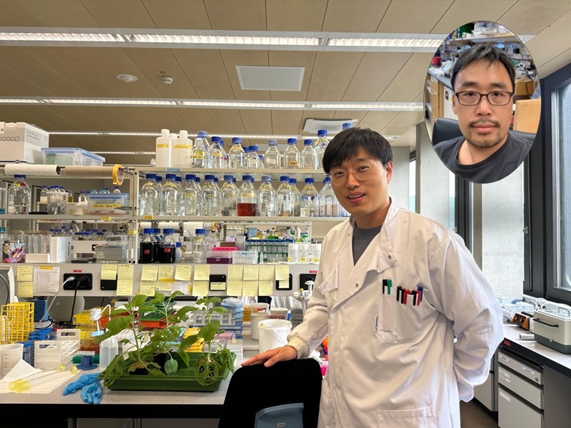 Why Do Plants Attack Themselves? The Secret of Genetic Conflict Revealed
<Professor Ji-Joon Song of the KAIST Department of Biological Sciences>
Plants, with their unique immune systems, sometimes launch 'autoimmune responses' by mistakenly identifying their own protein structures as pathogens. In particular, 'hybrid necrosis,' a phenomenon where descendant plants fail to grow healthily and perish after cross-breeding different varieties, has long been a difficult challenge for botanists and agricultural researchers. In response, an international research team has successfully elucidated the mechanism inducing plant autoimmune responses and proposed a novel strategy for cultivar improvement that can predict and avoid these reactions.
Professor Ji-Joon Song's research team at KAIST, in collaboration with teams from the National University of Singapore (NUS) and the University of Oxford, announced on the 21st of July that they have elucidated the structure and function of the 'DM3' protein complex, which triggers plant autoimmune responses, using cryo-electron microscopy (Cryo-EM) technology.
This research is drawing attention because it identifies defects in protein structure as the cause of hybrid necrosis, which occurs due to an abnormal reaction of immune receptors during cross-breeding between plant hybrids.
This protein (DM3) is originally an enzyme involved in the plant's immune response, but problems arise when the structure of the DM3 protein is damaged in a specific protein combination called 'DANGEROUS MIX (DM)'.
Notably, one variant of DM3, the 'DM3Col-0' variant, forms a stable complex with six proteins and is recognized as normal, thus not triggering an immune response. In contrast, another 'DM3Hh-0' variant has improper binding between its six proteins, causing the plant to recognize it as an 'abnormal state' and trigger an immune alarm, leading to autoimmunity.
The research team visualized this structure using atomic-resolution cryo-electron microscopy (Cryo-EM) and revealed that the immune-inducing ability is not due to the enzymatic function of the DM3 protein, but rather to 'differences in protein binding affinity.'
<Figure 1. Mechanism of Plant Autoimmunity Triggered by the Collapse of the DM3 Protein Complex>
This demonstrates that plants can initiate an immune response by recognizing not only 'external pathogens' but also 'internal protein structures' when they undergo abnormal changes, treating them as if they were pathogens.
The study shows how sensitively the plant immune system changes and triggers autoimmune responses when genes are mixed and protein structures change during the cross-breeding of different plant varieties. It significantly advanced the understanding of genetic incompatibility that can occur during natural cross-breeding and cultivar improvement processes.
Dr. Gijeong Kim, the co-first author, stated, "Through international research collaboration, we presented a new perspective on understanding the plant immune system by leveraging the autoimmune phenomenon, completing a high-quality study that encompasses structural biochemistry, genetics, and cell biological experiments."
Professor Ji-Joon Song of the KAIST Department of Biological Sciences, who led the research, said, "The fact that the immune system can detect not only external pathogens but also structural abnormalities in its own proteins will set a new standard for plant biotechnology and crop breeding strategies. Cryo-electron microscopy-based structural analysis will be an important tool for understanding the essence of gene interactions."
This research, with Professor Ji-Joon Song and Professor Eunyoung Chae of the University of Oxford as co-corresponding authors, Dr. Gijeong Kim (currently a postdoctoral researcher at the University of Zurich) and Dr. Wei-Lin Wan of the National University of Singapore as co-first authors, and Ph.D candidate Nayun Kim, as the second author, was published on July 17th in Molecular Cell, a sister journal of the international academic journal Cell.
This research was supported by the KAIST Grand Challenge 30 project.
Article Title: Structural determinants of DANGEROUS MIX 3, an alpha/beta hydrolase that triggers NLR-mediated genetic incompatibility in plants DOI: https://doi.org/10.1016/j.molcel.2025.06.021
2025.07.21 View 4207
Why Do Plants Attack Themselves? The Secret of Genetic Conflict Revealed
<Professor Ji-Joon Song of the KAIST Department of Biological Sciences>
Plants, with their unique immune systems, sometimes launch 'autoimmune responses' by mistakenly identifying their own protein structures as pathogens. In particular, 'hybrid necrosis,' a phenomenon where descendant plants fail to grow healthily and perish after cross-breeding different varieties, has long been a difficult challenge for botanists and agricultural researchers. In response, an international research team has successfully elucidated the mechanism inducing plant autoimmune responses and proposed a novel strategy for cultivar improvement that can predict and avoid these reactions.
Professor Ji-Joon Song's research team at KAIST, in collaboration with teams from the National University of Singapore (NUS) and the University of Oxford, announced on the 21st of July that they have elucidated the structure and function of the 'DM3' protein complex, which triggers plant autoimmune responses, using cryo-electron microscopy (Cryo-EM) technology.
This research is drawing attention because it identifies defects in protein structure as the cause of hybrid necrosis, which occurs due to an abnormal reaction of immune receptors during cross-breeding between plant hybrids.
This protein (DM3) is originally an enzyme involved in the plant's immune response, but problems arise when the structure of the DM3 protein is damaged in a specific protein combination called 'DANGEROUS MIX (DM)'.
Notably, one variant of DM3, the 'DM3Col-0' variant, forms a stable complex with six proteins and is recognized as normal, thus not triggering an immune response. In contrast, another 'DM3Hh-0' variant has improper binding between its six proteins, causing the plant to recognize it as an 'abnormal state' and trigger an immune alarm, leading to autoimmunity.
The research team visualized this structure using atomic-resolution cryo-electron microscopy (Cryo-EM) and revealed that the immune-inducing ability is not due to the enzymatic function of the DM3 protein, but rather to 'differences in protein binding affinity.'
<Figure 1. Mechanism of Plant Autoimmunity Triggered by the Collapse of the DM3 Protein Complex>
This demonstrates that plants can initiate an immune response by recognizing not only 'external pathogens' but also 'internal protein structures' when they undergo abnormal changes, treating them as if they were pathogens.
The study shows how sensitively the plant immune system changes and triggers autoimmune responses when genes are mixed and protein structures change during the cross-breeding of different plant varieties. It significantly advanced the understanding of genetic incompatibility that can occur during natural cross-breeding and cultivar improvement processes.
Dr. Gijeong Kim, the co-first author, stated, "Through international research collaboration, we presented a new perspective on understanding the plant immune system by leveraging the autoimmune phenomenon, completing a high-quality study that encompasses structural biochemistry, genetics, and cell biological experiments."
Professor Ji-Joon Song of the KAIST Department of Biological Sciences, who led the research, said, "The fact that the immune system can detect not only external pathogens but also structural abnormalities in its own proteins will set a new standard for plant biotechnology and crop breeding strategies. Cryo-electron microscopy-based structural analysis will be an important tool for understanding the essence of gene interactions."
This research, with Professor Ji-Joon Song and Professor Eunyoung Chae of the University of Oxford as co-corresponding authors, Dr. Gijeong Kim (currently a postdoctoral researcher at the University of Zurich) and Dr. Wei-Lin Wan of the National University of Singapore as co-first authors, and Ph.D candidate Nayun Kim, as the second author, was published on July 17th in Molecular Cell, a sister journal of the international academic journal Cell.
This research was supported by the KAIST Grand Challenge 30 project.
Article Title: Structural determinants of DANGEROUS MIX 3, an alpha/beta hydrolase that triggers NLR-mediated genetic incompatibility in plants DOI: https://doi.org/10.1016/j.molcel.2025.06.021
2025.07.21 View 4207 -
 KAIST Ushers in Era of Predicting ‘Optimal Alloys’ Using AI, Without High-Temperature Experiments
<Picture1.(From Left) Prof. Seungbum Hong, Ph.D candidate Youngwoo Choi>
Steel alloys used in automobiles and machinery parts are typically manufactured through a melting process at high temperatures. The phenomenon where the components remain unchanged during melting is called “congruent melting.” KAIST researchers have now addressed this process—traditionally only possible through high-temperature experiments—using artificial intelligence (AI). This study draws attention as it proposes a new direction for future alloy development by predicting in advance how well alloy components will mix during melting, a long-standing challenge in the field.
KAIST (President Kwang Hyung Lee) announced on the 14th of July that Professor Seungbum Hong’s research team from the Department of Materials Science and Engineering, in international collaboration with Professor Chris Wolverton’s group at Northwestern University, has developed a high-accuracy machine learning model that predicts whether alloy components will remain stable during melting. This was achieved using formation energy data derived from Density Functional Theory (DFT)* calculations.
*Density Functional Theory (DFT): A computational quantum mechanical method used to investigate the electronic structure of many-body systems, especially atoms, molecules, and solids, based on electron density.
The research team combined formation energy values obtained via DFT with experimental melting reaction data to train a machine learning model on 4,536 binary compounds.
Among the various machine learning algorithms tested, the XGBoost-based classification model demonstrated the highest accuracy in predicting whether alloys would mix well, achieving a prediction accuracy of approximately 82.5%. The team also applied the Shapley value method* to analyze the key features of the model. One major finding was that sharp changes in the slope of the formation energy curve (referred to as “convex hull sharpness”) were the most significant factor. A steep slope indicates a composition with energetically favorable (i.e., stable) formation.
*Shapley value: An explainability method in AI used to determine how much each feature contributed to a prediction.
The most notable significance of this study is that it predicts alloy melting behavior without performing high-temperature experiments. This is especially useful for materials such as high-entropy alloys or ultra-heat-resistant alloys, which are difficult to handle experimentally. The approach could also be extended to the design of complex multi-component alloy systems in the future.
Furthermore, the physical indicators identified by the AI model showed high consistency with actual experimental results on how well alloys mix and remain stable. This suggests that the model could be broadly applied to the development of various metal materials and the prediction of structural stability.
Professor Seungbum Hong of KAIST stated, “This research demonstrates how data-driven predictive materials development is possible by integrating computational methods, experimental data, and machine learning—departing from the traditional experience-based alloy design.” He added, “In the future, by incorporating state-of-the-art AI techniques such as generative models and reinforcement learning, we could enter an era where completely new alloys are designed automatically.”
<Model performance and feature importance analysis for predicting melting congruency. (a) SHAP summary plot showing the impact of individual features on model predictions. (b) Confusion matrix illustrating the model’s classification performance. (c) Receiver operating characteristic (ROC) curve with an AUC (area under the curve) score of 0.87, indicating a strong classification performance.>
Ph.D. candidate Youngwoo Choi, from the Department of Materials Science and Engineering at KAIST, participated as the first author. The study was published in the May issue of APL Machine Learning, a prestigious journal in the field of machine learning published by the American Institute of Physics, and was selected as a “Featured Article.”
※ Paper title: Machine learning-based melting congruency prediction of binary compounds using density functional theory-calculated formation energy ※ DOI: 10.1063/5.0247514
This research was supported by the Ministry of Science and ICT and the National Research Foundation of Korea.
2025.07.14 View 3756
KAIST Ushers in Era of Predicting ‘Optimal Alloys’ Using AI, Without High-Temperature Experiments
<Picture1.(From Left) Prof. Seungbum Hong, Ph.D candidate Youngwoo Choi>
Steel alloys used in automobiles and machinery parts are typically manufactured through a melting process at high temperatures. The phenomenon where the components remain unchanged during melting is called “congruent melting.” KAIST researchers have now addressed this process—traditionally only possible through high-temperature experiments—using artificial intelligence (AI). This study draws attention as it proposes a new direction for future alloy development by predicting in advance how well alloy components will mix during melting, a long-standing challenge in the field.
KAIST (President Kwang Hyung Lee) announced on the 14th of July that Professor Seungbum Hong’s research team from the Department of Materials Science and Engineering, in international collaboration with Professor Chris Wolverton’s group at Northwestern University, has developed a high-accuracy machine learning model that predicts whether alloy components will remain stable during melting. This was achieved using formation energy data derived from Density Functional Theory (DFT)* calculations.
*Density Functional Theory (DFT): A computational quantum mechanical method used to investigate the electronic structure of many-body systems, especially atoms, molecules, and solids, based on electron density.
The research team combined formation energy values obtained via DFT with experimental melting reaction data to train a machine learning model on 4,536 binary compounds.
Among the various machine learning algorithms tested, the XGBoost-based classification model demonstrated the highest accuracy in predicting whether alloys would mix well, achieving a prediction accuracy of approximately 82.5%. The team also applied the Shapley value method* to analyze the key features of the model. One major finding was that sharp changes in the slope of the formation energy curve (referred to as “convex hull sharpness”) were the most significant factor. A steep slope indicates a composition with energetically favorable (i.e., stable) formation.
*Shapley value: An explainability method in AI used to determine how much each feature contributed to a prediction.
The most notable significance of this study is that it predicts alloy melting behavior without performing high-temperature experiments. This is especially useful for materials such as high-entropy alloys or ultra-heat-resistant alloys, which are difficult to handle experimentally. The approach could also be extended to the design of complex multi-component alloy systems in the future.
Furthermore, the physical indicators identified by the AI model showed high consistency with actual experimental results on how well alloys mix and remain stable. This suggests that the model could be broadly applied to the development of various metal materials and the prediction of structural stability.
Professor Seungbum Hong of KAIST stated, “This research demonstrates how data-driven predictive materials development is possible by integrating computational methods, experimental data, and machine learning—departing from the traditional experience-based alloy design.” He added, “In the future, by incorporating state-of-the-art AI techniques such as generative models and reinforcement learning, we could enter an era where completely new alloys are designed automatically.”
<Model performance and feature importance analysis for predicting melting congruency. (a) SHAP summary plot showing the impact of individual features on model predictions. (b) Confusion matrix illustrating the model’s classification performance. (c) Receiver operating characteristic (ROC) curve with an AUC (area under the curve) score of 0.87, indicating a strong classification performance.>
Ph.D. candidate Youngwoo Choi, from the Department of Materials Science and Engineering at KAIST, participated as the first author. The study was published in the May issue of APL Machine Learning, a prestigious journal in the field of machine learning published by the American Institute of Physics, and was selected as a “Featured Article.”
※ Paper title: Machine learning-based melting congruency prediction of binary compounds using density functional theory-calculated formation energy ※ DOI: 10.1063/5.0247514
This research was supported by the Ministry of Science and ICT and the National Research Foundation of Korea.
2025.07.14 View 3756 -
 KAIST Turns an Unprecedented Idea into Reality: Quantum Computing with Magnets
What started as an idea under KAIST’s Global Singularity Research Project—"Can we build a quantum computer using magnets?"—has now become a scientific reality. A KAIST-led international research team has successfully demonstrated a core quantum computing technology using magnetic materials (ferromagnets) for the first time in the world.
KAIST (represented by President Kwang-Hyung Lee) announced on the 6th of May that a team led by Professor Kab-Jin Kim from the Department of Physics, in collaboration with the Argonne National Laboratory and the University of Illinois Urbana-Champaign (UIUC), has developed a “photon-magnon hybrid chip” and successfully implemented real-time, multi-pulse interference using magnetic materials—marking a global first.
< Photo 1. Dr. Moojune Song (left) and Professor Kab-Jin Kim (right) of KAIST Department of Physics >
In simple terms, the researchers developed a special chip that synchronizes light and internal magnetic vibrations (magnons), enabling the transmission of phase information between distant magnets. They succeeded in observing and controlling interference between multiple signals in real time. This marks the first experimental evidence that magnets can serve as key components in quantum computing, serving as a pivotal step toward magnet-based quantum platforms.
The N and S poles of a magnet stem from the spin of electrons inside atoms. When many atoms align, their collective spin vibrations create a quantum particle known as a “magnon.”
Magnons are especially promising because of their nonreciprocal nature—they can carry information in only one direction, which makes them suitable for quantum noise isolation in compact quantum chips. They can also couple with both light and microwaves, enabling the potential for long-distance quantum communication over tens of kilometers.
Moreover, using special materials like antiferromagnets could allow quantum computers to operate at terahertz (THz) frequencies, far surpassing today’s hardware limitations, and possibly enabling room-temperature quantum computing without the need for bulky cryogenic equipment.
To build such a system, however, one must be able to transmit, measure, and control the phase information of magnons—the starting point and propagation of their waveforms—in real time. This had not been achieved until now.
< Figure 1. Superconducting Circuit-Based Magnon-Photon Hybrid System. (a) Schematic diagram of the device. A NbN superconducting resonator circuit fabricated on a silicon substrate is coupled with spherical YIG magnets (250 μm diameter), and magnons are generated and measured in real-time via a vertical antenna. (b) Photograph of the actual device. The distance between the two YIG spheres is 12 mm, a distance at which they cannot influence each other without the superconducting circuit. >
Professor Kim’s team used two tiny magnetic spheres made of Yttrium Iron Garnet (YIG) placed 12 mm apart with a superconducting resonator in between—similar to those used in quantum processors by Google and IBM. They input pulses into one magnet and successfully observed lossless transmission of magnon vibrations to the second magnet via the superconducting circuit.
They confirmed that from single nanosecond pulses to four microwave pulses, the magnon vibrations maintained their phase information and demonstrated predictable constructive or destructive interference in real time—known as coherent interference.
By adjusting the pulse frequencies and their intervals, the researchers could also freely control the interference patterns of magnons, effectively showing for the first time that electrical signals can be used to manipulate magnonic quantum states.
This work demonstrated that quantum gate operations using multiple pulses—a fundamental technique in quantum information processing—can be implemented using a hybrid system of magnetic materials and superconducting circuits. This opens the door for the practical use of magnet-based quantum devices.
< Figure 2. Experimental Data. (a) Measurement results of magnon-magnon band anticrossing via continuous wave measurement, showing the formation of a strong coupling hybrid system. (b) Magnon pulse exchange oscillation phenomenon between YIG spheres upon single pulse application. It can be seen that magnon information is coherently transmitted at regular time intervals through the superconducting circuit. (c,d) Magnon interference phenomenon upon dual pulse application. The magnon information state can be arbitrarily controlled by adjusting the time interval and carrier frequency between pulses. >
Professor Kab-Jin Kim stated, “This project began with a bold, even unconventional idea proposed to the Global Singularity Research Program: ‘What if we could build a quantum computer with magnets?’ The journey has been fascinating, and this study not only opens a new field of quantum spintronics, but also marks a turning point in developing high-efficiency quantum information processing devices.”
The research was co-led by postdoctoral researcher Moojune Song (KAIST), Dr. Yi Li and Dr. Valentine Novosad from Argonne National Lab, and Prof. Axel Hoffmann’s team at UIUC. The results were published in Nature Communications on April 17 and npj Spintronics on April 1, 2025.
Paper 1: Single-shot magnon interference in a magnon-superconducting-resonator hybrid circuit, Nat. Commun. 16, 3649 (2025)
DOI: https://doi.org/10.1038/s41467-025-58482-2
Paper 2: Single-shot electrical detection of short-wavelength magnon pulse transmission in a magnonic ultra-thin-film waveguide, npj Spintronics 3, 12 (2025)
DOI: https://doi.org/10.1038/s44306-025-00072-5
The research was supported by KAIST’s Global Singularity Research Initiative, the National Research Foundation of Korea (including the Mid-Career Researcher, Leading Research Center, and Quantum Information Science Human Resource Development programs), and the U.S. Department of Energy.
2025.06.12 View 11861
KAIST Turns an Unprecedented Idea into Reality: Quantum Computing with Magnets
What started as an idea under KAIST’s Global Singularity Research Project—"Can we build a quantum computer using magnets?"—has now become a scientific reality. A KAIST-led international research team has successfully demonstrated a core quantum computing technology using magnetic materials (ferromagnets) for the first time in the world.
KAIST (represented by President Kwang-Hyung Lee) announced on the 6th of May that a team led by Professor Kab-Jin Kim from the Department of Physics, in collaboration with the Argonne National Laboratory and the University of Illinois Urbana-Champaign (UIUC), has developed a “photon-magnon hybrid chip” and successfully implemented real-time, multi-pulse interference using magnetic materials—marking a global first.
< Photo 1. Dr. Moojune Song (left) and Professor Kab-Jin Kim (right) of KAIST Department of Physics >
In simple terms, the researchers developed a special chip that synchronizes light and internal magnetic vibrations (magnons), enabling the transmission of phase information between distant magnets. They succeeded in observing and controlling interference between multiple signals in real time. This marks the first experimental evidence that magnets can serve as key components in quantum computing, serving as a pivotal step toward magnet-based quantum platforms.
The N and S poles of a magnet stem from the spin of electrons inside atoms. When many atoms align, their collective spin vibrations create a quantum particle known as a “magnon.”
Magnons are especially promising because of their nonreciprocal nature—they can carry information in only one direction, which makes them suitable for quantum noise isolation in compact quantum chips. They can also couple with both light and microwaves, enabling the potential for long-distance quantum communication over tens of kilometers.
Moreover, using special materials like antiferromagnets could allow quantum computers to operate at terahertz (THz) frequencies, far surpassing today’s hardware limitations, and possibly enabling room-temperature quantum computing without the need for bulky cryogenic equipment.
To build such a system, however, one must be able to transmit, measure, and control the phase information of magnons—the starting point and propagation of their waveforms—in real time. This had not been achieved until now.
< Figure 1. Superconducting Circuit-Based Magnon-Photon Hybrid System. (a) Schematic diagram of the device. A NbN superconducting resonator circuit fabricated on a silicon substrate is coupled with spherical YIG magnets (250 μm diameter), and magnons are generated and measured in real-time via a vertical antenna. (b) Photograph of the actual device. The distance between the two YIG spheres is 12 mm, a distance at which they cannot influence each other without the superconducting circuit. >
Professor Kim’s team used two tiny magnetic spheres made of Yttrium Iron Garnet (YIG) placed 12 mm apart with a superconducting resonator in between—similar to those used in quantum processors by Google and IBM. They input pulses into one magnet and successfully observed lossless transmission of magnon vibrations to the second magnet via the superconducting circuit.
They confirmed that from single nanosecond pulses to four microwave pulses, the magnon vibrations maintained their phase information and demonstrated predictable constructive or destructive interference in real time—known as coherent interference.
By adjusting the pulse frequencies and their intervals, the researchers could also freely control the interference patterns of magnons, effectively showing for the first time that electrical signals can be used to manipulate magnonic quantum states.
This work demonstrated that quantum gate operations using multiple pulses—a fundamental technique in quantum information processing—can be implemented using a hybrid system of magnetic materials and superconducting circuits. This opens the door for the practical use of magnet-based quantum devices.
< Figure 2. Experimental Data. (a) Measurement results of magnon-magnon band anticrossing via continuous wave measurement, showing the formation of a strong coupling hybrid system. (b) Magnon pulse exchange oscillation phenomenon between YIG spheres upon single pulse application. It can be seen that magnon information is coherently transmitted at regular time intervals through the superconducting circuit. (c,d) Magnon interference phenomenon upon dual pulse application. The magnon information state can be arbitrarily controlled by adjusting the time interval and carrier frequency between pulses. >
Professor Kab-Jin Kim stated, “This project began with a bold, even unconventional idea proposed to the Global Singularity Research Program: ‘What if we could build a quantum computer with magnets?’ The journey has been fascinating, and this study not only opens a new field of quantum spintronics, but also marks a turning point in developing high-efficiency quantum information processing devices.”
The research was co-led by postdoctoral researcher Moojune Song (KAIST), Dr. Yi Li and Dr. Valentine Novosad from Argonne National Lab, and Prof. Axel Hoffmann’s team at UIUC. The results were published in Nature Communications on April 17 and npj Spintronics on April 1, 2025.
Paper 1: Single-shot magnon interference in a magnon-superconducting-resonator hybrid circuit, Nat. Commun. 16, 3649 (2025)
DOI: https://doi.org/10.1038/s41467-025-58482-2
Paper 2: Single-shot electrical detection of short-wavelength magnon pulse transmission in a magnonic ultra-thin-film waveguide, npj Spintronics 3, 12 (2025)
DOI: https://doi.org/10.1038/s44306-025-00072-5
The research was supported by KAIST’s Global Singularity Research Initiative, the National Research Foundation of Korea (including the Mid-Career Researcher, Leading Research Center, and Quantum Information Science Human Resource Development programs), and the U.S. Department of Energy.
2025.06.12 View 11861