Atom
-
 Energy Storage Using Oxygen to Boost Battery Performance
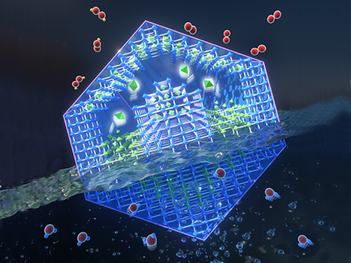
Researchers have presented a novel electrode material for advanced energy storage device that is directly charged with oxygen from the air. Professor Jeung Ku Kang’s team synthesized and preserved the sub-nanometric particles of atomic cluster sizes at high mass loadings within metal-organic frameworks (MOF) by controlling the behavior of reactants at the molecular level. This new strategy ensures high performance for lithium-oxygen batteries, acclaimed as a next-generation energy storage technology and widely used in electric vehicles.
Lithium-oxygen batteries in principle can generate ten times higher energy densities than conventional lithium-ion batteries, but they suffer from very poor cyclability. One of the methods to improve cycle stability is to reduce the overpotential of electrocatalysts in cathode electrodes. When the size of an electrocatalyst material is reduced to the atomic level, the increased surface energy leads to increased activity while significantly accelerating the material’s agglomeration.
As a solution to this challenge, Professor Kang from the Department of Materials Science and Engineering aimed to maintain the improved activity by stabilizing atomic-scale sized electrocatalysts into the sub-nanometric spaces. This is a novel strategy for simultaneously producing and stabilizing atomic-level electrocatalysts within metal-organic frameworks (MOFs).
Metal-organic frameworks continuously assemble metal ions and organic linkers.
The team controlled hydrogen affinities between water molecules to separate them and transfer the isolated water molecules one by one through the sub-nanometric pores of MOFs. The transferred water molecules reacted with cobalt ions to form di-nuclear cobalt hydroxide under precisely controlled synthetic conditions, then the atomic-level cobalt hydroxide is stabilized inside the sub-nanometric pores.
The di-nuclear cobalt hydroxide that is stabilized in the sub-nanometric pores of metal-organic frameworks (MOFs) reduced the overpotential by 63.9% and showed ten-fold improvements in the life cycle.
Professor Kang said, “Simultaneously generating and stabilizing atomic-level electrocatalysts within MOFs can diversify materials according to numerous combinations of metal and organic linkers. It can expand not only the development of electrocatalysts, but also various research fields such as photocatalysts, medicine, the environment, and petrochemicals.”
This study was reported in Advanced Science (Title: Autogenous Production and Stabilization of Highly Loaded Sub-Nanometric Particles within Multishell Hollow Metal-Organic Frameworks and Their Utilization for High Performance in Li-O2 Batteries).
This research was mainly supported by the Global Frontier R&D Program of the Ministry of Science, ICT & Planning (Grant No. 2013M3A6B1078884) funded by the Ministry of Science, ICT & Future Planning, and the National Research Foundation of Korea (Grant No. 2019M3E6A1104196).
Profile:Professor Jeung Ku Kang
jeungku@kaist.ac.kr
http://nanosf.kaist.ac.kr/
Nano Materials Simulation and Fabrication Laboratory
Department of Materials Science and Engineering
KAIST
2020.06.15 View 15070
Energy Storage Using Oxygen to Boost Battery Performance
Researchers have presented a novel electrode material for advanced energy storage device that is directly charged with oxygen from the air. Professor Jeung Ku Kang’s team synthesized and preserved the sub-nanometric particles of atomic cluster sizes at high mass loadings within metal-organic frameworks (MOF) by controlling the behavior of reactants at the molecular level. This new strategy ensures high performance for lithium-oxygen batteries, acclaimed as a next-generation energy storage technology and widely used in electric vehicles.
Lithium-oxygen batteries in principle can generate ten times higher energy densities than conventional lithium-ion batteries, but they suffer from very poor cyclability. One of the methods to improve cycle stability is to reduce the overpotential of electrocatalysts in cathode electrodes. When the size of an electrocatalyst material is reduced to the atomic level, the increased surface energy leads to increased activity while significantly accelerating the material’s agglomeration.
As a solution to this challenge, Professor Kang from the Department of Materials Science and Engineering aimed to maintain the improved activity by stabilizing atomic-scale sized electrocatalysts into the sub-nanometric spaces. This is a novel strategy for simultaneously producing and stabilizing atomic-level electrocatalysts within metal-organic frameworks (MOFs).
Metal-organic frameworks continuously assemble metal ions and organic linkers.
The team controlled hydrogen affinities between water molecules to separate them and transfer the isolated water molecules one by one through the sub-nanometric pores of MOFs. The transferred water molecules reacted with cobalt ions to form di-nuclear cobalt hydroxide under precisely controlled synthetic conditions, then the atomic-level cobalt hydroxide is stabilized inside the sub-nanometric pores.
The di-nuclear cobalt hydroxide that is stabilized in the sub-nanometric pores of metal-organic frameworks (MOFs) reduced the overpotential by 63.9% and showed ten-fold improvements in the life cycle.
Professor Kang said, “Simultaneously generating and stabilizing atomic-level electrocatalysts within MOFs can diversify materials according to numerous combinations of metal and organic linkers. It can expand not only the development of electrocatalysts, but also various research fields such as photocatalysts, medicine, the environment, and petrochemicals.”
This study was reported in Advanced Science (Title: Autogenous Production and Stabilization of Highly Loaded Sub-Nanometric Particles within Multishell Hollow Metal-Organic Frameworks and Their Utilization for High Performance in Li-O2 Batteries).
This research was mainly supported by the Global Frontier R&D Program of the Ministry of Science, ICT & Planning (Grant No. 2013M3A6B1078884) funded by the Ministry of Science, ICT & Future Planning, and the National Research Foundation of Korea (Grant No. 2019M3E6A1104196).
Profile:Professor Jeung Ku Kang
jeungku@kaist.ac.kr
http://nanosf.kaist.ac.kr/
Nano Materials Simulation and Fabrication Laboratory
Department of Materials Science and Engineering
KAIST
2020.06.15 View 15070 -
 From Dark to Light in a Flash: Smart Film Lets Windows Switch Autonomously
Researchers have developed a new easy-to-use smart optical film technology that allows smart window devices to autonomously switch between transparent and opaque states in response to the surrounding light conditions.
The proposed 3D hybrid nanocomposite film with a highly periodic network structure has empirically demonstrated its high speed and performance, enabling the smart window to quantify and self-regulate its high-contrast optical transmittance. As a proof of concept, a mobile-app-enabled smart window device for Internet of Things (IoT) applications has been realized using the proposed smart optical film with successful expansion to the 3-by-3-inch scale. This energy-efficient and cost-effective technology holds great promise for future use in various applications that require active optical transmission modulation.
Flexible optical transmission modulation technologies for smart applications including privacy-protection windows, zero-energy buildings, and beam projection screens have been in the spotlight in recent years. Conventional technologies that used external stimuli such as electricity, heat, or light to modulate optical transmission had only limited applications due to their slow response speeds, unnecessary color switching, and low durability, stability, and safety.
The optical transmission modulation contrast achieved by controlling the light scattering interfaces on non-periodic 2D surface structures that often have low optical density such as cracks, wrinkles, and pillars is also generally low. In addition, since the light scattering interfaces are exposed and not subject to any passivation, they can be vulnerable to external damage and may lose optical transmission modulation functions. Furthermore, in-plane scattering interfaces that randomly exist on the surface make large-area modulation with uniformity difficult.
Inspired by these limitations, a KAIST research team led by Professor Seokwoo Jeon from the Department of Materials Science and Engineering and Professor Jung-Wuk Hong of the Civil and Environmental Engineering Department used proximity-field nanopatterning (PnP) technology that effectively produces highly periodic 3D hybrid nanostructures, and an atomic layer deposition (ALD) technique that allows the precise control of oxide deposition and the high-quality fabrication of semiconductor devices.
The team then successfully produced a large-scale smart optical film with a size of 3 by 3 inches in which ultrathin alumina nanoshells are inserted between the elastomers in a periodic 3D nanonetwork.
This “mechano-responsive” 3D hybrid nanocomposite film with a highly periodic network structure is the largest smart optical transmission modulation film that exists. The film has been shown to have state-of-the-art optical transmission modulation of up to 74% at visible wavelengths from 90% initial transmission to 16% in the scattering state under strain. Its durability and stability were proved by more than 10,000 tests of harsh mechanical deformation including stretching, releasing, bending, and being placed under high temperatures of up to 70°C. When this film was used, the transmittance of the smart window device was adjusted promptly and automatically within one second in response to the surrounding light conditions. Through these experiments, the underlying physics of optical scattering phenomena occurring in the heterogeneous interfaces were identified. Their findings were reported in the online edition of Advanced Science on April 26. KAIST Professor Jong-Hwa Shin’s group and Professor Young-Seok Shim at Silla University also collaborated on this project.
Donghwi Cho, a PhD candidate in materials science and engineering at KAIST and co-lead author of the study, said, “Our smart optical film technology can better control high-contrast optical transmittance by relatively simple operating principles and with low energy consumption and costs.”
“When this technology is applied by simply attaching the film to a conventional smart window glass surface without replacing the existing window system, fast switching and uniform tinting are possible while also securing durability, stability, and safety. In addition, its wide range of applications for stretchable or rollable devices such as wall-type displays for a beam projection screen will also fulfill aesthetic needs,” he added.
This work was supported by the National Research Foundation of Korea (NRF), and the Korean Ministries of Science, ICT and Future Planning (MSIP), and Science and ICT (MSIT).
Publication:
Cho, D, et al. (2020) ‘High-Contrast Optical Modulation from Strain-Indicated Nanogaps at 3D Heterogeneous Interfaces’ Advanced Science, 1903708. Available online at https://doi.org/10.1002/advs.201903708
Profile: Seokwoo Jeon, PhD
Professor
jeon39@kaist.ac.kr
https://fdml.kaist.ac.kr/
Flexible Device and Metamaterials Lab (FDML)
Department of Materials Science and Engineering (MSE)
Korea Advanced Institute of Science and Technology (KAIST)
https://www.kaist.ac.krDaejeon 34141, Korea
Profile: Jung-Wuk Hong, PhD
Associate Professor
j.hong@kaist.ac.kr
http://aaml.kaist.ac.kr
Advanced Applied Mechanics Laboratory (AAML)
Department of Civil and Environmental Engineering
KAIST
Profile: Donghwi Cho
PhD Candidate
roy0202@kaist.ac.krFDML, MSE, KAIST
Profile: Young-Seok Shim, PhD
Assistant Professor
ysshim@silla.ac.kr
Division of Materials Science and Engineering Silla University
https://www.silla.ac.kr
Busan 46958, Korea
(END)
2020.06.02 View 15826
From Dark to Light in a Flash: Smart Film Lets Windows Switch Autonomously
Researchers have developed a new easy-to-use smart optical film technology that allows smart window devices to autonomously switch between transparent and opaque states in response to the surrounding light conditions.
The proposed 3D hybrid nanocomposite film with a highly periodic network structure has empirically demonstrated its high speed and performance, enabling the smart window to quantify and self-regulate its high-contrast optical transmittance. As a proof of concept, a mobile-app-enabled smart window device for Internet of Things (IoT) applications has been realized using the proposed smart optical film with successful expansion to the 3-by-3-inch scale. This energy-efficient and cost-effective technology holds great promise for future use in various applications that require active optical transmission modulation.
Flexible optical transmission modulation technologies for smart applications including privacy-protection windows, zero-energy buildings, and beam projection screens have been in the spotlight in recent years. Conventional technologies that used external stimuli such as electricity, heat, or light to modulate optical transmission had only limited applications due to their slow response speeds, unnecessary color switching, and low durability, stability, and safety.
The optical transmission modulation contrast achieved by controlling the light scattering interfaces on non-periodic 2D surface structures that often have low optical density such as cracks, wrinkles, and pillars is also generally low. In addition, since the light scattering interfaces are exposed and not subject to any passivation, they can be vulnerable to external damage and may lose optical transmission modulation functions. Furthermore, in-plane scattering interfaces that randomly exist on the surface make large-area modulation with uniformity difficult.
Inspired by these limitations, a KAIST research team led by Professor Seokwoo Jeon from the Department of Materials Science and Engineering and Professor Jung-Wuk Hong of the Civil and Environmental Engineering Department used proximity-field nanopatterning (PnP) technology that effectively produces highly periodic 3D hybrid nanostructures, and an atomic layer deposition (ALD) technique that allows the precise control of oxide deposition and the high-quality fabrication of semiconductor devices.
The team then successfully produced a large-scale smart optical film with a size of 3 by 3 inches in which ultrathin alumina nanoshells are inserted between the elastomers in a periodic 3D nanonetwork.
This “mechano-responsive” 3D hybrid nanocomposite film with a highly periodic network structure is the largest smart optical transmission modulation film that exists. The film has been shown to have state-of-the-art optical transmission modulation of up to 74% at visible wavelengths from 90% initial transmission to 16% in the scattering state under strain. Its durability and stability were proved by more than 10,000 tests of harsh mechanical deformation including stretching, releasing, bending, and being placed under high temperatures of up to 70°C. When this film was used, the transmittance of the smart window device was adjusted promptly and automatically within one second in response to the surrounding light conditions. Through these experiments, the underlying physics of optical scattering phenomena occurring in the heterogeneous interfaces were identified. Their findings were reported in the online edition of Advanced Science on April 26. KAIST Professor Jong-Hwa Shin’s group and Professor Young-Seok Shim at Silla University also collaborated on this project.
Donghwi Cho, a PhD candidate in materials science and engineering at KAIST and co-lead author of the study, said, “Our smart optical film technology can better control high-contrast optical transmittance by relatively simple operating principles and with low energy consumption and costs.”
“When this technology is applied by simply attaching the film to a conventional smart window glass surface without replacing the existing window system, fast switching and uniform tinting are possible while also securing durability, stability, and safety. In addition, its wide range of applications for stretchable or rollable devices such as wall-type displays for a beam projection screen will also fulfill aesthetic needs,” he added.
This work was supported by the National Research Foundation of Korea (NRF), and the Korean Ministries of Science, ICT and Future Planning (MSIP), and Science and ICT (MSIT).
Publication:
Cho, D, et al. (2020) ‘High-Contrast Optical Modulation from Strain-Indicated Nanogaps at 3D Heterogeneous Interfaces’ Advanced Science, 1903708. Available online at https://doi.org/10.1002/advs.201903708
Profile: Seokwoo Jeon, PhD
Professor
jeon39@kaist.ac.kr
https://fdml.kaist.ac.kr/
Flexible Device and Metamaterials Lab (FDML)
Department of Materials Science and Engineering (MSE)
Korea Advanced Institute of Science and Technology (KAIST)
https://www.kaist.ac.krDaejeon 34141, Korea
Profile: Jung-Wuk Hong, PhD
Associate Professor
j.hong@kaist.ac.kr
http://aaml.kaist.ac.kr
Advanced Applied Mechanics Laboratory (AAML)
Department of Civil and Environmental Engineering
KAIST
Profile: Donghwi Cho
PhD Candidate
roy0202@kaist.ac.krFDML, MSE, KAIST
Profile: Young-Seok Shim, PhD
Assistant Professor
ysshim@silla.ac.kr
Division of Materials Science and Engineering Silla University
https://www.silla.ac.kr
Busan 46958, Korea
(END)
2020.06.02 View 15826 -
 Visualization of Functional Components to Characterize Optimal Composite Electrodes
Researchers have developed a visualization method that will determine the distribution of components in battery electrodes using atomic force microscopy. The method provides insights into the optimal conditions of composite electrodes and takes us one step closer to being able to manufacture next-generation all-solid-state batteries.
Lithium-ion batteries are widely used in smart devices and vehicles. However, their flammability makes them a safety concern, arising from potential leakage of liquid electrolytes.
All-solid-state lithium ion batteries have emerged as an alternative because of their better safety and wider electrochemical stability. Despite their advantages, all-solid-state lithium ion batteries still have drawbacks such as limited ion conductivity, insufficient contact areas, and high interfacial resistance between the electrode and solid electrolyte.
To solve these issues, studies have been conducted on composite electrodes in which lithium ion conducting additives are dispersed as a medium to provide ion conductive paths at the interface and increase the overall ionic conductivity.
It is very important to identify the shape and distribution of the components used in active materials, ion conductors, binders, and conductive additives on a microscopic scale for significantly improving the battery operation performance.
The developed method is able to distinguish regions of each component based on detected signal sensitivity, by using various modes of atomic force microscopy on a multiscale basis, including electrochemical strain microscopy and lateral force microscopy.
For this research project, both conventional electrodes and composite electrodes were tested, and the results were compared. Individual regions were distinguished and nanoscale correlation between ion reactivity distribution and friction force distribution within a single region was determined to examine the effect of the distribution of binder on the electrochemical strain.
The research team explored the electrochemical strain microscopy amplitude/phase and lateral force microscopy friction force dependence on the AC drive voltage and the tip loading force, and used their sensitivities as markers for each component in the composite anode.
This method allows for direct multiscale observation of the composite electrode in ambient condition, distinguishing various components and measuring their properties simultaneously.
Lead author Dr. Hongjun Kim said, “It is easy to prepare the test sample for observation while providing much higher spatial resolution and intensity resolution for detected signals.” He added, “The method also has the advantage of providing 3D surface morphology information for the observed specimens.”
Professor Seungbum Hong from the Department of Material Sciences and Engineering said, “This analytical technique using atomic force microscopy will be useful for quantitatively understanding what role each component of a composite material plays in the final properties.”
“Our method not only will suggest the new direction for next-generation all-solid-state battery design on a multiscale basis but also lay the groundwork for innovation in the manufacturing process of other electrochemical materials.”
This study is published in ACS Applied Energy Materials and supported by the Big Science Research and Development Project under the Ministry of Science and ICT and the National Research Foundation of Korea, the Basic Research Project under the Wearable Platform Materials Technology Center, and KAIST Global Singularity Research Program for 2019 and 2020.
Publication:Kim, H, et al. (2020) ‘Visualization of Functional Components in a Lithium Silicon Titanium Phosphate-Natural Graphite Composite Anode’. ACS Applied Energy Materials, Volume 3, Issue 4, pp. 3253-3261. Available online at https://doi.org/10.1021/acsaem.9b02045
Profile:
Seungbum Hong
Professor
seungbum@kaist.ac.kr
http://mii.kaist.ac.kr/
Materials Imaging and Integration Laboratory
Department of Material Sciences and Engineering
KAIST
2020.05.22 View 11985
Visualization of Functional Components to Characterize Optimal Composite Electrodes
Researchers have developed a visualization method that will determine the distribution of components in battery electrodes using atomic force microscopy. The method provides insights into the optimal conditions of composite electrodes and takes us one step closer to being able to manufacture next-generation all-solid-state batteries.
Lithium-ion batteries are widely used in smart devices and vehicles. However, their flammability makes them a safety concern, arising from potential leakage of liquid electrolytes.
All-solid-state lithium ion batteries have emerged as an alternative because of their better safety and wider electrochemical stability. Despite their advantages, all-solid-state lithium ion batteries still have drawbacks such as limited ion conductivity, insufficient contact areas, and high interfacial resistance between the electrode and solid electrolyte.
To solve these issues, studies have been conducted on composite electrodes in which lithium ion conducting additives are dispersed as a medium to provide ion conductive paths at the interface and increase the overall ionic conductivity.
It is very important to identify the shape and distribution of the components used in active materials, ion conductors, binders, and conductive additives on a microscopic scale for significantly improving the battery operation performance.
The developed method is able to distinguish regions of each component based on detected signal sensitivity, by using various modes of atomic force microscopy on a multiscale basis, including electrochemical strain microscopy and lateral force microscopy.
For this research project, both conventional electrodes and composite electrodes were tested, and the results were compared. Individual regions were distinguished and nanoscale correlation between ion reactivity distribution and friction force distribution within a single region was determined to examine the effect of the distribution of binder on the electrochemical strain.
The research team explored the electrochemical strain microscopy amplitude/phase and lateral force microscopy friction force dependence on the AC drive voltage and the tip loading force, and used their sensitivities as markers for each component in the composite anode.
This method allows for direct multiscale observation of the composite electrode in ambient condition, distinguishing various components and measuring their properties simultaneously.
Lead author Dr. Hongjun Kim said, “It is easy to prepare the test sample for observation while providing much higher spatial resolution and intensity resolution for detected signals.” He added, “The method also has the advantage of providing 3D surface morphology information for the observed specimens.”
Professor Seungbum Hong from the Department of Material Sciences and Engineering said, “This analytical technique using atomic force microscopy will be useful for quantitatively understanding what role each component of a composite material plays in the final properties.”
“Our method not only will suggest the new direction for next-generation all-solid-state battery design on a multiscale basis but also lay the groundwork for innovation in the manufacturing process of other electrochemical materials.”
This study is published in ACS Applied Energy Materials and supported by the Big Science Research and Development Project under the Ministry of Science and ICT and the National Research Foundation of Korea, the Basic Research Project under the Wearable Platform Materials Technology Center, and KAIST Global Singularity Research Program for 2019 and 2020.
Publication:Kim, H, et al. (2020) ‘Visualization of Functional Components in a Lithium Silicon Titanium Phosphate-Natural Graphite Composite Anode’. ACS Applied Energy Materials, Volume 3, Issue 4, pp. 3253-3261. Available online at https://doi.org/10.1021/acsaem.9b02045
Profile:
Seungbum Hong
Professor
seungbum@kaist.ac.kr
http://mii.kaist.ac.kr/
Materials Imaging and Integration Laboratory
Department of Material Sciences and Engineering
KAIST
2020.05.22 View 11985 -
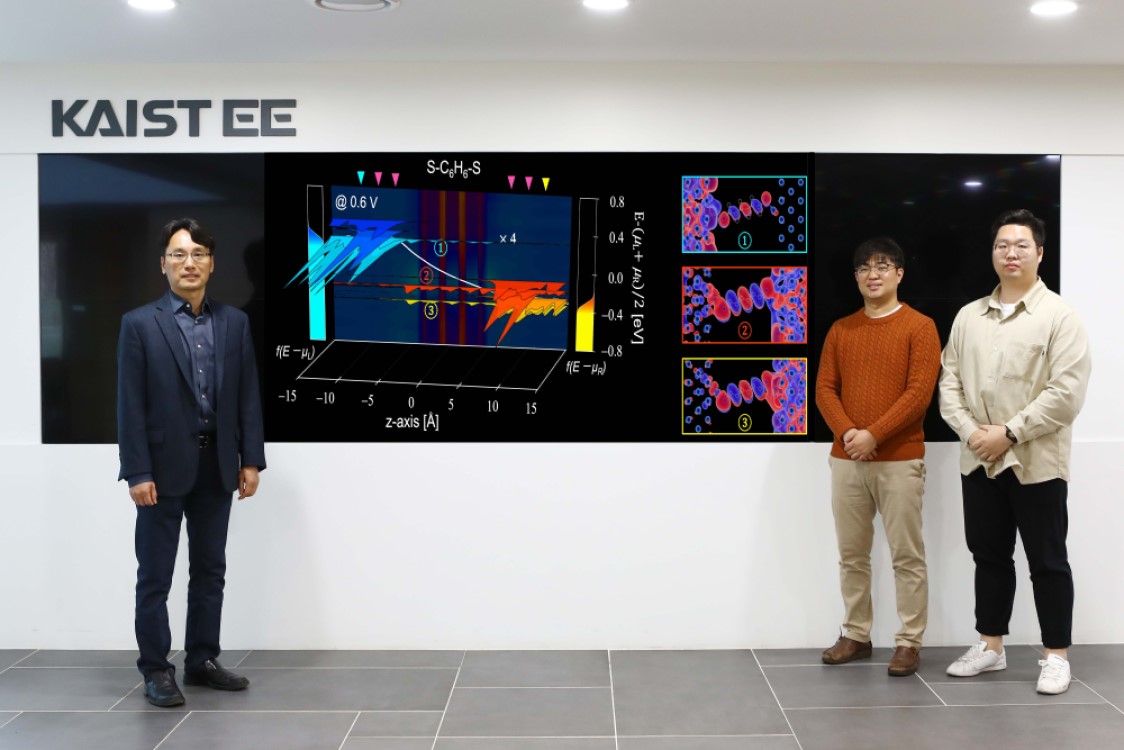 A Theoretical Boost to Nano-Scale Devices
- Researchers calculate the quasi-Fermi levels in molecular junctions applying an initio approach. -
Semiconductor companies are struggling to develop devices that are mere nanometers in size, and much of the challenge lies in being able to more accurately describe the underlying physics at that nano-scale. But a new computational approach that has been in the works for a decade could break down these barriers.
Devices using semiconductors, from computers to solar cells, have enjoyed tremendous efficiency improvements in the last few decades. Famously, one of the co-founders of Intel, Gordon Moore, observed that the number of transistors in an integrated circuit doubles about every two years—and this ‘Moore’s law’ held true for some time.
In recent years, however, such gains have slowed as firms that attempt to engineer nano-scale transistors hit the limits of miniaturization at the atomic level.
Researchers with the School of Electrical Engineering at KAIST have developed a new approach to the underlying physics of semiconductors.
“With open quantum systems as the main research target of our lab, we were revisiting concepts that had been taken for granted and even appear in standard semiconductor physics textbooks such as the voltage drop in operating semiconductor devices,” said the lead researcher Professor Yong-Hoon Kim. “Questioning how all these concepts could be understood and possibly revised at the nano-scale, it was clear that there was something incomplete about our current understanding.”
“And as the semiconductor chips are being scaled down to the atomic level, coming up with a better theory to describe semiconductor devices has become an urgent task.”
The current understanding states that semiconductors are materials that act like half-way houses between conductors, like copper or steel, and insulators, like rubber or Styrofoam. They sometimes conduct electricity, but not always. This makes them a great material for intentionally controlling the flow of current, which in turn is useful for constructing the simple on/off switches—transistors—that are the foundation of memory and logic devices in computers.
In order to ‘switch on’ a semiconductor, a current or light source is applied, exciting an electron in an atom to jump from what is called a ‘valence band,’ which is filled with electrons, up to the ‘conduction band,’ which is originally unfilled or only partially filled with electrons. Electrons that have jumped up to the conduction band thanks to external stimuli and the remaining ‘holes’ are now able to move about and act as charge carriers to flow electric current.
The physical concept that describes the populations of the electrons in the conduction band and the holes in the valence band and the energy required to make this jump is formulated in terms of the so-called ‘Fermi level.’ For example, you need to know the Fermi levels of the electrons and holes in order to know what amount of energy you are going to get out of a solar cell, including losses.
But the Fermi level concept is only straightforwardly defined so long as a semiconductor device is at equilibrium—sitting on a shelf doing nothing—and the whole point of semiconductor devices is not to leave them on the shelf.
Some 70 years ago, William Shockley, the Nobel Prize-winning co-inventor of the transistor at the Bell Labs, came up with a bit of a theoretical fudge, the ‘quasi-Fermi level,’ or QFL, enabling rough prediction and measurement of the interaction between valence band holes and conduction band electrons, and this has worked pretty well until now.
“But when you are working at the scale of just a few nanometers, the methods to theoretically calculate or experimentally measure the splitting of QFLs were just not available,” said Professor Kim.
This means that at this scale, issues such as errors relating to voltage drop take on much greater significance.
Kim’s team worked for nearly ten years on developing a novel theoretical description of nano-scale quantum electron transport that can replace the standard method—and the software that allows them to put it to use. This involved the further development of a bit of math known as the Density Functional Theory that simplifies the equations describing the interactions of electrons, and which has been very useful in other fields such as high-throughput computational materials discovery.
For the first time, they were able to calculate the QFL splitting, offering a new understanding of the relationship between voltage drop and quantum electron transport in atomic scale devices.
In addition to looking into various interesting non-equilibrium quantum phenomena with their novel methodology, the team is now further developing their software into a computer-aided design tool to be used by semiconductor companies for developing and fabricating advanced semiconductor devices.
The study, featured at the Proceedings of the National Academy of Sciences of the USA on May 12, was supported by the National Research Foundation and the Korea Institute of Science and Technology Information Supercomputing Center.
Image caption: The newly developed formalism and QFL splitting analysis led to new ways of characterizing extremely scaled-down semiconductor devices and the technology computer-aided design (TCAD) of next- generation nano-electronic/energy/bio devices.
Image credit: Yong-Hoon Kim, KAIST
Image usage restrictions: News organizations may use or redistribute this image, with proper attribution, as part of news coverage of this paper only.
Publication:
Juho Lee, Hyeonwoo Yeo, and Yong-Hoon Kim. (2020) ‘Quasi-Fermi level splitting in nanoscale junctions from ab initio.’ Proceedings of the National Academy of Sciences of the United States of America (PNAS), Volume 117, Issue 19, pp.10142-101488. Available online at https://doi.org/10.1073/pnas.1921273117
Profile:
Yong-Hoon Kim
Professor
y.h.kim@kaist.ac.kr
http://nanocore.kaist.ac.kr/
1st-Principles Nano-Device Computing Lab
School of Electrical Engineering
KAIST
(END)
2020.05.15 View 10217
A Theoretical Boost to Nano-Scale Devices
- Researchers calculate the quasi-Fermi levels in molecular junctions applying an initio approach. -
Semiconductor companies are struggling to develop devices that are mere nanometers in size, and much of the challenge lies in being able to more accurately describe the underlying physics at that nano-scale. But a new computational approach that has been in the works for a decade could break down these barriers.
Devices using semiconductors, from computers to solar cells, have enjoyed tremendous efficiency improvements in the last few decades. Famously, one of the co-founders of Intel, Gordon Moore, observed that the number of transistors in an integrated circuit doubles about every two years—and this ‘Moore’s law’ held true for some time.
In recent years, however, such gains have slowed as firms that attempt to engineer nano-scale transistors hit the limits of miniaturization at the atomic level.
Researchers with the School of Electrical Engineering at KAIST have developed a new approach to the underlying physics of semiconductors.
“With open quantum systems as the main research target of our lab, we were revisiting concepts that had been taken for granted and even appear in standard semiconductor physics textbooks such as the voltage drop in operating semiconductor devices,” said the lead researcher Professor Yong-Hoon Kim. “Questioning how all these concepts could be understood and possibly revised at the nano-scale, it was clear that there was something incomplete about our current understanding.”
“And as the semiconductor chips are being scaled down to the atomic level, coming up with a better theory to describe semiconductor devices has become an urgent task.”
The current understanding states that semiconductors are materials that act like half-way houses between conductors, like copper or steel, and insulators, like rubber or Styrofoam. They sometimes conduct electricity, but not always. This makes them a great material for intentionally controlling the flow of current, which in turn is useful for constructing the simple on/off switches—transistors—that are the foundation of memory and logic devices in computers.
In order to ‘switch on’ a semiconductor, a current or light source is applied, exciting an electron in an atom to jump from what is called a ‘valence band,’ which is filled with electrons, up to the ‘conduction band,’ which is originally unfilled or only partially filled with electrons. Electrons that have jumped up to the conduction band thanks to external stimuli and the remaining ‘holes’ are now able to move about and act as charge carriers to flow electric current.
The physical concept that describes the populations of the electrons in the conduction band and the holes in the valence band and the energy required to make this jump is formulated in terms of the so-called ‘Fermi level.’ For example, you need to know the Fermi levels of the electrons and holes in order to know what amount of energy you are going to get out of a solar cell, including losses.
But the Fermi level concept is only straightforwardly defined so long as a semiconductor device is at equilibrium—sitting on a shelf doing nothing—and the whole point of semiconductor devices is not to leave them on the shelf.
Some 70 years ago, William Shockley, the Nobel Prize-winning co-inventor of the transistor at the Bell Labs, came up with a bit of a theoretical fudge, the ‘quasi-Fermi level,’ or QFL, enabling rough prediction and measurement of the interaction between valence band holes and conduction band electrons, and this has worked pretty well until now.
“But when you are working at the scale of just a few nanometers, the methods to theoretically calculate or experimentally measure the splitting of QFLs were just not available,” said Professor Kim.
This means that at this scale, issues such as errors relating to voltage drop take on much greater significance.
Kim’s team worked for nearly ten years on developing a novel theoretical description of nano-scale quantum electron transport that can replace the standard method—and the software that allows them to put it to use. This involved the further development of a bit of math known as the Density Functional Theory that simplifies the equations describing the interactions of electrons, and which has been very useful in other fields such as high-throughput computational materials discovery.
For the first time, they were able to calculate the QFL splitting, offering a new understanding of the relationship between voltage drop and quantum electron transport in atomic scale devices.
In addition to looking into various interesting non-equilibrium quantum phenomena with their novel methodology, the team is now further developing their software into a computer-aided design tool to be used by semiconductor companies for developing and fabricating advanced semiconductor devices.
The study, featured at the Proceedings of the National Academy of Sciences of the USA on May 12, was supported by the National Research Foundation and the Korea Institute of Science and Technology Information Supercomputing Center.
Image caption: The newly developed formalism and QFL splitting analysis led to new ways of characterizing extremely scaled-down semiconductor devices and the technology computer-aided design (TCAD) of next- generation nano-electronic/energy/bio devices.
Image credit: Yong-Hoon Kim, KAIST
Image usage restrictions: News organizations may use or redistribute this image, with proper attribution, as part of news coverage of this paper only.
Publication:
Juho Lee, Hyeonwoo Yeo, and Yong-Hoon Kim. (2020) ‘Quasi-Fermi level splitting in nanoscale junctions from ab initio.’ Proceedings of the National Academy of Sciences of the United States of America (PNAS), Volume 117, Issue 19, pp.10142-101488. Available online at https://doi.org/10.1073/pnas.1921273117
Profile:
Yong-Hoon Kim
Professor
y.h.kim@kaist.ac.kr
http://nanocore.kaist.ac.kr/
1st-Principles Nano-Device Computing Lab
School of Electrical Engineering
KAIST
(END)
2020.05.15 View 10217 -
 Highly Efficient and Stable Double Layer Solar Cell Developed
Solar cells convert light into energy, but they can be inefficient and vulnerable to the environment, degrading with, ironically, too much light or other factors, including moisture and low temperature. An international research team has developed a new type of solar cell that can both withstand environmental hazards and is 26.7% efficient in power conversion.
They published their results on March 26 in Science.
The researchers, led by Byungha Shin, a professor from the Department of Materials Science and Engineering at KAIST, focused on developing a new class of light-absorbing material, called a wide bandgap perovskite. The material has a highly effective crystal structure that can process the power needs, but it can become problematic when exposed to environmental hazards, such as moisture. Researchers have made some progress increasing the efficiency of solar cells based on perovskite, but the material has greater potential than what was previously achieved.
To achieve better performance, Shin and his team built a double layer solar cell, called tandem, in which two or more light absorbers are stacked together to better utilize solar energy. To use perovskite in these tandem devices, the scientists modified the material’s optical property, which allows it to absorb a wider range of solar energy. Without the adjustment, the material is not as useful in achieving high performing tandem solar cells. The modification of the optical property of perovskite, however, comes with a penalty — the material becomes hugely vulnerable to the environment, in particular, to light.
To counteract the wide bandgap perovskite’s delicate nature, the researchers engineered combinations of molecules composing a two-dimensional layer in the perovskite, stabilizing the solar cells.
“We developed a high-quality wide bandgap perovskite material and, in combination with silicon solar cells, achieved world-class perovskite-silicon tandem cells,” Shin said.
The development was only possible due to the engineering method, in which the mixing ratio of the molecules building the two-dimensional layer are carefully controlled. In this case, the perovskite material not only improved efficiency of the resulting solar cell but also gained durability, retaining 80% of its initial power conversion capability even after 1,000 hours of continuous illumination. This is the first time such a high efficiency has been achieved with a wide bandgap perovskite single layer alone, according to Shin.
“Such high-efficiency wide bandgap perovskite is an essential technology for achieving ultra-high efficiency of perovskite-silicon tandem (double layer) solar cells,” Shin said. “The results also show the importance of bandgap matching of upper and lower cells in these tandem solar cells.”
The researchers, having stabilized the wide bandgap perovskite material, are now focused on developing even more efficient tandem solar cells that are expected to have more than 30% of power conversion efficiency, something that no one has achieved yet,
“Our ultimate goal is to develop ultra-high-efficiency tandem solar cells that contribute to the increase of shared solar energy among all energy sources,” Shin said. “We want to contribute to making the planet healthier.”
This work was supported by the National Research Foundation of Korea, the Korea Institute of Energy Technology Evaluation and Planning, the Ministry of Trade Industry and Energy of Korea, and the U.S. Department of Energy.
Other contributors include Daehan Kim, Jekyung Kim, Passarut Boonmongkolras, Seong Ryul Pae and Minkyu Kim, all of whom affiliated with the Department of Materials Science and Engineering at KAIST. Other authors include Byron W. Larson, Sean P. Dunfield, Chuanxiao Xiao, Jinhui Tong, Fei Zhang, Joseph J. Berry, Kai Zhu and Dong Hoe Kim, all of who are affiliated with the National Renewable Energy Laboratory in Colorado. Dunfield is also affiliated with the Materials Science and Engineering Program at the University of Colorado; Berry is also affiliated with the Department of Physics and the Renewable and Sustainable Energy Institute at the University of Colorado Boulder; and Kim is also affiliated with the Department of Nanotechnology and Advanced Materials Engineering at Sejong University. Hee Joon Jung and Vinayak Dravid of the Department of Materials Science and Engineering at Northwestern University; Ik Jae Park, Su Geun Ji and Jin Young Kim of the Department of Materials Science and Engineering at Seoul National University; and Seok Beom Kang of the Department of Nanotechnology and Advanced Materials Engineering of Sejong University also contributed.
Image credit: Professor Byungha Shin, KAIST
Image usage restrictions: News organizations may use or redistribute this image, with proper attribution, as part of news coverage of this paper only.
Publication: Kim et al. (2020) “Efficient, stable silicon tandem cells enabled by anion-engineered wide band gap perovskites”. Science. Available online at https://doi.org/10.1126/science.aba3433
Profile:
Byungha Shin
Professor
byungha@kaist.ac.kr
http://energymatlab.kaist.ac.kr/
Department of Materials Science and Engineering
KAIST
Profile:
Daehan Kim
Ph.D. Candidate
zxzx4592@kaist.ac.kr
http://energymatlab.kaist.ac.kr/
Department of Materials Science and Engineering
KAIST
(END)
2020.03.27 View 24624
Highly Efficient and Stable Double Layer Solar Cell Developed
Solar cells convert light into energy, but they can be inefficient and vulnerable to the environment, degrading with, ironically, too much light or other factors, including moisture and low temperature. An international research team has developed a new type of solar cell that can both withstand environmental hazards and is 26.7% efficient in power conversion.
They published their results on March 26 in Science.
The researchers, led by Byungha Shin, a professor from the Department of Materials Science and Engineering at KAIST, focused on developing a new class of light-absorbing material, called a wide bandgap perovskite. The material has a highly effective crystal structure that can process the power needs, but it can become problematic when exposed to environmental hazards, such as moisture. Researchers have made some progress increasing the efficiency of solar cells based on perovskite, but the material has greater potential than what was previously achieved.
To achieve better performance, Shin and his team built a double layer solar cell, called tandem, in which two or more light absorbers are stacked together to better utilize solar energy. To use perovskite in these tandem devices, the scientists modified the material’s optical property, which allows it to absorb a wider range of solar energy. Without the adjustment, the material is not as useful in achieving high performing tandem solar cells. The modification of the optical property of perovskite, however, comes with a penalty — the material becomes hugely vulnerable to the environment, in particular, to light.
To counteract the wide bandgap perovskite’s delicate nature, the researchers engineered combinations of molecules composing a two-dimensional layer in the perovskite, stabilizing the solar cells.
“We developed a high-quality wide bandgap perovskite material and, in combination with silicon solar cells, achieved world-class perovskite-silicon tandem cells,” Shin said.
The development was only possible due to the engineering method, in which the mixing ratio of the molecules building the two-dimensional layer are carefully controlled. In this case, the perovskite material not only improved efficiency of the resulting solar cell but also gained durability, retaining 80% of its initial power conversion capability even after 1,000 hours of continuous illumination. This is the first time such a high efficiency has been achieved with a wide bandgap perovskite single layer alone, according to Shin.
“Such high-efficiency wide bandgap perovskite is an essential technology for achieving ultra-high efficiency of perovskite-silicon tandem (double layer) solar cells,” Shin said. “The results also show the importance of bandgap matching of upper and lower cells in these tandem solar cells.”
The researchers, having stabilized the wide bandgap perovskite material, are now focused on developing even more efficient tandem solar cells that are expected to have more than 30% of power conversion efficiency, something that no one has achieved yet,
“Our ultimate goal is to develop ultra-high-efficiency tandem solar cells that contribute to the increase of shared solar energy among all energy sources,” Shin said. “We want to contribute to making the planet healthier.”
This work was supported by the National Research Foundation of Korea, the Korea Institute of Energy Technology Evaluation and Planning, the Ministry of Trade Industry and Energy of Korea, and the U.S. Department of Energy.
Other contributors include Daehan Kim, Jekyung Kim, Passarut Boonmongkolras, Seong Ryul Pae and Minkyu Kim, all of whom affiliated with the Department of Materials Science and Engineering at KAIST. Other authors include Byron W. Larson, Sean P. Dunfield, Chuanxiao Xiao, Jinhui Tong, Fei Zhang, Joseph J. Berry, Kai Zhu and Dong Hoe Kim, all of who are affiliated with the National Renewable Energy Laboratory in Colorado. Dunfield is also affiliated with the Materials Science and Engineering Program at the University of Colorado; Berry is also affiliated with the Department of Physics and the Renewable and Sustainable Energy Institute at the University of Colorado Boulder; and Kim is also affiliated with the Department of Nanotechnology and Advanced Materials Engineering at Sejong University. Hee Joon Jung and Vinayak Dravid of the Department of Materials Science and Engineering at Northwestern University; Ik Jae Park, Su Geun Ji and Jin Young Kim of the Department of Materials Science and Engineering at Seoul National University; and Seok Beom Kang of the Department of Nanotechnology and Advanced Materials Engineering of Sejong University also contributed.
Image credit: Professor Byungha Shin, KAIST
Image usage restrictions: News organizations may use or redistribute this image, with proper attribution, as part of news coverage of this paper only.
Publication: Kim et al. (2020) “Efficient, stable silicon tandem cells enabled by anion-engineered wide band gap perovskites”. Science. Available online at https://doi.org/10.1126/science.aba3433
Profile:
Byungha Shin
Professor
byungha@kaist.ac.kr
http://energymatlab.kaist.ac.kr/
Department of Materials Science and Engineering
KAIST
Profile:
Daehan Kim
Ph.D. Candidate
zxzx4592@kaist.ac.kr
http://energymatlab.kaist.ac.kr/
Department of Materials Science and Engineering
KAIST
(END)
2020.03.27 View 24624 -
 Scientists Observe the Elusive Kondo Screening Cloud
Scientists ended a 50-year quest by directly observing a quantum phenomenon
An international research group of Professor Heung-Sun Sim has ended a 50-year quest by directly observing a quantum phenomenon known as a Kondo screening cloud. This research, published in Nature on March 11, opens a novel way to engineer spin screening and entanglement. According to the research, the cloud can mediate interactions between distant spins confined in quantum dots, which is a necessary protocol for semiconductor spin-based quantum information processing. This spin-spin interaction mediated by the Kondo cloud is unique since both its strength and sign (two spins favor either parallel or anti-parallel configuration) are electrically tunable, while conventional schemes cannot reverse the sign.
This phenomenon, which is important for many physical phenomena such as dilute magnetic impurities and spin glasses, is essentially a cloud that masks magnetic impurities in a material. It was known to exist but its spatial extension had never been observed, creating controversy over whether such an extension actually existed.
Magnetism arises from a property of electrons known as spin, meaning that they have angular momentum aligned in one of either two directions, conventionally known as up and down. However, due to a phenomenon known as the Kondo effect, the spins of conduction electrons—the electrons that flow freely in a material—become entangled with a localized magnetic impurity, and effectively screen it. The strength of this spin coupling, calibrated as a temperature, is known as the Kondo temperature.
The size of the cloud is another important parameter for a material containing multiple magnetic impurities because the spins in the cloud couple with one another and mediate the coupling between magnetic impurities when the clouds overlap. This happens in various materials such as Kondo lattices, spin glasses, and high temperature superconductors.
Although the Kondo effect for a single magnetic impurity is now a text-book subject in many-body physics, detection of its key object, the Kondo cloud and its length, has remained elusive despite many attempts during the past five decades. Experiments using nuclear magnetic resonance or scanning tunneling microscopy, two common methods for understanding the structure of matter, have either shown no signature of the cloud, or demonstrated a signature only at a very short distance, less than 1 nanometer, so much shorter than the predicted cloud size, which was in the micron range.
In the present study, the authors observed a Kondo screening cloud formed by an impurity defined as a localized electron spin in a quantum dot—a type of “artificial atom”—coupled to quasi-one-dimensional conduction electrons, and then used an interferometer to measure changes in the Kondo temperature, allowing them to investigate the presence of a cloud at the interferometer end.
Essentially, they slightly perturbed the conduction electrons at a location away from the quantum dot using an electrostatic gate. The wave of conducting electrons scattered by this perturbation returned back to the quantum dot and interfered with itself. This is similar to how a wave on a water surface being scattered by a wall forms a stripe pattern. The Kondo cloud is a quantum mechanical object which acts to preserve the wave nature of electrons inside the cloud.
Even though there is no direct electrostatic influence of the perturbation on the quantum dot, this interference modifies the Kondo signature measured by electron conductance through the quantum dot if the perturbation is present inside the cloud. In the study, the researchers found that the length as well as the shape of the cloud is universally scaled by the inverse of the Kondo temperature, and that the cloud’s size and shape were in good agreement with theoretical calculations.
Professor Sim at the Department of Physics proposed the method for detecting the Kondo cloud in the co-research with the RIKEN Center for Emergent Matter Science, the City University of Hong Kong, the University of Tokyo, and Ruhr University Bochum in Germany.
Professor Sim said, “The observed spin cloud is a micrometer-size object that has quantum mechanical wave nature and entanglement. This is why the spin cloud has not been observed despite a long search. It is remarkable in a fundamental and technical point of view that such a large quantum object can now be created, controlled, and detected.
Dr. Michihisa Yamamoto of the RIKEN Center for Emergent Matter Science also said, “It is very satisfying to have been able to obtain real space image of the Kondo cloud, as it is a real breakthrough for understanding various systems containing multiple magnetic impurities. The size of the Kondo cloud in semiconductors was found to be much larger than the typical size of semiconductor devices.”
Publication:
Borzenets et al. (2020) Observation of the Kondo screening cloud. Nature, 579. pp.210-213. Available online at https://doi.org/10.1038/s41586-020-2058-6
Profile:
Heung-Sun Sim, PhD
Professor
hssim@kaist.ac.kr
https://qet.kaist.ac.kr/
Quantum Electron Correlation & Transport Theory Group (QECT Lab)
https://qc.kaist.ac.kr/index.php/group1/
Center for Quantum Coherence In COndensed Matter
Department of Physics
https://www.kaist.ac.kr
Korea Advanced Institute of Science and Technology (KAIST)
Daejeon, Republic of Korea
2020.03.13 View 19178
Scientists Observe the Elusive Kondo Screening Cloud
Scientists ended a 50-year quest by directly observing a quantum phenomenon
An international research group of Professor Heung-Sun Sim has ended a 50-year quest by directly observing a quantum phenomenon known as a Kondo screening cloud. This research, published in Nature on March 11, opens a novel way to engineer spin screening and entanglement. According to the research, the cloud can mediate interactions between distant spins confined in quantum dots, which is a necessary protocol for semiconductor spin-based quantum information processing. This spin-spin interaction mediated by the Kondo cloud is unique since both its strength and sign (two spins favor either parallel or anti-parallel configuration) are electrically tunable, while conventional schemes cannot reverse the sign.
This phenomenon, which is important for many physical phenomena such as dilute magnetic impurities and spin glasses, is essentially a cloud that masks magnetic impurities in a material. It was known to exist but its spatial extension had never been observed, creating controversy over whether such an extension actually existed.
Magnetism arises from a property of electrons known as spin, meaning that they have angular momentum aligned in one of either two directions, conventionally known as up and down. However, due to a phenomenon known as the Kondo effect, the spins of conduction electrons—the electrons that flow freely in a material—become entangled with a localized magnetic impurity, and effectively screen it. The strength of this spin coupling, calibrated as a temperature, is known as the Kondo temperature.
The size of the cloud is another important parameter for a material containing multiple magnetic impurities because the spins in the cloud couple with one another and mediate the coupling between magnetic impurities when the clouds overlap. This happens in various materials such as Kondo lattices, spin glasses, and high temperature superconductors.
Although the Kondo effect for a single magnetic impurity is now a text-book subject in many-body physics, detection of its key object, the Kondo cloud and its length, has remained elusive despite many attempts during the past five decades. Experiments using nuclear magnetic resonance or scanning tunneling microscopy, two common methods for understanding the structure of matter, have either shown no signature of the cloud, or demonstrated a signature only at a very short distance, less than 1 nanometer, so much shorter than the predicted cloud size, which was in the micron range.
In the present study, the authors observed a Kondo screening cloud formed by an impurity defined as a localized electron spin in a quantum dot—a type of “artificial atom”—coupled to quasi-one-dimensional conduction electrons, and then used an interferometer to measure changes in the Kondo temperature, allowing them to investigate the presence of a cloud at the interferometer end.
Essentially, they slightly perturbed the conduction electrons at a location away from the quantum dot using an electrostatic gate. The wave of conducting electrons scattered by this perturbation returned back to the quantum dot and interfered with itself. This is similar to how a wave on a water surface being scattered by a wall forms a stripe pattern. The Kondo cloud is a quantum mechanical object which acts to preserve the wave nature of electrons inside the cloud.
Even though there is no direct electrostatic influence of the perturbation on the quantum dot, this interference modifies the Kondo signature measured by electron conductance through the quantum dot if the perturbation is present inside the cloud. In the study, the researchers found that the length as well as the shape of the cloud is universally scaled by the inverse of the Kondo temperature, and that the cloud’s size and shape were in good agreement with theoretical calculations.
Professor Sim at the Department of Physics proposed the method for detecting the Kondo cloud in the co-research with the RIKEN Center for Emergent Matter Science, the City University of Hong Kong, the University of Tokyo, and Ruhr University Bochum in Germany.
Professor Sim said, “The observed spin cloud is a micrometer-size object that has quantum mechanical wave nature and entanglement. This is why the spin cloud has not been observed despite a long search. It is remarkable in a fundamental and technical point of view that such a large quantum object can now be created, controlled, and detected.
Dr. Michihisa Yamamoto of the RIKEN Center for Emergent Matter Science also said, “It is very satisfying to have been able to obtain real space image of the Kondo cloud, as it is a real breakthrough for understanding various systems containing multiple magnetic impurities. The size of the Kondo cloud in semiconductors was found to be much larger than the typical size of semiconductor devices.”
Publication:
Borzenets et al. (2020) Observation of the Kondo screening cloud. Nature, 579. pp.210-213. Available online at https://doi.org/10.1038/s41586-020-2058-6
Profile:
Heung-Sun Sim, PhD
Professor
hssim@kaist.ac.kr
https://qet.kaist.ac.kr/
Quantum Electron Correlation & Transport Theory Group (QECT Lab)
https://qc.kaist.ac.kr/index.php/group1/
Center for Quantum Coherence In COndensed Matter
Department of Physics
https://www.kaist.ac.kr
Korea Advanced Institute of Science and Technology (KAIST)
Daejeon, Republic of Korea
2020.03.13 View 19178 -
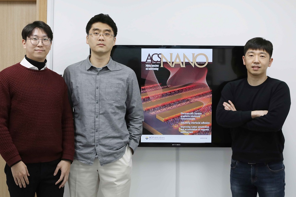 New Graphene-Based Metasurface Capable of Independent Amplitude and Phase Control of Light
Researchers described a new strategy of designing metamolecules that incorporates two independently controllable subwavelength meta-atoms. This two-parametric control of the metamolecule secures the complete control of both amplitude and the phase of light.
A KAIST research team in collaboration with the University of Wisconsin-Madison theoretically suggested a graphene-based active metasurface capable of independent amplitude and phase control of mid-infrared light. This research gives a new insight into modulating the mid-infrared wavefront with high resolution by solving the problem of the independent control of light amplitude and phase, which has remained a long-standing challenge.
Light modulation technology is essential for developing future optical devices such as holography, high-resolution imaging, and optical communication systems. Liquid crystals and a microelectromechanical system (MEMS) have previously been utilized to modulate light. However, both methods suffer from significantly limited driving speeds and unit pixel sizes larger than the diffraction limit, which consequently prevent their integration into photonic systems.
The metasurface platform is considered a strong candidate for the next generation of light modulation technology. Metasurfaces have optical properties that natural materials cannot have, and can overcome the limitations of conventional optical systems, such as forming a high-resolution image beyond the diffraction limit. In particular, the active metasurface is regarded as a technology with a wide range of applications due to its tunable optical characteristics with an electrical signal.
However, the previous active metasurfaces suffered from the inevitable correlation between light amplitude control and phase control. This problem is caused by the modulation mechanism of conventional metasurfaces. Conventional metasurfaces have been designed such that a metaatom only has one resonance condition, but a single resonant design inherently lacks the degrees of freedom to independently control the amplitude and phase of light.
The research team made a metaunit by combining two independently controllable metaatoms, dramatically improving the modulation range of active metasurfaces. The proposed metasurface can control the amplitude and phase of the mid-infrared light independently with a resolution beyond the diffraction limit, thus allowing complete control of the optical wavefront.
The research team theoretically confirmed the performance of the proposed active metasurface and the possibility of wavefront shaping using this design method. Furthermore, they developed an analytical method that can approximate the optical properties of metasurfaces without complex electromagnetic simulations. This analytical platform proposes a more intuitive and comprehensively applicable metasurface design guideline.
The proposed technology is expected to enable accurate wavefront shaping with a much higher spatial resolution than existing wavefront shaping technologies, which will be applied to active optical systems such as mid-infrared holography, high-speed beam steering devices that can be applied for LiDAR, and variable focus infrared lenses.
Professor Min Seok Jang commented, "This study showed the independent control amplitude and phase of light, which has been a long-standing quest in light modulator technology. The development of optical devices using complex wavefront control is expected to become more active in the future."
MS candidate Sangjun Han and Dr. Seyoon Kim of the University of Wisconsin-Madison are the co-first authors of the research, which was published and selected as the front cover of the January 28 edition of ACS Nano titled “Complete complex amplitude modulation with electronically tunable graphene plasmonic metamolecules.”
This research was funded by the Samsung Research Funding & Incubation Center for Future Technology.
Publication:
Han et al. (2020) Complete Complex Amplitude Modulation with Electronically Tunable Graphene Plasmonic Metamolecules. ACS Nano, Vol. 14, Issue 1, pp. 1166-1175. Available online at https://doi.org/10.1021/acsnano.9b09277
Profile: Prof. Min Seok Jang, MS, PhD
jang.minseok@kaist.ac.kr
http://jlab.kaist.ac.kr/
Associate Professor
Jang Research Group
School of Electrical Engineering
Korea Advanced Institute of Science and Technology (KAIST)
http://kaist.ac.kr
Daejeon, Republic of Korea
Profile: Sangjun Han
sangjun.han@kaist.ac.kr
MS Candidate
School of Electrical Engineering
Korea Advanced Institute of Science and Technology (KAIST)
http://kaist.ac.kr
Daejeon, Republic of Korea
(END)
2020.02.20 View 11163
New Graphene-Based Metasurface Capable of Independent Amplitude and Phase Control of Light
Researchers described a new strategy of designing metamolecules that incorporates two independently controllable subwavelength meta-atoms. This two-parametric control of the metamolecule secures the complete control of both amplitude and the phase of light.
A KAIST research team in collaboration with the University of Wisconsin-Madison theoretically suggested a graphene-based active metasurface capable of independent amplitude and phase control of mid-infrared light. This research gives a new insight into modulating the mid-infrared wavefront with high resolution by solving the problem of the independent control of light amplitude and phase, which has remained a long-standing challenge.
Light modulation technology is essential for developing future optical devices such as holography, high-resolution imaging, and optical communication systems. Liquid crystals and a microelectromechanical system (MEMS) have previously been utilized to modulate light. However, both methods suffer from significantly limited driving speeds and unit pixel sizes larger than the diffraction limit, which consequently prevent their integration into photonic systems.
The metasurface platform is considered a strong candidate for the next generation of light modulation technology. Metasurfaces have optical properties that natural materials cannot have, and can overcome the limitations of conventional optical systems, such as forming a high-resolution image beyond the diffraction limit. In particular, the active metasurface is regarded as a technology with a wide range of applications due to its tunable optical characteristics with an electrical signal.
However, the previous active metasurfaces suffered from the inevitable correlation between light amplitude control and phase control. This problem is caused by the modulation mechanism of conventional metasurfaces. Conventional metasurfaces have been designed such that a metaatom only has one resonance condition, but a single resonant design inherently lacks the degrees of freedom to independently control the amplitude and phase of light.
The research team made a metaunit by combining two independently controllable metaatoms, dramatically improving the modulation range of active metasurfaces. The proposed metasurface can control the amplitude and phase of the mid-infrared light independently with a resolution beyond the diffraction limit, thus allowing complete control of the optical wavefront.
The research team theoretically confirmed the performance of the proposed active metasurface and the possibility of wavefront shaping using this design method. Furthermore, they developed an analytical method that can approximate the optical properties of metasurfaces without complex electromagnetic simulations. This analytical platform proposes a more intuitive and comprehensively applicable metasurface design guideline.
The proposed technology is expected to enable accurate wavefront shaping with a much higher spatial resolution than existing wavefront shaping technologies, which will be applied to active optical systems such as mid-infrared holography, high-speed beam steering devices that can be applied for LiDAR, and variable focus infrared lenses.
Professor Min Seok Jang commented, "This study showed the independent control amplitude and phase of light, which has been a long-standing quest in light modulator technology. The development of optical devices using complex wavefront control is expected to become more active in the future."
MS candidate Sangjun Han and Dr. Seyoon Kim of the University of Wisconsin-Madison are the co-first authors of the research, which was published and selected as the front cover of the January 28 edition of ACS Nano titled “Complete complex amplitude modulation with electronically tunable graphene plasmonic metamolecules.”
This research was funded by the Samsung Research Funding & Incubation Center for Future Technology.
Publication:
Han et al. (2020) Complete Complex Amplitude Modulation with Electronically Tunable Graphene Plasmonic Metamolecules. ACS Nano, Vol. 14, Issue 1, pp. 1166-1175. Available online at https://doi.org/10.1021/acsnano.9b09277
Profile: Prof. Min Seok Jang, MS, PhD
jang.minseok@kaist.ac.kr
http://jlab.kaist.ac.kr/
Associate Professor
Jang Research Group
School of Electrical Engineering
Korea Advanced Institute of Science and Technology (KAIST)
http://kaist.ac.kr
Daejeon, Republic of Korea
Profile: Sangjun Han
sangjun.han@kaist.ac.kr
MS Candidate
School of Electrical Engineering
Korea Advanced Institute of Science and Technology (KAIST)
http://kaist.ac.kr
Daejeon, Republic of Korea
(END)
2020.02.20 View 11163 -
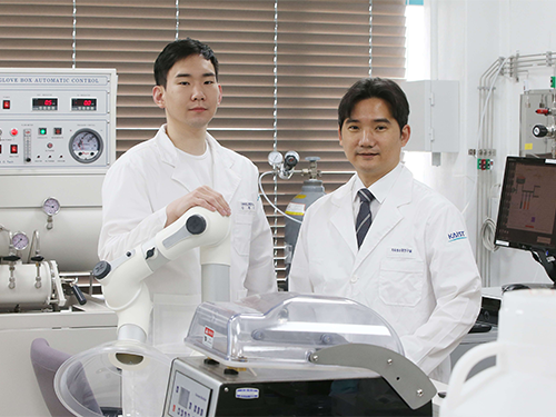
 Tungsten Suboxide Improves the Efficiency of Platinum in Hydrogen Production
< PhD Candidate Jinkyu Park and Professor Jinwoo Lee >
Researchers presented a new strategy for enhancing catalytic activity using tungsten suboxide as a single-atom catalyst (SAC). This strategy, which significantly improves hydrogen evolution reaction (HER) in metal platinum (pt) by 16.3 times, sheds light on the development of new electrochemical catalyst technologies.
Hydrogen has been touted as a promising alternative to fossil fuels. However, most of the conventional industrial hydrogen production methods come with environmental issues, releasing significant amounts of carbon dioxide and greenhouse gases.
Electrochemical water splitting is considered a potential approach for clean hydrogen production. Pt is one of the most commonly used catalysts to improve HER performance in electrochemical water splitting, but the high cost and scarcity of Pt remain key obstacles to mass commercial applications.
SACs, where all metal species are individually dispersed on a desired support material, have been identified as one way to reduce the amount of Pt usage, as they offer the maximum number of surface exposed Pt atoms.
Inspired by earlier studies, which mainly focused on SACs supported by carbon-based materials, a KAIST research team led by Professor Jinwoo Lee from the Department of Chemical and Biomolecular Engineering investigated the influence of support materials on the performance of SACs.
Professor Lee and his researchers suggested mesoporous tungsten suboxide as a new support material for atomically dispersed Pt, as this was expected to provide high electronic conductivity and have a synergetic effect with Pt.
They compared the performance of single-atom Pt supported by carbon and tungsten suboxide respectively. The results revealed that the support effect occurred with tungsten suboxide, in which the mass activity of a single-atom Pt supported by tungsten suboxide was 2.1 times greater than that of single-atom Pt supported by carbon, and 16.3 times higher than that of Pt nanoparticles supported by carbon.
The team indicated a change in the electronic structure of Pt via charge transfer from tungsten suboxide to Pt. This phenomenon was reported as a result of strong metal-support interaction between Pt and tungsten suboxide.
HER performance can be improved not only by changing the electronic structure of the supported metal, but also by inducing another support effect, the spillover effect, the research group reported. Hydrogen spillover is a phenomenon where adsorbed hydrogen migrates from one surface to another, and it occurs more easily as the Pt size becomes smaller.
The researchers compared the performance of single-atom Pt and Pt nanoparticles supported by tungsten suboxide. The single-atom Pt supported by tungsten suboxide exhibited a higher degree of hydrogen spillover phenomenon, which enhanced the Pt mass activity for hydrogen evolution up to 10.7 times compared to Pt nanoparticles supported by tungsten suboxide.
Professor Lee said, “Choosing the right support material is important for improving electrocatalysis in hydrogen production. The tungsten suboxide catalyst we used to support Pt in our study implies that interactions between the well-matched metal and support can drastically enhance the efficiency of the process.”
This research was supported by the Ministry of Science and ICT and introduced in the International Edition of the German journal Angewandte Chemie.
Figure. Schematic representation of hydrogen evolution reaction (HER) of pseudo single-atom Pt supported by tungsten suboxide
-Publication
Jinkyu Park, Dr. Seonggyu Lee, Hee-Eun Kim, Ara Cho, Seongbeen Kim, Dr. Youngjin Ye, Prof. Jeong Woo Han, Prof. Hyunjoo Lee, Dr. Jong Hyun Jang, and Prof. Jinwoo Lee. 2019. Investigation of the Support Effect in Atomically Dispersed Pt on WO3−x for Utilization of Pt in the Hydrogen Evolution Reaction. International Edition of Angewandte Chemie. Volume No. 58. Issue No. 45. 6 pages. https://doi.org/10.1002/anie.201908122
-ProfileProfessor Jinwoo LeeConvergence of Energy and Nano Science Laboratoryhttp://cens.kaist.ac.kr
Department of Chemical and Biomolecular EngineeringKAIST
2019.10.28 View 24202
Tungsten Suboxide Improves the Efficiency of Platinum in Hydrogen Production
< PhD Candidate Jinkyu Park and Professor Jinwoo Lee >
Researchers presented a new strategy for enhancing catalytic activity using tungsten suboxide as a single-atom catalyst (SAC). This strategy, which significantly improves hydrogen evolution reaction (HER) in metal platinum (pt) by 16.3 times, sheds light on the development of new electrochemical catalyst technologies.
Hydrogen has been touted as a promising alternative to fossil fuels. However, most of the conventional industrial hydrogen production methods come with environmental issues, releasing significant amounts of carbon dioxide and greenhouse gases.
Electrochemical water splitting is considered a potential approach for clean hydrogen production. Pt is one of the most commonly used catalysts to improve HER performance in electrochemical water splitting, but the high cost and scarcity of Pt remain key obstacles to mass commercial applications.
SACs, where all metal species are individually dispersed on a desired support material, have been identified as one way to reduce the amount of Pt usage, as they offer the maximum number of surface exposed Pt atoms.
Inspired by earlier studies, which mainly focused on SACs supported by carbon-based materials, a KAIST research team led by Professor Jinwoo Lee from the Department of Chemical and Biomolecular Engineering investigated the influence of support materials on the performance of SACs.
Professor Lee and his researchers suggested mesoporous tungsten suboxide as a new support material for atomically dispersed Pt, as this was expected to provide high electronic conductivity and have a synergetic effect with Pt.
They compared the performance of single-atom Pt supported by carbon and tungsten suboxide respectively. The results revealed that the support effect occurred with tungsten suboxide, in which the mass activity of a single-atom Pt supported by tungsten suboxide was 2.1 times greater than that of single-atom Pt supported by carbon, and 16.3 times higher than that of Pt nanoparticles supported by carbon.
The team indicated a change in the electronic structure of Pt via charge transfer from tungsten suboxide to Pt. This phenomenon was reported as a result of strong metal-support interaction between Pt and tungsten suboxide.
HER performance can be improved not only by changing the electronic structure of the supported metal, but also by inducing another support effect, the spillover effect, the research group reported. Hydrogen spillover is a phenomenon where adsorbed hydrogen migrates from one surface to another, and it occurs more easily as the Pt size becomes smaller.
The researchers compared the performance of single-atom Pt and Pt nanoparticles supported by tungsten suboxide. The single-atom Pt supported by tungsten suboxide exhibited a higher degree of hydrogen spillover phenomenon, which enhanced the Pt mass activity for hydrogen evolution up to 10.7 times compared to Pt nanoparticles supported by tungsten suboxide.
Professor Lee said, “Choosing the right support material is important for improving electrocatalysis in hydrogen production. The tungsten suboxide catalyst we used to support Pt in our study implies that interactions between the well-matched metal and support can drastically enhance the efficiency of the process.”
This research was supported by the Ministry of Science and ICT and introduced in the International Edition of the German journal Angewandte Chemie.
Figure. Schematic representation of hydrogen evolution reaction (HER) of pseudo single-atom Pt supported by tungsten suboxide
-Publication
Jinkyu Park, Dr. Seonggyu Lee, Hee-Eun Kim, Ara Cho, Seongbeen Kim, Dr. Youngjin Ye, Prof. Jeong Woo Han, Prof. Hyunjoo Lee, Dr. Jong Hyun Jang, and Prof. Jinwoo Lee. 2019. Investigation of the Support Effect in Atomically Dispersed Pt on WO3−x for Utilization of Pt in the Hydrogen Evolution Reaction. International Edition of Angewandte Chemie. Volume No. 58. Issue No. 45. 6 pages. https://doi.org/10.1002/anie.201908122
-ProfileProfessor Jinwoo LeeConvergence of Energy and Nano Science Laboratoryhttp://cens.kaist.ac.kr
Department of Chemical and Biomolecular EngineeringKAIST
2019.10.28 View 24202 -
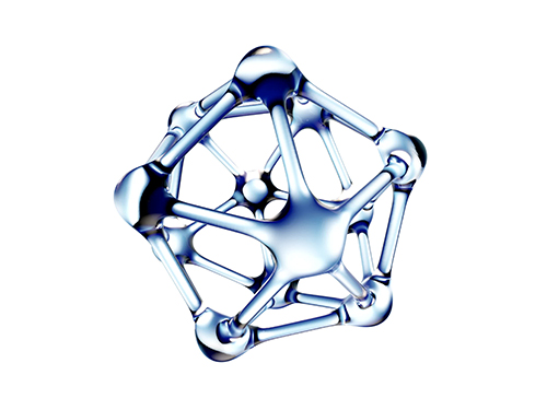 Algorithm Identifies Optimal Pairs for Composing Metal-Organic Frameworks
The integration of metal-organic frameworks (MOFs) and other metal nanoparticles has increasingly led to the creation of new multifunctional materials. Many researchers have integrated MOFs with other classes of materials to produce new structures with synergetic properties.
Despite there being over 70,000 collections of synthesized MOFs that can be used as building blocks, the precise nature of the interaction and the bonding at the interface between the two materials still remains unknown. The question is how to sort out the right matching pairs out of 70,000 MOFs.
An algorithmic study published in Nature Communications by a KAIST research team presents a clue for finding the perfect pairs. The team, led by Professor Ji-Han Kim from the Department of Chemical and Biomolecular Engineering, developed a joint computational and experimental approach to rationally design MOF@MOFs, a composite of MOFs where an MOF is grown on a different MOF.
Professor Kim’s team, in collaboration with UNIST, noted that the metal node of one MOF can coordinately bond with the linker of a different MOF and the precisely matched interface configurations at atomic and molecular levels can enhance the likelihood of synthesizing MOF@MOFs.
They screened thousands of MOFs and identified optimal MOF pairs that can seamlessly connect to one another by taking advantage of the fact that the metal node of one MOF can form coordination bonds with the linkers of the second MOF. Six pairs predicted from the computational algorithm successfully grew into single crystals.
This computational workflow can readily extend into other classes of materials and can lead to the rapid exploration of the composite MOFs arena for accelerated materials development. Even more, the workflow can enhance the likelihood of synthesizing MOF@MOFs in the form of large single crystals, and thereby demonstrated the utility of rationally designing the MOF@MOFs.
This study is the first algorithm for predicting the synthesis of composite MOFs, to the best of their knowledge. Professor Kim said, “The number of predicted pairs can increase even more with the more general 2D lattice matching, and it is worth investigating in the future.”
This study was supported by Samsung Research Funding & Incubation Center of Samsung Electronics.
(Figure: An example of a rationally synthesized MOF@MOFs (cubic HKUST-1@MOF-5 ))
2019.08.30 View 18873
Algorithm Identifies Optimal Pairs for Composing Metal-Organic Frameworks
The integration of metal-organic frameworks (MOFs) and other metal nanoparticles has increasingly led to the creation of new multifunctional materials. Many researchers have integrated MOFs with other classes of materials to produce new structures with synergetic properties.
Despite there being over 70,000 collections of synthesized MOFs that can be used as building blocks, the precise nature of the interaction and the bonding at the interface between the two materials still remains unknown. The question is how to sort out the right matching pairs out of 70,000 MOFs.
An algorithmic study published in Nature Communications by a KAIST research team presents a clue for finding the perfect pairs. The team, led by Professor Ji-Han Kim from the Department of Chemical and Biomolecular Engineering, developed a joint computational and experimental approach to rationally design MOF@MOFs, a composite of MOFs where an MOF is grown on a different MOF.
Professor Kim’s team, in collaboration with UNIST, noted that the metal node of one MOF can coordinately bond with the linker of a different MOF and the precisely matched interface configurations at atomic and molecular levels can enhance the likelihood of synthesizing MOF@MOFs.
They screened thousands of MOFs and identified optimal MOF pairs that can seamlessly connect to one another by taking advantage of the fact that the metal node of one MOF can form coordination bonds with the linkers of the second MOF. Six pairs predicted from the computational algorithm successfully grew into single crystals.
This computational workflow can readily extend into other classes of materials and can lead to the rapid exploration of the composite MOFs arena for accelerated materials development. Even more, the workflow can enhance the likelihood of synthesizing MOF@MOFs in the form of large single crystals, and thereby demonstrated the utility of rationally designing the MOF@MOFs.
This study is the first algorithm for predicting the synthesis of composite MOFs, to the best of their knowledge. Professor Kim said, “The number of predicted pairs can increase even more with the more general 2D lattice matching, and it is worth investigating in the future.”
This study was supported by Samsung Research Funding & Incubation Center of Samsung Electronics.
(Figure: An example of a rationally synthesized MOF@MOFs (cubic HKUST-1@MOF-5 ))
2019.08.30 View 18873 -
 Artificial Muscles Bloom, Dance, and Wave
Wearing a flower brooch that blooms before your eyes sounds like magic. KAIST researchers have made it real with robotic muscles.
Researchers have developed an ultrathin, artificial muscle for soft robotics. The advancement, recently reported in the journal Science Robotics, was demonstrated with a robotic blooming flower brooch, dancing robotic butterflies and fluttering tree leaves on a kinetic art piece.
The robotic equivalent of a muscle that can move is called an actuator. The actuator expands, contracts or rotates like muscle fibers using a stimulus such as electricity. Engineers around the world are striving to develop more dynamic actuators that respond quickly, can bend without breaking, and are very durable. Soft, robotic muscles could have a wide variety of applications, from wearable electronics to advanced prosthetics.
The team from KAIST’s Creative Research Initiative Center for Functionally Antagonistic Nano-Engineering developed a very thin, responsive, flexible and durable artificial muscle. The actuator looks like a skinny strip of paper about an inch long. They used a particular type of material called MXene, which is class of compounds that have layers only a few atoms thick.
Their chosen MXene material (T3C2Tx) is made of thin layers of titanium and carbon compounds. It was not flexible by itself; sheets of material would flake off the actuator when bent in a loop. That changed when the MXene was “ionically cross-linked” — connected through an ionic bond — to a synthetic polymer. The combination of materials made the actuator flexible, while still maintaining strength and conductivity, which is critical for movements driven by electricity.
Their particular combination performed better than others reported. Their actuator responded very quickly to low voltage, and lasted for more than five hours moving continuously.
To prove the tiny robotic muscle works, the team incorporated the actuator into wearable art: an origami-inspired brooch mimics how a narcissus flower unfolds its petals when a small amount of electricity is applied. They also designed robotic butterflies that move their wings up and down, and made the leaves of a tree sculpture flutter.
“Wearable robotics and kinetic art demonstrate how robotic muscles can have fun and beautiful applications,” said Il-Kwon Oh, lead paper author and professor of mechanical engineering. “It also shows the enormous potential for small, artificial muscles for a variety of uses, such as haptic feedback systems and active biomedical devices.”
The team next plans to investigate more practical applications of MXene-based soft actuators and other engineering applications of MXene 2D nanomaterials.
2019.08.22 View 27044
Artificial Muscles Bloom, Dance, and Wave
Wearing a flower brooch that blooms before your eyes sounds like magic. KAIST researchers have made it real with robotic muscles.
Researchers have developed an ultrathin, artificial muscle for soft robotics. The advancement, recently reported in the journal Science Robotics, was demonstrated with a robotic blooming flower brooch, dancing robotic butterflies and fluttering tree leaves on a kinetic art piece.
The robotic equivalent of a muscle that can move is called an actuator. The actuator expands, contracts or rotates like muscle fibers using a stimulus such as electricity. Engineers around the world are striving to develop more dynamic actuators that respond quickly, can bend without breaking, and are very durable. Soft, robotic muscles could have a wide variety of applications, from wearable electronics to advanced prosthetics.
The team from KAIST’s Creative Research Initiative Center for Functionally Antagonistic Nano-Engineering developed a very thin, responsive, flexible and durable artificial muscle. The actuator looks like a skinny strip of paper about an inch long. They used a particular type of material called MXene, which is class of compounds that have layers only a few atoms thick.
Their chosen MXene material (T3C2Tx) is made of thin layers of titanium and carbon compounds. It was not flexible by itself; sheets of material would flake off the actuator when bent in a loop. That changed when the MXene was “ionically cross-linked” — connected through an ionic bond — to a synthetic polymer. The combination of materials made the actuator flexible, while still maintaining strength and conductivity, which is critical for movements driven by electricity.
Their particular combination performed better than others reported. Their actuator responded very quickly to low voltage, and lasted for more than five hours moving continuously.
To prove the tiny robotic muscle works, the team incorporated the actuator into wearable art: an origami-inspired brooch mimics how a narcissus flower unfolds its petals when a small amount of electricity is applied. They also designed robotic butterflies that move their wings up and down, and made the leaves of a tree sculpture flutter.
“Wearable robotics and kinetic art demonstrate how robotic muscles can have fun and beautiful applications,” said Il-Kwon Oh, lead paper author and professor of mechanical engineering. “It also shows the enormous potential for small, artificial muscles for a variety of uses, such as haptic feedback systems and active biomedical devices.”
The team next plans to investigate more practical applications of MXene-based soft actuators and other engineering applications of MXene 2D nanomaterials.
2019.08.22 View 27044 -
 Research Day Highlights Most Outstanding Research Achievements
Professor Byung Jin Cho from the School of Electrical Engineering was selected as the Grand Research Prize Winner in recognition of his innovative research achievement in the fields of nano electric and flexible energy devices during the 2019 KAIST Research Day ceremony held on April 23 at the Chung Kunmo Conference Hall.
The ten most outstanding research achievements from the past year were also awarded in the three areas of Research, Innovation, Convergence Researches.
Professor Cho is an internationally recognized researcher in the field of future nano and energy device technology. Professor Cho’s team has continued to research on advanced CMOS (complementary metal-oxide semiconductors). CMOS has become his key research topic over the past three decades.
In 2014, he developed a glass fabric-based thermoelectric generator, which is extremely light and flexible and produces electricity from the heat of the human body. It is so flexible that the allowable bending radius of the generator is as low as 20 mm. There are no changes in performance even if the generator bends upward and downward for up to 120 cycles. His wearable thermoelectric generator was selected as one of the top ten most promising digital technologies by the Netexplo Forum in 2015.
He now is working on high-performance and ultra-flexible CMOS IC for biomedical applications, expanding his scope to thermal haptic technology in VR using graphene-CMOS hybrid integrated circuits; to self-powered wireless sensor nodes and self-powered ECG system using wearable thermoelectric generators .
In his special lecture at the ceremony, Professor Cho stressed the importance of collaboration in making scientific research and presented how he moved to future devices after focusing on scaling the devices.
“When I started the research on semiconductors, I focused on how to scale the device down as much as possible. For decades, we have conducted a number of procedures to produce tiny but efficient materials. Now we have shifted to develop flexible thermoelements and wearable devices,” said Professor Cho.
“We all thought the scaling down is the only way to create value-added technological breakthroughs. Now, the devices have been scaled down to 7nm and will go down to 5 nm soon. Over the past few years, I think we have gone through all the possible technological breakthroughs for reducing the size to 5nm. The semiconductor devices are made of more 1 billion transistors and go through 1,000 technological processes. So, there won’t be any possible way for a single genius to make a huge breakthrough. Without collaboration with others, it is nearly impossible to make any new technological breakthroughs.”
Professor Cho has published more than 240 papers in renowned academic journals and presented more than 300 papers at academic conferences. He has also registered approximately 50 patents in the field of semiconductor device technology.
The top ten research highlights of 2018 as follows:
- Rydberg-Atom Quantum Simulator Development by Professor Jaewook Ahn and Heung-Sun Sim from the Department of Physics
- From C-H to C-C Bonds at Room Temperature by Professor Mu-Hyun Baik from the Department of Chemistry
- The Role of Rodlike Counterions on the Interactions of DNAs by Professor Yong Woon Kim of the Graduate School of Nanoscience and Technology
- The Medal Preoptic Area Induces Hunting-Like Behaviors to Target Objects and Prey by Professor Daesoo Kim from the Department of Biological Sciences
- Identification of the Origin of Brain Tumors and New Therapeutic Strategy by Professor Jeong Ho Lee from the Graduate School of Medical Science and Engineering
- The Linear Frequency Conversion of Light at a Spatiotemporal Boundary by Professor Bumki Min from the Department of Mechanical Engineering
- An Industrial Grade Flexible Transparent Force Touch Sensor by Professor Jun-Bo Yoon from the School of Electrical Engineering
- The Detection and Clustering of Mixed-Type Defect Patterns in Wafer Bin Maps by Professor Heeyoung Kim from the Department of Industrial and Systems Engineering
- The Development of a Reconfigurable Spin-Based Logic Device by Professor Byong-Guk Park from the Department of Materials Science and Engineering
- The Development of a Miniaturized X-Ray Tube Based on Carbon Nanotube and Electronic Brachytherapy Device by Professor Sung Oh Cho from the Department of Nuclear and Quantum Engineering
Professor YongKeun Park from the Department of Physics and Professor In-Chel Park from the School of Electrical Engineering received the Research Award. For the Innovation Award, Professor Munchurl Kim from the School of Electrical Engineering was the recipient and the Convergence Research Awards was conferred to Professor Sung-Yool Choi from the School of Electrical Engineering, Professor Sung Gap Im from the Department of Chemical and Biomolecular Engineering, and Professor SangHee Park from the Department of Materials Science and Engineering during the ceremony.
For more on KAIST’s Top Research Achievements and Highlight of 2018, please refer to the attached below. click.
2019.04.25 View 18857
Research Day Highlights Most Outstanding Research Achievements
Professor Byung Jin Cho from the School of Electrical Engineering was selected as the Grand Research Prize Winner in recognition of his innovative research achievement in the fields of nano electric and flexible energy devices during the 2019 KAIST Research Day ceremony held on April 23 at the Chung Kunmo Conference Hall.
The ten most outstanding research achievements from the past year were also awarded in the three areas of Research, Innovation, Convergence Researches.
Professor Cho is an internationally recognized researcher in the field of future nano and energy device technology. Professor Cho’s team has continued to research on advanced CMOS (complementary metal-oxide semiconductors). CMOS has become his key research topic over the past three decades.
In 2014, he developed a glass fabric-based thermoelectric generator, which is extremely light and flexible and produces electricity from the heat of the human body. It is so flexible that the allowable bending radius of the generator is as low as 20 mm. There are no changes in performance even if the generator bends upward and downward for up to 120 cycles. His wearable thermoelectric generator was selected as one of the top ten most promising digital technologies by the Netexplo Forum in 2015.
He now is working on high-performance and ultra-flexible CMOS IC for biomedical applications, expanding his scope to thermal haptic technology in VR using graphene-CMOS hybrid integrated circuits; to self-powered wireless sensor nodes and self-powered ECG system using wearable thermoelectric generators .
In his special lecture at the ceremony, Professor Cho stressed the importance of collaboration in making scientific research and presented how he moved to future devices after focusing on scaling the devices.
“When I started the research on semiconductors, I focused on how to scale the device down as much as possible. For decades, we have conducted a number of procedures to produce tiny but efficient materials. Now we have shifted to develop flexible thermoelements and wearable devices,” said Professor Cho.
“We all thought the scaling down is the only way to create value-added technological breakthroughs. Now, the devices have been scaled down to 7nm and will go down to 5 nm soon. Over the past few years, I think we have gone through all the possible technological breakthroughs for reducing the size to 5nm. The semiconductor devices are made of more 1 billion transistors and go through 1,000 technological processes. So, there won’t be any possible way for a single genius to make a huge breakthrough. Without collaboration with others, it is nearly impossible to make any new technological breakthroughs.”
Professor Cho has published more than 240 papers in renowned academic journals and presented more than 300 papers at academic conferences. He has also registered approximately 50 patents in the field of semiconductor device technology.
The top ten research highlights of 2018 as follows:
- Rydberg-Atom Quantum Simulator Development by Professor Jaewook Ahn and Heung-Sun Sim from the Department of Physics
- From C-H to C-C Bonds at Room Temperature by Professor Mu-Hyun Baik from the Department of Chemistry
- The Role of Rodlike Counterions on the Interactions of DNAs by Professor Yong Woon Kim of the Graduate School of Nanoscience and Technology
- The Medal Preoptic Area Induces Hunting-Like Behaviors to Target Objects and Prey by Professor Daesoo Kim from the Department of Biological Sciences
- Identification of the Origin of Brain Tumors and New Therapeutic Strategy by Professor Jeong Ho Lee from the Graduate School of Medical Science and Engineering
- The Linear Frequency Conversion of Light at a Spatiotemporal Boundary by Professor Bumki Min from the Department of Mechanical Engineering
- An Industrial Grade Flexible Transparent Force Touch Sensor by Professor Jun-Bo Yoon from the School of Electrical Engineering
- The Detection and Clustering of Mixed-Type Defect Patterns in Wafer Bin Maps by Professor Heeyoung Kim from the Department of Industrial and Systems Engineering
- The Development of a Reconfigurable Spin-Based Logic Device by Professor Byong-Guk Park from the Department of Materials Science and Engineering
- The Development of a Miniaturized X-Ray Tube Based on Carbon Nanotube and Electronic Brachytherapy Device by Professor Sung Oh Cho from the Department of Nuclear and Quantum Engineering
Professor YongKeun Park from the Department of Physics and Professor In-Chel Park from the School of Electrical Engineering received the Research Award. For the Innovation Award, Professor Munchurl Kim from the School of Electrical Engineering was the recipient and the Convergence Research Awards was conferred to Professor Sung-Yool Choi from the School of Electrical Engineering, Professor Sung Gap Im from the Department of Chemical and Biomolecular Engineering, and Professor SangHee Park from the Department of Materials Science and Engineering during the ceremony.
For more on KAIST’s Top Research Achievements and Highlight of 2018, please refer to the attached below. click.
2019.04.25 View 18857 -
 True-meaning Wearable Displays: Self-powered, Washable and Wearable
(Video: The washing process of wearing display module) When we think about clothes, they are usually formed with textiles and have to be both wearable and washable for daily use; however, smart clothing has had a problem with its power sources and moisture permeability, which causes the devices to malfunction. This problem has now been overcome by a KAIST research team, who developed a textile-based wearable display module technology that is washable and does not require an external power source.
To ease out the problem of external power sources and enhance the practicability of wearable displays, Professor Kyung Cheol Choi from the School of Electrical Engineering and his team fabricated their wearing display modules on real textiles that integrated polymer solar cells (PSCs) with organic light emitting diodes (OLEDs).
PSCs have been one of the most promising candidates for a next-generation power source, especially for wearable and optoelectronic applications because they can provide stable power without an external power source, while OLEDs can be driven with milliwatts. However, the problem was that they are both very vulnerable to external moisture and oxygen. The encapsulation barrier is essential for their reliability. The conventional encapsulation barrier is sufficient for normal environments; however, it loses its characteristics in aqueous environments, such as water. It limits the commercialization of wearing displays that must operate even on rainy days or after washing.
To tackle this issue, the team employed a washable encapsulation barrier that can protect the device without losing its characteristics after washing through atomic layer deposition (ALD) and spin coating. With this encapsulation technology, the team confirmed that textile-based wearing display modules including PSCs, OLEDs, and the proposed encapsulation barrier exhibited little change in characteristics even after 20 washings with 10-minute cycles. Moreover, the encapsulated device operated stably with a low curvature radius of 3mm and boasted high reliability.
Finally, it exhibited no deterioration in properties over 30 days even after being subjected to both bending stress and washing. Since it uses a less stressful textile, compared to conventional wearable electronic devices that use traditional plastic substrates, this technology can accelerate the commercialization of wearing electronic devices. Importantly, this wearable electronic device in daily life can save energy through a self-powered system.
Professor Choi said, “I could say that this research realized a truly washable wearable electronic module in the sense that it uses daily wearable textiles instead of the plastic used in conventional wearable electronic devices. Saving energy with PSCs, it can be self-powered, using nature-friendly solar energy, and washed. I believe that it has paved the way for a ‘true-meaning wearable display’ that can be formed on textile, beyond the attachable form of wearable technology.”
This research, in collaboration with Professor Seok Ho Cho from Chonnam National University and led by Eun Gyo Jeong, was published in Energy and Environmental Science (10.1039/c8ee03271h) on January 18, 2019.
Figure 1. Schematic and photo of a washable wearing display module
Figure 2. Cover page of Energy and Environmental Science
2019.03.21 View 32671
True-meaning Wearable Displays: Self-powered, Washable and Wearable
(Video: The washing process of wearing display module) When we think about clothes, they are usually formed with textiles and have to be both wearable and washable for daily use; however, smart clothing has had a problem with its power sources and moisture permeability, which causes the devices to malfunction. This problem has now been overcome by a KAIST research team, who developed a textile-based wearable display module technology that is washable and does not require an external power source.
To ease out the problem of external power sources and enhance the practicability of wearable displays, Professor Kyung Cheol Choi from the School of Electrical Engineering and his team fabricated their wearing display modules on real textiles that integrated polymer solar cells (PSCs) with organic light emitting diodes (OLEDs).
PSCs have been one of the most promising candidates for a next-generation power source, especially for wearable and optoelectronic applications because they can provide stable power without an external power source, while OLEDs can be driven with milliwatts. However, the problem was that they are both very vulnerable to external moisture and oxygen. The encapsulation barrier is essential for their reliability. The conventional encapsulation barrier is sufficient for normal environments; however, it loses its characteristics in aqueous environments, such as water. It limits the commercialization of wearing displays that must operate even on rainy days or after washing.
To tackle this issue, the team employed a washable encapsulation barrier that can protect the device without losing its characteristics after washing through atomic layer deposition (ALD) and spin coating. With this encapsulation technology, the team confirmed that textile-based wearing display modules including PSCs, OLEDs, and the proposed encapsulation barrier exhibited little change in characteristics even after 20 washings with 10-minute cycles. Moreover, the encapsulated device operated stably with a low curvature radius of 3mm and boasted high reliability.
Finally, it exhibited no deterioration in properties over 30 days even after being subjected to both bending stress and washing. Since it uses a less stressful textile, compared to conventional wearable electronic devices that use traditional plastic substrates, this technology can accelerate the commercialization of wearing electronic devices. Importantly, this wearable electronic device in daily life can save energy through a self-powered system.
Professor Choi said, “I could say that this research realized a truly washable wearable electronic module in the sense that it uses daily wearable textiles instead of the plastic used in conventional wearable electronic devices. Saving energy with PSCs, it can be self-powered, using nature-friendly solar energy, and washed. I believe that it has paved the way for a ‘true-meaning wearable display’ that can be formed on textile, beyond the attachable form of wearable technology.”
This research, in collaboration with Professor Seok Ho Cho from Chonnam National University and led by Eun Gyo Jeong, was published in Energy and Environmental Science (10.1039/c8ee03271h) on January 18, 2019.
Figure 1. Schematic and photo of a washable wearing display module
Figure 2. Cover page of Energy and Environmental Science
2019.03.21 View 32671