research
-
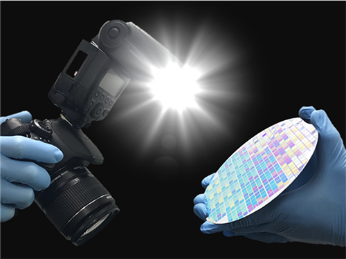 Semiconductor Patterning of Seven Nanometers Technology Using a Camera Flash
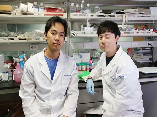
A research team led by Professor Sang Ouk Kim in the Department of Materials Science and Engineering at KAIST has developed semiconductor manufacturing technology using a camera flash.
This technology can manufacture ultra-fine patterns over a large area by irradiating a single flash with a seven-nanometer patterning technique for semiconductors. It can facilitate the manufacturing of highly efficient, integrated semiconductor devices in the future.
Technology for the Artificial Intelligence (AI), the Internet of Things (IoTs), and big data, which are the major keys for the fourth Industrial Revolution, require high-capacity, high-performance semiconductor devices. It is necessary to develop lithography technology to produce such next-generation, highly integrated semiconductor devices.
Although related industries have been using conventional photolithography for small patterns, this technique has limitations for forming a pattern of sub-10 nm patterns.
Molecular assembly patterning technology using polymers has been in the spotlight as the next generation technology to replace photolithography because it is inexpensive to produce and can easily form sub-10 nm patterns. However, since it generally takes a long time for heat treatment at high-temperature or toxic solvent vapor treatment, mass production is difficult and thus its commercialization has been limited.
The research team introduced a camera flash that instantly emits strong light to solve the issues of polymer molecular assembly patterning. Using a flash can possibly achieve a semiconductor patterning of seven nanometers within 15 milliseconds (1 millisecond = 1/1,000 second), which can generate a temperature of several hundred degrees Celsius in several tens of milliseconds.
The team has demonstrated that applying this technology to polymer molecular assembly allows a single flash of light to form molecular assembly patterns.
The team also identified its compatibility with polymer flexible substrates, which are impossible to process at high temperatures. Through these findings, the technology can be applied to the fabrication of next-generation, flexible semiconductors.
The researchers said the camera flash photo-thermal process will be introduced into molecular assembly technology and this highly-efficiency technology can accelerate the realization of molecular assembly semiconductor technology.
Professor Kim, who led the research, said, “Despite its potential, molecular assembly semiconductor technology has remained a big challenge in improving process efficiency.” “This technology will be a breakthrough for the practical use of molecular assembly-based semiconductors.”
The paper was published in the international journal, Advanced Materials on August 21 with first authors, researcher Hyeong Min Jin and PhD candidate Dae Yong Park.
The research, sponsored by the Ministry of Science and ICT, was co-led Professor by Keon Jae Lee in the Department of Materials Science and Engineering at KAIST, and Professor Kwang Ho Kim in the School of Materials Science and Engineering at Pusan National University.
(1. Formation of semiconductor patterns using a camera flash)
(Schematic diagram of molecular assembly pattern using a camera flash)
(Self-assembled patterns)
2017.09.18 View 12157
Semiconductor Patterning of Seven Nanometers Technology Using a Camera Flash
A research team led by Professor Sang Ouk Kim in the Department of Materials Science and Engineering at KAIST has developed semiconductor manufacturing technology using a camera flash.
This technology can manufacture ultra-fine patterns over a large area by irradiating a single flash with a seven-nanometer patterning technique for semiconductors. It can facilitate the manufacturing of highly efficient, integrated semiconductor devices in the future.
Technology for the Artificial Intelligence (AI), the Internet of Things (IoTs), and big data, which are the major keys for the fourth Industrial Revolution, require high-capacity, high-performance semiconductor devices. It is necessary to develop lithography technology to produce such next-generation, highly integrated semiconductor devices.
Although related industries have been using conventional photolithography for small patterns, this technique has limitations for forming a pattern of sub-10 nm patterns.
Molecular assembly patterning technology using polymers has been in the spotlight as the next generation technology to replace photolithography because it is inexpensive to produce and can easily form sub-10 nm patterns. However, since it generally takes a long time for heat treatment at high-temperature or toxic solvent vapor treatment, mass production is difficult and thus its commercialization has been limited.
The research team introduced a camera flash that instantly emits strong light to solve the issues of polymer molecular assembly patterning. Using a flash can possibly achieve a semiconductor patterning of seven nanometers within 15 milliseconds (1 millisecond = 1/1,000 second), which can generate a temperature of several hundred degrees Celsius in several tens of milliseconds.
The team has demonstrated that applying this technology to polymer molecular assembly allows a single flash of light to form molecular assembly patterns.
The team also identified its compatibility with polymer flexible substrates, which are impossible to process at high temperatures. Through these findings, the technology can be applied to the fabrication of next-generation, flexible semiconductors.
The researchers said the camera flash photo-thermal process will be introduced into molecular assembly technology and this highly-efficiency technology can accelerate the realization of molecular assembly semiconductor technology.
Professor Kim, who led the research, said, “Despite its potential, molecular assembly semiconductor technology has remained a big challenge in improving process efficiency.” “This technology will be a breakthrough for the practical use of molecular assembly-based semiconductors.”
The paper was published in the international journal, Advanced Materials on August 21 with first authors, researcher Hyeong Min Jin and PhD candidate Dae Yong Park.
The research, sponsored by the Ministry of Science and ICT, was co-led Professor by Keon Jae Lee in the Department of Materials Science and Engineering at KAIST, and Professor Kwang Ho Kim in the School of Materials Science and Engineering at Pusan National University.
(1. Formation of semiconductor patterns using a camera flash)
(Schematic diagram of molecular assembly pattern using a camera flash)
(Self-assembled patterns)
2017.09.18 View 12157 -
 A Novel and Practical Fab-route for Superomniphobic Liquid-free Surfaces
(clockwise from left: Jaeho Choi, Hee Tak Kim, Shin-Hyun Kim)
A joint research team led by Professor Hee Tak Kim and Shin-Hyun Kim in the Department of Chemical and Biomolecular Engineering at KAIST developed a fabrication technology that can inexpensively produce surfaces capable of repelling liquids, including water and oil.
The team used the photofluidization of azobenzene molecule-containing polymers to generate a superomniphobic surface which can be applied for developing stain-free fabrics, non-biofouling medical tubing, and corrosion-free surfaces.
Mushroom-shaped surface textures, also called doubly re-entrant structures, are known to be the most effective surface structure that enhances resistance against liquid invasion, thereby exhibiting superior superomniphobic property.
However, the existing procedures for their fabrication are highly delicate, time-consuming, and costly. Moreover, the materials required for the fabrication are restricted to an inflexible and expensive silicon wafer, which limits the practical use of the surface.
To overcome such limitations, the research team used a different approach to fabricate the re-entrant structures called localized photofludization by using the peculiar optical phenomenon of azobenzene molecule-containing polymers (referred to as azopolymers). It is a phenomenon where an azopolymer becomes fluidized under irradiation, and the fluidization takes place locally within the thin surface layer of the azopolymer.
With this novel approach, the team facilitated the localized photofluidization in the top surface layer of azopolymer cylindrical posts, successfully reconfiguring the cylindrical posts to doubly re-entrant geometry while the fluidized thin top surface of an azopolymer is flowing down.
The structure developed by the team exhibits a superior superomniphobic property even for liquids infiltrating the surface immediately.
Moreover, the superomniphobic property can be maintained on a curved target surface because its surficial materials are based on high molecules.
Furthermore, the fabrication procedure of the structure is highly reproducible and scalable, providing a practical route to creating robust omniphobic surfaces.
Professor Hee Tak Kim said, “Not only does the novel photo-fluidization technology in this study produce superior superomniphobic surfaces, but it also possesses many practical advantages in terms of fab-procedures and material flexibility; therefore, it could greatly contribute to real uses in diverse applications.”
Professor Shin-Hyun Kim added, “The designed doubly re-entrant geometry in this study was inspired by the skin structure of springtails, insects dwelling in soil that breathe through their skin. As I carried out this research, I once again realized that humans can learn from nature to create new engineering designs.”
The paper (Jaeho Choi as a first author) was published in ACS Nano, an international journal for Nano-technology, in August.
(Schematic diagram of mushroom-shaped structure fabrication)
(SEM image of mushroom-shaped structure)
(Image of superomniphobic property of different types of liquid)
2017.09.08 View 8199
A Novel and Practical Fab-route for Superomniphobic Liquid-free Surfaces
(clockwise from left: Jaeho Choi, Hee Tak Kim, Shin-Hyun Kim)
A joint research team led by Professor Hee Tak Kim and Shin-Hyun Kim in the Department of Chemical and Biomolecular Engineering at KAIST developed a fabrication technology that can inexpensively produce surfaces capable of repelling liquids, including water and oil.
The team used the photofluidization of azobenzene molecule-containing polymers to generate a superomniphobic surface which can be applied for developing stain-free fabrics, non-biofouling medical tubing, and corrosion-free surfaces.
Mushroom-shaped surface textures, also called doubly re-entrant structures, are known to be the most effective surface structure that enhances resistance against liquid invasion, thereby exhibiting superior superomniphobic property.
However, the existing procedures for their fabrication are highly delicate, time-consuming, and costly. Moreover, the materials required for the fabrication are restricted to an inflexible and expensive silicon wafer, which limits the practical use of the surface.
To overcome such limitations, the research team used a different approach to fabricate the re-entrant structures called localized photofludization by using the peculiar optical phenomenon of azobenzene molecule-containing polymers (referred to as azopolymers). It is a phenomenon where an azopolymer becomes fluidized under irradiation, and the fluidization takes place locally within the thin surface layer of the azopolymer.
With this novel approach, the team facilitated the localized photofluidization in the top surface layer of azopolymer cylindrical posts, successfully reconfiguring the cylindrical posts to doubly re-entrant geometry while the fluidized thin top surface of an azopolymer is flowing down.
The structure developed by the team exhibits a superior superomniphobic property even for liquids infiltrating the surface immediately.
Moreover, the superomniphobic property can be maintained on a curved target surface because its surficial materials are based on high molecules.
Furthermore, the fabrication procedure of the structure is highly reproducible and scalable, providing a practical route to creating robust omniphobic surfaces.
Professor Hee Tak Kim said, “Not only does the novel photo-fluidization technology in this study produce superior superomniphobic surfaces, but it also possesses many practical advantages in terms of fab-procedures and material flexibility; therefore, it could greatly contribute to real uses in diverse applications.”
Professor Shin-Hyun Kim added, “The designed doubly re-entrant geometry in this study was inspired by the skin structure of springtails, insects dwelling in soil that breathe through their skin. As I carried out this research, I once again realized that humans can learn from nature to create new engineering designs.”
The paper (Jaeho Choi as a first author) was published in ACS Nano, an international journal for Nano-technology, in August.
(Schematic diagram of mushroom-shaped structure fabrication)
(SEM image of mushroom-shaped structure)
(Image of superomniphobic property of different types of liquid)
2017.09.08 View 8199 -
 Discovery of an Optimal Drug Combination: Overcoming Resistance to Targeted Drugs for Liver Cancer
A KAIST research team presented a novel method for improving medication treatment for liver cancer using Systems Biology, combining research from information technology and the life sciences. Professor Kwang-Hyun Cho in the Department of Bio and Brain Engineering at KAIST conducted the research in collaboration with Professor Jung-Hwan Yoon in the Department of Internal Medicine at Seoul National University Hospital. This research was published in Hepatology in September 2017 (available online from August 24, 2017).
Liver cancer is the fifth and seventh most common cancer found in men and women throughout the world, which places it second in the cause of cancer deaths. In particular, Korea has 28.4 deaths from liver cancer per 100,000 persons, the highest death rate among OECD countries and twice that of Japan.
Each year in Korea, 16,000 people get liver cancer on average, yet the five-year survival rate stands below 12%. According to the National Cancer Information Center, lung cancer (17,399) took the highest portion of cancer-related deaths, followed by liver cancer (11,311) based on last year data.
Liver cancer is known to carry the highest social cost in comparison to other cancers and it causes the highest fatality in earlier age groups (40s-50s). In that sense, it is necessary to develop a new treatment that mitigates side effects yet elevates the survival rate.
There are ways in which liver cancer can be cured, such as surgery, embolization, and medication treatments; however, the options become limited for curing progressive cancer, a stage in which surgical methods cannot be executed.
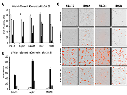
Among anticancer medications, Sorafenib, a drug known for enhancing the survival rate of cancer patients, is a unique drug allowed for use as a targeted anticancer medication for progressive liver cancer patients. Its sales reached more than ten billion KRW annually in Korea, but its efficacy works on only about 20% of the treated patients. Also, acquired resistance to Sorafenib is emerging. Additionally, the action mechanism and resistance mechanism of Sorafenib is only vaguely identified.Although Sorafenib only extends the survival rate of terminal cancer patients less than three months on average, it is widely being used because drugs developed by global pharmaceutical companies failed to outperform its effectiveness.
Professor Cho’s research team analyzed the expression changes of genes in cell lines in response to Sorafenib in order to identify the effect and the resistance mechanism of Sorafenib.
As a result, the team discovered the resistance mechanism of Sorafenib using Systems Biology analysis. By combining computer simulations and biological experiments, it was revealed that protein disulfide isomerase (PDI) plays a crucial role in the resistance mechanism of Sorafenib and that its efficacy can be improved significantly by blocking PDI.
The research team used mice in the experiment and discovered the synergic effect of PDI inhibition with Sorafenib for reducing liver cancer cells, known as hepatocellular carcinoma. Also, more PDIs are shown in tissue from patients who possess a resistance to Sorafenib. From these findings, the team could identify the possibility of its clinical applications. The team also confirmed these findings from clinical data through a retrospective cohort study.
“Molecules that play an important role in cell lines are mostly put under complex regulation. For this reason, the existing biological research has a fundamental limitations for discovering its underlying principles,” Professor Cho said. “This research is a representative case of overcoming this limitation of traditional life science research by using a Systems Biology approach, combining IT and life science. It suggests the possibility of developing a new method that overcomes drug resistance with a network analysis of the targeted drug action mechanism of cancer.”
The research was supported by the National Research Foundation of Korea (NRF) and funded by the Ministry of Science and ICT.
(Figure 1. Simulation results from cellular experiments using hepatocellular carcinoma)
(Figure 2. Network analysis and computer simulation by using the endoplasmic reticulum (ER) stress network)
(Figure 3. ER stress network model)
2017.08.30 View 12939
Discovery of an Optimal Drug Combination: Overcoming Resistance to Targeted Drugs for Liver Cancer
A KAIST research team presented a novel method for improving medication treatment for liver cancer using Systems Biology, combining research from information technology and the life sciences. Professor Kwang-Hyun Cho in the Department of Bio and Brain Engineering at KAIST conducted the research in collaboration with Professor Jung-Hwan Yoon in the Department of Internal Medicine at Seoul National University Hospital. This research was published in Hepatology in September 2017 (available online from August 24, 2017).
Liver cancer is the fifth and seventh most common cancer found in men and women throughout the world, which places it second in the cause of cancer deaths. In particular, Korea has 28.4 deaths from liver cancer per 100,000 persons, the highest death rate among OECD countries and twice that of Japan.
Each year in Korea, 16,000 people get liver cancer on average, yet the five-year survival rate stands below 12%. According to the National Cancer Information Center, lung cancer (17,399) took the highest portion of cancer-related deaths, followed by liver cancer (11,311) based on last year data.
Liver cancer is known to carry the highest social cost in comparison to other cancers and it causes the highest fatality in earlier age groups (40s-50s). In that sense, it is necessary to develop a new treatment that mitigates side effects yet elevates the survival rate.
There are ways in which liver cancer can be cured, such as surgery, embolization, and medication treatments; however, the options become limited for curing progressive cancer, a stage in which surgical methods cannot be executed.
Among anticancer medications, Sorafenib, a drug known for enhancing the survival rate of cancer patients, is a unique drug allowed for use as a targeted anticancer medication for progressive liver cancer patients. Its sales reached more than ten billion KRW annually in Korea, but its efficacy works on only about 20% of the treated patients. Also, acquired resistance to Sorafenib is emerging. Additionally, the action mechanism and resistance mechanism of Sorafenib is only vaguely identified.Although Sorafenib only extends the survival rate of terminal cancer patients less than three months on average, it is widely being used because drugs developed by global pharmaceutical companies failed to outperform its effectiveness.
Professor Cho’s research team analyzed the expression changes of genes in cell lines in response to Sorafenib in order to identify the effect and the resistance mechanism of Sorafenib.
As a result, the team discovered the resistance mechanism of Sorafenib using Systems Biology analysis. By combining computer simulations and biological experiments, it was revealed that protein disulfide isomerase (PDI) plays a crucial role in the resistance mechanism of Sorafenib and that its efficacy can be improved significantly by blocking PDI.
The research team used mice in the experiment and discovered the synergic effect of PDI inhibition with Sorafenib for reducing liver cancer cells, known as hepatocellular carcinoma. Also, more PDIs are shown in tissue from patients who possess a resistance to Sorafenib. From these findings, the team could identify the possibility of its clinical applications. The team also confirmed these findings from clinical data through a retrospective cohort study.
“Molecules that play an important role in cell lines are mostly put under complex regulation. For this reason, the existing biological research has a fundamental limitations for discovering its underlying principles,” Professor Cho said. “This research is a representative case of overcoming this limitation of traditional life science research by using a Systems Biology approach, combining IT and life science. It suggests the possibility of developing a new method that overcomes drug resistance with a network analysis of the targeted drug action mechanism of cancer.”
The research was supported by the National Research Foundation of Korea (NRF) and funded by the Ministry of Science and ICT.
(Figure 1. Simulation results from cellular experiments using hepatocellular carcinoma)
(Figure 2. Network analysis and computer simulation by using the endoplasmic reticulum (ER) stress network)
(Figure 3. ER stress network model)
2017.08.30 View 12939 -
 The Medici Effect: Highly Flexible, Wearable Displays Born in KAIST
(Ph.D. candidate Seungyeop Choi)
How do you feel when technology you saw in a movie is made into reality? Collaboration between the electrical engineering and textile industries has made TVs or smartphone screens displaying on clothing a reality.
A research team led by Professor Kyung Cheol Choi at the School of Electrical Engineering presented wearable displays for various applications including fashion, IT, and healthcare. Integrating OLED (organic light-emitting diode) into fabrics, the team developed the most highly flexible and reliable technology for wearable displays in the world.
Recently, information displays have become increasingly important as they construct the external part of smart devices for the next generation. As world trends are focusing on the Internet of Things (IoTs) and wearable technology, the team drew a lot of attention by making great progress towards commercializing clothing-shaped ‘wearable displays’.
The research for realizing displays on clothing gained considerable attention from academia as well as industry when research on luminescence formed in fabrics was introduced in 2011; however, there was no technology for commercializing it due to its surface roughness and flexibility.
Because of this technical limitation, clothing-shaped wearable displays were thought to be unreachable technology. However, the KAIST team recently succeeded in developing the world’s most highly efficient, light-emitting clothes that can be commercialized.
The research team used two different approaches, fabric-type and fiber-type, in order to realize clothing-shaped wearable displays. In 2015, the team successfully laminated a thin planarization sheet thermally onto fabric to form a surface that is compatible with the OLEDs approximately 200 hundred nanometers thick. Also, the team reported their research outcomes on enhancing the reliability of operating fiber-based OLEDs. In 2016, the team introduced a dip-coating method, capable of uniformly depositing layers, to develop polymer light-emitting diodes, which show high luminance even on thin fabric.
Based on the research performance in 2015 and 2016, Ph.D. candidate Seungyeop Choi took the lead in the research team and succeeded in realizing fabric-based OLEDs, showing high luminance and efficiency while maintaining the flexibility of the fabric.
The long-term reliability of this wearable device that has the world’s best electrical and optical characteristics was verified through their self-developed, organic and inorganic encapsulation technology. According to the team, their wearable device facilitates the operation of OLEDs even at a bending radius of 2mm.
According to Choi, “Having wavy structures and empty spaces, fiber plays a significant role in lowering the mechanical stress on the OLEDs.”
“Screen displayed on our daily clothing is no longer a future technology,” said Professor Choi. “Light-emitting clothes will have considerable influence on not only the e-textile industry but also the automobile and healthcare industries.”
Moreover, the research team remarked, “It means a lot to realize clothing-shaped OLEDs that have the world’s best luminance and efficiency. It is the most flexible fabric-based light-emitting device among those reported. Moreover, noting that this research carried out an in-depth analysis of the mechanical characteristics of the clothing-spared, light-emitting device, the research performance will become a guideline for developing the fabric-based electronics industry.”
This research was funded by the Ministry of Trade, Industry and Energy and collaborated with KOLON Glotech, INC. The research performance was published in Scientific Reports in July.
(OLEDs operating in fabrics)
(Current-voltage-luminance and efficiency of the highly flexible, fabric-based OLEDs;Image of OLEDs after repetitive bending tests;Verification of flexibility through mechanical simulation)
2017.08.24 View 16433
The Medici Effect: Highly Flexible, Wearable Displays Born in KAIST
(Ph.D. candidate Seungyeop Choi)
How do you feel when technology you saw in a movie is made into reality? Collaboration between the electrical engineering and textile industries has made TVs or smartphone screens displaying on clothing a reality.
A research team led by Professor Kyung Cheol Choi at the School of Electrical Engineering presented wearable displays for various applications including fashion, IT, and healthcare. Integrating OLED (organic light-emitting diode) into fabrics, the team developed the most highly flexible and reliable technology for wearable displays in the world.
Recently, information displays have become increasingly important as they construct the external part of smart devices for the next generation. As world trends are focusing on the Internet of Things (IoTs) and wearable technology, the team drew a lot of attention by making great progress towards commercializing clothing-shaped ‘wearable displays’.
The research for realizing displays on clothing gained considerable attention from academia as well as industry when research on luminescence formed in fabrics was introduced in 2011; however, there was no technology for commercializing it due to its surface roughness and flexibility.
Because of this technical limitation, clothing-shaped wearable displays were thought to be unreachable technology. However, the KAIST team recently succeeded in developing the world’s most highly efficient, light-emitting clothes that can be commercialized.
The research team used two different approaches, fabric-type and fiber-type, in order to realize clothing-shaped wearable displays. In 2015, the team successfully laminated a thin planarization sheet thermally onto fabric to form a surface that is compatible with the OLEDs approximately 200 hundred nanometers thick. Also, the team reported their research outcomes on enhancing the reliability of operating fiber-based OLEDs. In 2016, the team introduced a dip-coating method, capable of uniformly depositing layers, to develop polymer light-emitting diodes, which show high luminance even on thin fabric.
Based on the research performance in 2015 and 2016, Ph.D. candidate Seungyeop Choi took the lead in the research team and succeeded in realizing fabric-based OLEDs, showing high luminance and efficiency while maintaining the flexibility of the fabric.
The long-term reliability of this wearable device that has the world’s best electrical and optical characteristics was verified through their self-developed, organic and inorganic encapsulation technology. According to the team, their wearable device facilitates the operation of OLEDs even at a bending radius of 2mm.
According to Choi, “Having wavy structures and empty spaces, fiber plays a significant role in lowering the mechanical stress on the OLEDs.”
“Screen displayed on our daily clothing is no longer a future technology,” said Professor Choi. “Light-emitting clothes will have considerable influence on not only the e-textile industry but also the automobile and healthcare industries.”
Moreover, the research team remarked, “It means a lot to realize clothing-shaped OLEDs that have the world’s best luminance and efficiency. It is the most flexible fabric-based light-emitting device among those reported. Moreover, noting that this research carried out an in-depth analysis of the mechanical characteristics of the clothing-spared, light-emitting device, the research performance will become a guideline for developing the fabric-based electronics industry.”
This research was funded by the Ministry of Trade, Industry and Energy and collaborated with KOLON Glotech, INC. The research performance was published in Scientific Reports in July.
(OLEDs operating in fabrics)
(Current-voltage-luminance and efficiency of the highly flexible, fabric-based OLEDs;Image of OLEDs after repetitive bending tests;Verification of flexibility through mechanical simulation)
2017.08.24 View 16433 -
 Solutal Marangoni Flows of Miscible Liquid Drive Transport without Surface Contamination
(Professor Hyoungsoo Kim, Department of Mechanical Engineering, KAIST)
A research team led by Hyoungsoo Kim, a professor of Mechanical Engineering at KAIST, succeeded in quantifying the phenomenon called, the Marangoni effect, which occurs at the interface between alcohol and water. It is expected that this finding will be a valuable resource used for effectively removing impurities from a surface fluid without any contamination, and developing materials that can replace surfactants.
This research, co-conducted with a research team led by Professor Howard A. Stone at Princeton University, was published online in Nature Physics on July 31.
The Marangoni effect, also known as tears of wine, is generated when two fluids having a different surface tension meet, causing finite mixing, spreading time and length scale. Typically, people believe that infinitely miscible liquids immediately mix together; however, it is not always true according to this paper.
The typical surface tension of alcohol is three times lower than that of water, and this different surface tension generates the Marangoni-driven convection flow at the interface of the two liquids. In addition, there is a certain amount of time required for them to mix.
This phenomenon has been discussed many times since it was discovered in early the 20th century, yet there was a limit to quantifying and explaining it.
Professor Kim, considering the mixing and spreading mechanism, used various flow visualization techniques and equipment for capturing high speed images in his experiment.
Through the flow visualization methods, the team succeeded in quantifying and explaining the complex, physicochemical phenomenon generated between water and alcohol. Moreover, they developed a theoretical model to predict the physicochemical hydrodynamic phenomena.
The theoretical model can predict the speed of Marangoni-driven convection flow, the area of a drop of alcohol and the time required to develop the flow field. Hence, this model can map out types of materials (e.g., alcohol) and the volume of a drop of liquid as applicable to target a specific situation.
Moreover, the research team believes that the interfacial flow enables the driving of bulk flows and that it can be a source of technology for effectively delivering drugs and removing impurities from a surface of substance without causing secondary contamination.
Above all, the results show a possibility for replacing surfactant with alcohol as a material used for delivering drugs. In the case of the drug delivery, some drugs are encapsulated with a surfactant in order to be effectively transported in vivo; however, the surfactant accumulates in the body, which can cause various side effects, such as heart disease. Therefore, using new materials like alcohol for drug delivery will contribute to preventing the side effects caused by the surfactant.
“The surfactant is used for delivering drugs, but it is difficult to be expelled from the body. This will cause various side effects, such as heart diseases in asthmatic patients,” said Professor Kim. “I hope that using new materials, like alcohol, will free people from these side effects.”
(Marangoni-driven convection flow generated at the interface between water and alcohol, and the flow visualization results)
- A drop of alcohol on a water surface
- Comparison of mixing structures on the surface
- Marangoni mixing flow under the free surface
2017.08.18 View 9130
Solutal Marangoni Flows of Miscible Liquid Drive Transport without Surface Contamination
(Professor Hyoungsoo Kim, Department of Mechanical Engineering, KAIST)
A research team led by Hyoungsoo Kim, a professor of Mechanical Engineering at KAIST, succeeded in quantifying the phenomenon called, the Marangoni effect, which occurs at the interface between alcohol and water. It is expected that this finding will be a valuable resource used for effectively removing impurities from a surface fluid without any contamination, and developing materials that can replace surfactants.
This research, co-conducted with a research team led by Professor Howard A. Stone at Princeton University, was published online in Nature Physics on July 31.
The Marangoni effect, also known as tears of wine, is generated when two fluids having a different surface tension meet, causing finite mixing, spreading time and length scale. Typically, people believe that infinitely miscible liquids immediately mix together; however, it is not always true according to this paper.
The typical surface tension of alcohol is three times lower than that of water, and this different surface tension generates the Marangoni-driven convection flow at the interface of the two liquids. In addition, there is a certain amount of time required for them to mix.
This phenomenon has been discussed many times since it was discovered in early the 20th century, yet there was a limit to quantifying and explaining it.
Professor Kim, considering the mixing and spreading mechanism, used various flow visualization techniques and equipment for capturing high speed images in his experiment.
Through the flow visualization methods, the team succeeded in quantifying and explaining the complex, physicochemical phenomenon generated between water and alcohol. Moreover, they developed a theoretical model to predict the physicochemical hydrodynamic phenomena.
The theoretical model can predict the speed of Marangoni-driven convection flow, the area of a drop of alcohol and the time required to develop the flow field. Hence, this model can map out types of materials (e.g., alcohol) and the volume of a drop of liquid as applicable to target a specific situation.
Moreover, the research team believes that the interfacial flow enables the driving of bulk flows and that it can be a source of technology for effectively delivering drugs and removing impurities from a surface of substance without causing secondary contamination.
Above all, the results show a possibility for replacing surfactant with alcohol as a material used for delivering drugs. In the case of the drug delivery, some drugs are encapsulated with a surfactant in order to be effectively transported in vivo; however, the surfactant accumulates in the body, which can cause various side effects, such as heart disease. Therefore, using new materials like alcohol for drug delivery will contribute to preventing the side effects caused by the surfactant.
“The surfactant is used for delivering drugs, but it is difficult to be expelled from the body. This will cause various side effects, such as heart diseases in asthmatic patients,” said Professor Kim. “I hope that using new materials, like alcohol, will free people from these side effects.”
(Marangoni-driven convection flow generated at the interface between water and alcohol, and the flow visualization results)
- A drop of alcohol on a water surface
- Comparison of mixing structures on the surface
- Marangoni mixing flow under the free surface
2017.08.18 View 9130 -
 Material-Independent Nanocoating Antimicrobial Spray Significantly Extends the Shelf Life of Produce
The edible coating on produce has drawn a great deal of attention in the food and agricultural industry. It could not only prolong postharvest shelf life of produce against external changes in the environment but also provide additional nutrients to be useful for human health. However, most versions of the coating have had intrinsic limitations in their practical application. First, highly specific interactions between coating materials and target surfaces are required for a stable and durable coating. Even further, the coating of bulk substrates, such as fruits, is time consuming or is not achievable in the conventional solution-based coating. In this respect, material-independent and rapid coating strategies are highly demanded.
The research team led by Professor Insung Choi of the Department of Chemistry developed a sprayable nanocoating technique using plant-derived polyphenol that can be applied to any surface. This new nanocoating process can be completed in seconds to form nanometer-thick films, allowing for the coating of commodity goods, such as shoe insoles and fruits, in a controlled fashion. For example, spray-coated mandarin oranges and strawberries show significantly-prolonged postharvest shelf life, suggesting the practical potential in edible coatings of perishable produce.
The technology has been patented and is currently being commercialized for widespread use as a means of preserving produce. The research results have recently been published in Scientific Reports on Aug 1.
Polyphenols, a metabolite of photosynthesis, possess several hydroxyl groups and are found in a large number of plants showing excellent antioxidant properties. They have been widely used as a nontoxic food additive and are known to exhibit antibacterial, as well as potential anti-carcinogenic capabilities. Polyphenols can also be used with iron ions, which are naturally found in the body, to form an adhesive complex, which has been used in leather tanning, ink, etc.
The research team combined these chemical properties of polyphenol-iron complexes with spray techniques to develop their nanocoating technology. Compared to conventional immersion coating methods, which dip substrates in specialized coating solutions, this spray technique can coat the select areas more quickly. The spray also prevents cross contamination, which is a big concern for immersion methods. The research team has showcased the spray’s ability to coat a variety of different materials, including metals, plastics, glass, as well as textile fabrics. The polyphenol complex has been used to form antifogging films on corrective lenses, as well as antifungal treatments for shoe soles, demonstrating the versatility of their technique.
Furthermore, the spray has been used to coat produce with a naturally antibacterial, edible film. The coatings significantly improved the shelf life of tangerines and strawberries, preserving freshness beyond 28 days and 58 hours, respectively. (Uncoated fruit decomposed and became moldy under the same conditions). See the image below.
a –I, II: Uncoated and coated tangerines incubated for 14 and 28 days in daily-life settings
b –I: Uncoated and coated strawberries incubated for 58 hours in daily-life settings
b –II: Statistical investigation of the resulting edibility.
Professor Choi said, “Nanocoating technologies are still in their infancy, but they have untapped potential for exciting applications. As we have shown, nanocoatings can be easily adapted for several different uses, and the creative combination of existing nanomaterials and coating methods can synergize to unlock this potential.”
2017.08.10 View 10015
Material-Independent Nanocoating Antimicrobial Spray Significantly Extends the Shelf Life of Produce
The edible coating on produce has drawn a great deal of attention in the food and agricultural industry. It could not only prolong postharvest shelf life of produce against external changes in the environment but also provide additional nutrients to be useful for human health. However, most versions of the coating have had intrinsic limitations in their practical application. First, highly specific interactions between coating materials and target surfaces are required for a stable and durable coating. Even further, the coating of bulk substrates, such as fruits, is time consuming or is not achievable in the conventional solution-based coating. In this respect, material-independent and rapid coating strategies are highly demanded.
The research team led by Professor Insung Choi of the Department of Chemistry developed a sprayable nanocoating technique using plant-derived polyphenol that can be applied to any surface. This new nanocoating process can be completed in seconds to form nanometer-thick films, allowing for the coating of commodity goods, such as shoe insoles and fruits, in a controlled fashion. For example, spray-coated mandarin oranges and strawberries show significantly-prolonged postharvest shelf life, suggesting the practical potential in edible coatings of perishable produce.
The technology has been patented and is currently being commercialized for widespread use as a means of preserving produce. The research results have recently been published in Scientific Reports on Aug 1.
Polyphenols, a metabolite of photosynthesis, possess several hydroxyl groups and are found in a large number of plants showing excellent antioxidant properties. They have been widely used as a nontoxic food additive and are known to exhibit antibacterial, as well as potential anti-carcinogenic capabilities. Polyphenols can also be used with iron ions, which are naturally found in the body, to form an adhesive complex, which has been used in leather tanning, ink, etc.
The research team combined these chemical properties of polyphenol-iron complexes with spray techniques to develop their nanocoating technology. Compared to conventional immersion coating methods, which dip substrates in specialized coating solutions, this spray technique can coat the select areas more quickly. The spray also prevents cross contamination, which is a big concern for immersion methods. The research team has showcased the spray’s ability to coat a variety of different materials, including metals, plastics, glass, as well as textile fabrics. The polyphenol complex has been used to form antifogging films on corrective lenses, as well as antifungal treatments for shoe soles, demonstrating the versatility of their technique.
Furthermore, the spray has been used to coat produce with a naturally antibacterial, edible film. The coatings significantly improved the shelf life of tangerines and strawberries, preserving freshness beyond 28 days and 58 hours, respectively. (Uncoated fruit decomposed and became moldy under the same conditions). See the image below.
a –I, II: Uncoated and coated tangerines incubated for 14 and 28 days in daily-life settings
b –I: Uncoated and coated strawberries incubated for 58 hours in daily-life settings
b –II: Statistical investigation of the resulting edibility.
Professor Choi said, “Nanocoating technologies are still in their infancy, but they have untapped potential for exciting applications. As we have shown, nanocoatings can be easily adapted for several different uses, and the creative combination of existing nanomaterials and coating methods can synergize to unlock this potential.”
2017.08.10 View 10015 -
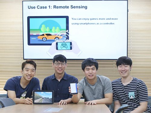 Multi-Device Mobile Platform for App Functionality Sharing
Case 1. Mr. Kim, an employee, logged on to his SNS account using a tablet PC at the airport while traveling overseas. However, a malicious virus was installed on the tablet PC and some photos posted on his SNS were deleted by someone else.
Case 2. Mr. and Mrs. Brown are busy contacting credit card and game companies, because his son, who likes games, purchased a million dollars worth of game items using his smartphone.
Case 3. Mr. Park, who enjoys games, bought a sensor-based racing game through his tablet PC. However, he could not enjoy the racing game on his tablet because it was not comfortable to tilt the device for game control.
The above cases are some of the various problems that can arise in modern society where diverse smart devices, including smartphones, exist. Recently, new technology has been developed to easily solve these problems. Professor Insik Shin from the School of Computing has developed ‘Mobile Plus,’ which is a mobile platform that can share the functionalities of applications between smart devices.
This is a novel technology that allows applications to easily share their functionalities without needing any modifications. Smartphone users often use Facebook to log in to another SNS account like Instagram, or use a gallery app to post some photos on their SNS. These examples are possible, because the applications share their login and photo management functionalities.
The functionality sharing enables users to utilize smartphones in various and convenient ways and allows app developers to easily create applications. However, current mobile platforms such as Android or iOS only support functionality sharing within a single mobile device. It is burdensome for both developers and users to share functionalities across devices because developers would need to create more complex applications and users would need to install the applications on each device.
To address this problem, Professor Shin’s research team developed platform technology to support functionality sharing between devices. The main concept is using virtualization to give the illusion that the applications running on separate devices are on a single device. They succeeded in this virtualization by extending a RPC (Remote Procedure Call) scheme to multi-device environments.
This virtualization technology enables the existing applications to share their functionalities without needing any modifications, regardless of the type of applications. So users can now use them without additional purchases or updates. Mobile Plus can support hardware functionalities like cameras, microphones, and GPS as well as application functionalities such as logins, payments, and photo sharing. Its greatest advantage is its wide range of possible applications.
Professor Shin said, "Mobile Plus is expected to have great synergy with smart home and smart car technologies. It can provide novel user experiences (UXs) so that users can easily utilize various applications of smart home/vehicle infotainment systems by using a smartphone as their hub."
This research was published at ACM MobiSys, an international conference on mobile computing that was hosted in the United States on June 21.
Figure1. Users can securely log on to SNS accounts by using their personal devices
Figure 2. Parents can control impulse shopping of their children.
Figure 3. Users can enjoy games more and more by using the smartphone as a controller.
2017.08.09 View 10765
Multi-Device Mobile Platform for App Functionality Sharing
Case 1. Mr. Kim, an employee, logged on to his SNS account using a tablet PC at the airport while traveling overseas. However, a malicious virus was installed on the tablet PC and some photos posted on his SNS were deleted by someone else.
Case 2. Mr. and Mrs. Brown are busy contacting credit card and game companies, because his son, who likes games, purchased a million dollars worth of game items using his smartphone.
Case 3. Mr. Park, who enjoys games, bought a sensor-based racing game through his tablet PC. However, he could not enjoy the racing game on his tablet because it was not comfortable to tilt the device for game control.
The above cases are some of the various problems that can arise in modern society where diverse smart devices, including smartphones, exist. Recently, new technology has been developed to easily solve these problems. Professor Insik Shin from the School of Computing has developed ‘Mobile Plus,’ which is a mobile platform that can share the functionalities of applications between smart devices.
This is a novel technology that allows applications to easily share their functionalities without needing any modifications. Smartphone users often use Facebook to log in to another SNS account like Instagram, or use a gallery app to post some photos on their SNS. These examples are possible, because the applications share their login and photo management functionalities.
The functionality sharing enables users to utilize smartphones in various and convenient ways and allows app developers to easily create applications. However, current mobile platforms such as Android or iOS only support functionality sharing within a single mobile device. It is burdensome for both developers and users to share functionalities across devices because developers would need to create more complex applications and users would need to install the applications on each device.
To address this problem, Professor Shin’s research team developed platform technology to support functionality sharing between devices. The main concept is using virtualization to give the illusion that the applications running on separate devices are on a single device. They succeeded in this virtualization by extending a RPC (Remote Procedure Call) scheme to multi-device environments.
This virtualization technology enables the existing applications to share their functionalities without needing any modifications, regardless of the type of applications. So users can now use them without additional purchases or updates. Mobile Plus can support hardware functionalities like cameras, microphones, and GPS as well as application functionalities such as logins, payments, and photo sharing. Its greatest advantage is its wide range of possible applications.
Professor Shin said, "Mobile Plus is expected to have great synergy with smart home and smart car technologies. It can provide novel user experiences (UXs) so that users can easily utilize various applications of smart home/vehicle infotainment systems by using a smartphone as their hub."
This research was published at ACM MobiSys, an international conference on mobile computing that was hosted in the United States on June 21.
Figure1. Users can securely log on to SNS accounts by using their personal devices
Figure 2. Parents can control impulse shopping of their children.
Figure 3. Users can enjoy games more and more by using the smartphone as a controller.
2017.08.09 View 10765 -
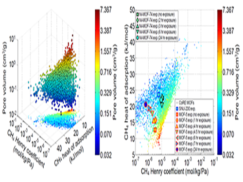 Analysis of Gas Adsorption Properties for Amorphous Porous Materials
Professor Jihan Kim from the Department of Chemical and Biomolecular Engineering at KAIST has developed a method to predict gas adsorption properties of amorphous porous materials.
Metal-organic frameworks (MOFs) have large surface area and high density of pores, making them appropriate for various energy and environmental-related applications. And although most MOFs are crystalline, these structures can deform during synthesis and/or industrial processes, leading to loss in long-range order. Unfortunately, without the structural information, existing computer simulation techniques cannot be used to model these materials.
In this research, Professor Kim’s research team demonstrated that one can replace the material properties of structurally deformed MOFs with those of crystalline MOFs to indirectly analyze/model the material properties of amorphous materials. First, the team conducted simulations on methane gas adsorption properties for over 12,000 crystalline MOFs to obtain a large training set data, and created a resulting structure-property map. Upon mapping the experimental data of amorphous MOFs onto the structure-property map, results showed that regardless of crystallinity, the gas adsorption properties of MOFs showed congruence and consistency amongst one another.
Based on these findings, selected crystalline MOFs with the most similar gas adsorption properties as the collapsed structure from the 12,000 candidates. Then, the team verified that the adsorption properties of these similar MOFs can be successfully transferred to the deformed MOFs across different temperatures and even to different gas molecules (e.g. hydrogen), demonstrating transferability of properties.
These findings allow material property prediction in porous materials such as MOFs without structural information, and the techniques here can be used to better predict and understand optimal materials for various applications including, carbon dioxide capture, gas storage and separations.
This research was conducted in collaboration with Professor Dae-Woon Lim at Kyoto University, Professor Myunghyun Paik at Seoul National University, Professor Minyoung Yoon at Gachon University, and Aadesh Harale at Saudi Arabian Oil Company. The research was published in the Proceedings of the National Academy of Sciences (PNAS) online on 10 July and the co-first authors were Ph. D. candidate WooSeok Jeong and Professor Dae-Woon Lim.
This research was funded by the Saudi Aramco-KAIST CO2 Management Center.
(Figure 1. Trends in structure - material property map and in collapsed structures)
(Figure 2. Transferability between the experimental results of collapsed MOFs and the simulation results of crystalline MOFs)
2017.07.26 View 10540
Analysis of Gas Adsorption Properties for Amorphous Porous Materials
Professor Jihan Kim from the Department of Chemical and Biomolecular Engineering at KAIST has developed a method to predict gas adsorption properties of amorphous porous materials.
Metal-organic frameworks (MOFs) have large surface area and high density of pores, making them appropriate for various energy and environmental-related applications. And although most MOFs are crystalline, these structures can deform during synthesis and/or industrial processes, leading to loss in long-range order. Unfortunately, without the structural information, existing computer simulation techniques cannot be used to model these materials.
In this research, Professor Kim’s research team demonstrated that one can replace the material properties of structurally deformed MOFs with those of crystalline MOFs to indirectly analyze/model the material properties of amorphous materials. First, the team conducted simulations on methane gas adsorption properties for over 12,000 crystalline MOFs to obtain a large training set data, and created a resulting structure-property map. Upon mapping the experimental data of amorphous MOFs onto the structure-property map, results showed that regardless of crystallinity, the gas adsorption properties of MOFs showed congruence and consistency amongst one another.
Based on these findings, selected crystalline MOFs with the most similar gas adsorption properties as the collapsed structure from the 12,000 candidates. Then, the team verified that the adsorption properties of these similar MOFs can be successfully transferred to the deformed MOFs across different temperatures and even to different gas molecules (e.g. hydrogen), demonstrating transferability of properties.
These findings allow material property prediction in porous materials such as MOFs without structural information, and the techniques here can be used to better predict and understand optimal materials for various applications including, carbon dioxide capture, gas storage and separations.
This research was conducted in collaboration with Professor Dae-Woon Lim at Kyoto University, Professor Myunghyun Paik at Seoul National University, Professor Minyoung Yoon at Gachon University, and Aadesh Harale at Saudi Arabian Oil Company. The research was published in the Proceedings of the National Academy of Sciences (PNAS) online on 10 July and the co-first authors were Ph. D. candidate WooSeok Jeong and Professor Dae-Woon Lim.
This research was funded by the Saudi Aramco-KAIST CO2 Management Center.
(Figure 1. Trends in structure - material property map and in collapsed structures)
(Figure 2. Transferability between the experimental results of collapsed MOFs and the simulation results of crystalline MOFs)
2017.07.26 View 10540 -
 Innovative Nanosensor for Disease Diagnosis
(Figure 1. Sensing Device)
(Figure 2. Protein templating route)
Breath pattern recognition is a futuristic diagnostic platform. Simple characterizing target gas concentrations of human exhaled breath will lead to diagnose of the disease as well as physical condition.
A research group under Prof. Il-Doo Kim in the Department of Materials Science has developed diagnostic sensors using protein-encapsulated nanocatalysts, which can diagnose certain diseases by analyzing human exhaled breath. This technology enables early monitoring of various diseases through pattern recognition of biomarker gases related to diseases in human exhalation.
The protein-templated catalyst synthesis route is very simple and versatile for producing not only a single component of catalytic nanoparticles, but also diverse heterogeneous intermetallic catalysts with sizes less than 3 nm. The research team has developed ever more sensitive and selective chemiresistive sensors that can potentially diagnose specific diseases by analyzing exhaled breath gases.
The results of this study, which were contributed by Dr. Sang-Joon Kim and Dr. Seon-Jin Choi as first authors were selected as the cover-featured article in the July issue of 'Accounts of Chemical Research,' an international journal of the American Chemical Society.
In human breath, diverse components are found including water vapor, hydrogen, acetone, toluene, ammonia, hydrogen sulfide, and carbon monoxide, which are more excessively exhaled from patients. Some of these components are closely related to diseases such as asthma, lung cancer, type 1 diabetes mellitus, and halitosis.
Breath analysis for disease diagnosis started from capturing exhaled breaths in a Tedlar bag and subsequently the captured breath gases were injected into a miniaturized sensor system, similar to an alcohol detector. It is possible to analyze exhaled breath very rapidly with a simple analyzing process. The breath analysis can detect trace changes in exhaled breath components, which contribute to early diagnosis of diseases.
However, technological advances are needed to accurately analyze gases in the breath, which occur at very low levels, from 1 ppb to 1 ppm. In particular, it has been a critical challenge for chemiresistive type chemical sensors to selectively detect specific biomarkers in thousands of interfering gases including humid vapor.
Conventionally, noble metallic catalysts such as platinum and palladium have been functionalized onto metal oxide sensing layers. However, the gas sensitivity was not enough to detect ppb-levels of biomarker species in exhaled breath.
To overcome the current limitations, the research team utilized nanoscale protein (apoferritin) in animals as sacrificial templates. The protein templates possess hollow nanocages at the core site and various alloy catalytic nanoparticles can be encapsulated inside the protein nanocages.
The protein nanocages are advantageous because a nearly unlimited number of material compositions in the periodic table can be assembled for the synthesis of heterogeneous catalytic nanoparticles. In addition, intermetallic nanocatalysts with a controlled atomic ratio of two different elements can be achieved using the protein nanocages, which is an innovative strategy for finding new types of catalysts. For example, highly efficient platinum-based catalysts can be synthesized, such as platinum-palladium (PtPd), platinum-nickel (PtNi), platinum-ruthenium (PtRu), and platinum-yttrium (PtY).
The research team developed outstanding sensing layers consisting of metal oxide nanofibers functionalized by the heterogeneous catalysts with large and highly-porous surface areas, which are especially optimized for selective detection of specific biomarkers. The biomarker sensing performance was improved approximately 3~4-fold as compared to the conventional single component of platinum and palladium catalysts-loaded nanofiber sensors. In particular, 100-fold resistance transitions toward acetone (1 ppm) and hydrogen sulfide (1 ppm) were observed in exhaled breath sensors using the heterogeneous nanocatalysts, which is the best performance ever reported in literature.
The research team developed a disease diagnosis platform that recognizes individual breathing patterns by using a multiple sensor array system with diverse sensing layers and heterogeneous catalysts, so that the people can easily identify health abnormalities. Using a 16-sensor array system, physical conditions can be continuously monitored by analyzing concentration changes of biomarkers in exhaled breath gases.
Prof. Kim said, “New types of heterogeneous nanocatalysts were synthesized using protein templates with sizes around 2 nm and functionalized on various metal oxide nanofiber sensing layers. The established sensing libraries can detect biomarker species with high sensitivity and selectivity.” He added, “the new and innovative breath gas analysis platform will be very helpful for reducing medical expenditures and continuous monitoring of physical conditions”
Patents related to this technology were licensed to two companies in March and June this year.
2017.07.19 View 11431
Innovative Nanosensor for Disease Diagnosis
(Figure 1. Sensing Device)
(Figure 2. Protein templating route)
Breath pattern recognition is a futuristic diagnostic platform. Simple characterizing target gas concentrations of human exhaled breath will lead to diagnose of the disease as well as physical condition.
A research group under Prof. Il-Doo Kim in the Department of Materials Science has developed diagnostic sensors using protein-encapsulated nanocatalysts, which can diagnose certain diseases by analyzing human exhaled breath. This technology enables early monitoring of various diseases through pattern recognition of biomarker gases related to diseases in human exhalation.
The protein-templated catalyst synthesis route is very simple and versatile for producing not only a single component of catalytic nanoparticles, but also diverse heterogeneous intermetallic catalysts with sizes less than 3 nm. The research team has developed ever more sensitive and selective chemiresistive sensors that can potentially diagnose specific diseases by analyzing exhaled breath gases.
The results of this study, which were contributed by Dr. Sang-Joon Kim and Dr. Seon-Jin Choi as first authors were selected as the cover-featured article in the July issue of 'Accounts of Chemical Research,' an international journal of the American Chemical Society.
In human breath, diverse components are found including water vapor, hydrogen, acetone, toluene, ammonia, hydrogen sulfide, and carbon monoxide, which are more excessively exhaled from patients. Some of these components are closely related to diseases such as asthma, lung cancer, type 1 diabetes mellitus, and halitosis.
Breath analysis for disease diagnosis started from capturing exhaled breaths in a Tedlar bag and subsequently the captured breath gases were injected into a miniaturized sensor system, similar to an alcohol detector. It is possible to analyze exhaled breath very rapidly with a simple analyzing process. The breath analysis can detect trace changes in exhaled breath components, which contribute to early diagnosis of diseases.
However, technological advances are needed to accurately analyze gases in the breath, which occur at very low levels, from 1 ppb to 1 ppm. In particular, it has been a critical challenge for chemiresistive type chemical sensors to selectively detect specific biomarkers in thousands of interfering gases including humid vapor.
Conventionally, noble metallic catalysts such as platinum and palladium have been functionalized onto metal oxide sensing layers. However, the gas sensitivity was not enough to detect ppb-levels of biomarker species in exhaled breath.
To overcome the current limitations, the research team utilized nanoscale protein (apoferritin) in animals as sacrificial templates. The protein templates possess hollow nanocages at the core site and various alloy catalytic nanoparticles can be encapsulated inside the protein nanocages.
The protein nanocages are advantageous because a nearly unlimited number of material compositions in the periodic table can be assembled for the synthesis of heterogeneous catalytic nanoparticles. In addition, intermetallic nanocatalysts with a controlled atomic ratio of two different elements can be achieved using the protein nanocages, which is an innovative strategy for finding new types of catalysts. For example, highly efficient platinum-based catalysts can be synthesized, such as platinum-palladium (PtPd), platinum-nickel (PtNi), platinum-ruthenium (PtRu), and platinum-yttrium (PtY).
The research team developed outstanding sensing layers consisting of metal oxide nanofibers functionalized by the heterogeneous catalysts with large and highly-porous surface areas, which are especially optimized for selective detection of specific biomarkers. The biomarker sensing performance was improved approximately 3~4-fold as compared to the conventional single component of platinum and palladium catalysts-loaded nanofiber sensors. In particular, 100-fold resistance transitions toward acetone (1 ppm) and hydrogen sulfide (1 ppm) were observed in exhaled breath sensors using the heterogeneous nanocatalysts, which is the best performance ever reported in literature.
The research team developed a disease diagnosis platform that recognizes individual breathing patterns by using a multiple sensor array system with diverse sensing layers and heterogeneous catalysts, so that the people can easily identify health abnormalities. Using a 16-sensor array system, physical conditions can be continuously monitored by analyzing concentration changes of biomarkers in exhaled breath gases.
Prof. Kim said, “New types of heterogeneous nanocatalysts were synthesized using protein templates with sizes around 2 nm and functionalized on various metal oxide nanofiber sensing layers. The established sensing libraries can detect biomarker species with high sensitivity and selectivity.” He added, “the new and innovative breath gas analysis platform will be very helpful for reducing medical expenditures and continuous monitoring of physical conditions”
Patents related to this technology were licensed to two companies in March and June this year.
2017.07.19 View 11431 -
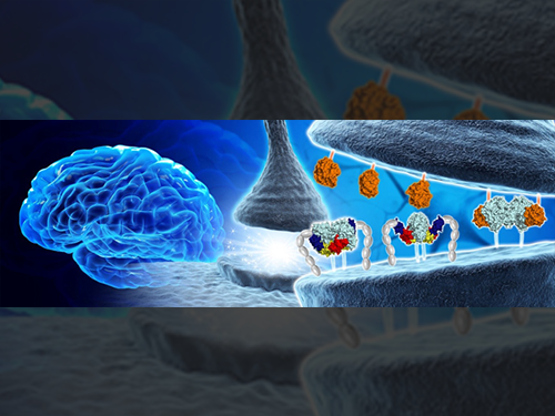 Structural Insights into the Modulation of Synaptic Adhesion by MDGA for Synaptogenesis
Synapses connected by various synaptic adhesion molecules are communication spaces between neurons for transmitting information. Among various synaptic adhesion molecules, neuroligins are arguably the most widely studied class of postsynaptic adhesion molecules, which mainly interact with presynaptic neurexins to induce excitatory or inhibitory synapse development. Recently, the membrane-associated mucin (MAM) domain-containing GPI anchor protein 1 (MDGA1) has been characterized as a key suppressor of Neuroligin-2/Neurexin-1β-mediated inhibitory synapse development, but how it acts remains a mystery.
In a recent issue of Neuron, published on June 21, 2017, a research team led by Professor Ho Min Kim at the Graduate School of Medical Science and Engineering of KAIST reported the three-dimensional structure of MDGA1/Neuroligin-2 complex and mechanistic insights into how MDGAs negatively modulate synapse development governed by Neurexins/Neuroligins trans -synaptic adhesion complex.
MDGA1 consists of six Ig-like domains, fibronectin type III repeat domain, and MAM domain . The crystal structure of MDGA1/Neuroligin-2 complex reveals that they form the 2:2 hetero-tetrameric complex and only the Ig1-Ig2 domains of MDGA1 are involved in interactions with Neuroligin-2. The structural comparison between the MDGA1/Neuroligin-2 and Neurexin-1β/Neuroligin-1 complexes intriguingly indicates that the Neuroligin-2 region binding to MDGA1 largely overlaps with that of Neurexin-1β, but the interaction interface of the MDGA1/Neuroligin-2 complex is much larger than that of the Neurexin-1β/Neuroligin-1 complex. This explains why Neuroligin-2 binds stronger to MDGA1 than Neurexin-1β, and how the favored MDGA1 binding to Neuroligin-2 sterically blocks the interaction between Neuroligin-2 and Neurexin-1β, which is critical for the suppression of inhibitory synapse development.
“Although we found that MDGA Ig domains (Ig 1 and Ig 2) are sufficient to form a complex with NL2, other extracellular domains, including Ig 3–6, FN III, and MAM domains, may also contribute to stable cis-interactions between MDGA1 and Neuroligin-2 by providing conformational flexibility. Therefore, further structural analysis of full-length MDGA will be required,” Professor Kim said.
Neuroligin-2 specifically promotes the development of inhibitory synapses, whereas neuroligin-1 promotes the development of excitatory synapses. Recently, not only MDGA1, but also MDGA2 have emerged as synaptic regulators for the development of excitatory or inhibitory synapses. In vitro biochemical analysis in this research clearly demonstrates that Neuroligin-1 and Neuroligin-2 bind to both MDGA1 and MDGA2 with comparable affinity. However, pull-down assays using detergent-solubilized mouse brain membrane fractions show the specific interaction of MDGA1 with Neuroligin-2, but not with Neuroligin-1. “This suggests that unidentified processes may dictate the selective association of MDGA1 with Neuroligin-2 in vivo , ” explained Professor Jaewon Ko at the Daegu Gyeongbuk Institute of Science and Technology (DGIST).
A balance between excitatory and inhibitory synapses is crucial to healthy cognition and behavior. Mutations in neuroligins, neurexins, and MDGAs, which can disrupt the excitatory/inhibitory balance, are associated with neuropsychiatric diseases such as autism and schizophrenia. Jung A Kim at KAIST, first author in this study, said, “Our discovery from integrative investigations are an important first step both for a better understanding of Neuroligin/Neurexin synaptic adhesion pathways and MDGA-mediated regulation of synapse development as well as the development of potential new therapies for autism, schizophrenia, and epilepsy.”
2017.07.10 View 9644
Structural Insights into the Modulation of Synaptic Adhesion by MDGA for Synaptogenesis
Synapses connected by various synaptic adhesion molecules are communication spaces between neurons for transmitting information. Among various synaptic adhesion molecules, neuroligins are arguably the most widely studied class of postsynaptic adhesion molecules, which mainly interact with presynaptic neurexins to induce excitatory or inhibitory synapse development. Recently, the membrane-associated mucin (MAM) domain-containing GPI anchor protein 1 (MDGA1) has been characterized as a key suppressor of Neuroligin-2/Neurexin-1β-mediated inhibitory synapse development, but how it acts remains a mystery.
In a recent issue of Neuron, published on June 21, 2017, a research team led by Professor Ho Min Kim at the Graduate School of Medical Science and Engineering of KAIST reported the three-dimensional structure of MDGA1/Neuroligin-2 complex and mechanistic insights into how MDGAs negatively modulate synapse development governed by Neurexins/Neuroligins trans -synaptic adhesion complex.
MDGA1 consists of six Ig-like domains, fibronectin type III repeat domain, and MAM domain . The crystal structure of MDGA1/Neuroligin-2 complex reveals that they form the 2:2 hetero-tetrameric complex and only the Ig1-Ig2 domains of MDGA1 are involved in interactions with Neuroligin-2. The structural comparison between the MDGA1/Neuroligin-2 and Neurexin-1β/Neuroligin-1 complexes intriguingly indicates that the Neuroligin-2 region binding to MDGA1 largely overlaps with that of Neurexin-1β, but the interaction interface of the MDGA1/Neuroligin-2 complex is much larger than that of the Neurexin-1β/Neuroligin-1 complex. This explains why Neuroligin-2 binds stronger to MDGA1 than Neurexin-1β, and how the favored MDGA1 binding to Neuroligin-2 sterically blocks the interaction between Neuroligin-2 and Neurexin-1β, which is critical for the suppression of inhibitory synapse development.
“Although we found that MDGA Ig domains (Ig 1 and Ig 2) are sufficient to form a complex with NL2, other extracellular domains, including Ig 3–6, FN III, and MAM domains, may also contribute to stable cis-interactions between MDGA1 and Neuroligin-2 by providing conformational flexibility. Therefore, further structural analysis of full-length MDGA will be required,” Professor Kim said.
Neuroligin-2 specifically promotes the development of inhibitory synapses, whereas neuroligin-1 promotes the development of excitatory synapses. Recently, not only MDGA1, but also MDGA2 have emerged as synaptic regulators for the development of excitatory or inhibitory synapses. In vitro biochemical analysis in this research clearly demonstrates that Neuroligin-1 and Neuroligin-2 bind to both MDGA1 and MDGA2 with comparable affinity. However, pull-down assays using detergent-solubilized mouse brain membrane fractions show the specific interaction of MDGA1 with Neuroligin-2, but not with Neuroligin-1. “This suggests that unidentified processes may dictate the selective association of MDGA1 with Neuroligin-2 in vivo , ” explained Professor Jaewon Ko at the Daegu Gyeongbuk Institute of Science and Technology (DGIST).
A balance between excitatory and inhibitory synapses is crucial to healthy cognition and behavior. Mutations in neuroligins, neurexins, and MDGAs, which can disrupt the excitatory/inhibitory balance, are associated with neuropsychiatric diseases such as autism and schizophrenia. Jung A Kim at KAIST, first author in this study, said, “Our discovery from integrative investigations are an important first step both for a better understanding of Neuroligin/Neurexin synaptic adhesion pathways and MDGA-mediated regulation of synapse development as well as the development of potential new therapies for autism, schizophrenia, and epilepsy.”
2017.07.10 View 9644 -
 Cooperative Tumor Cell Membrane-Targeted Phototherapy
A KAIST research team led by Professor Ji-Ho Park in the Bio and Brain Engineering Department at KAIST developed a technology for the effective treatment of cancer by delivering synthetic receptors throughout tumor tissue. The study, led by Ph.D. candidate Heegon Kim, was published online in Nature Communications on June 19.
Cancer targeted therapy generally refers to therapy targeting specific molecules that are involved in the growth and generation of cancer. The targeted delivery of therapeutics using targeting agents such as antibodies or nanomaterials has improved the precision and safety of cancer therapy.
However, the paucity and heterogeneity of identified molecular targets within tumors have resulted in poor and uneven distribution of targeted agents, thus compromising treatment outcomes.
To solve this problem, the team constructed a cooperative targeting system in which synthetic and biological nanocomponents participate together in the tumor cell membrane-selective localization of synthetic receptors to amplify the subsequent targeting of therapeutics. Here, synthetic and biological nanocomponents refer to liposomes and extracellular vesicles, respectively.
The synthetic receptors are first delivered selectively to tumor cell membranes in the perivascular region using liposomes. By hitchhiking with extracellular vesicles secreted by the cells, the synthetic receptors are transferred to neighboring cells and further spread throughout the tumor tissues where the molecular targets are limited.
Hitchhiking extracellular vesicles for delivery of synthetic receptors was possible since extracellular vesicles, such as exosomes, mediate intercellular communications by transferring various biological components such as lipids, cytosolic proteins, and RNA through a membrane fusion process. They also play a supportive role in promoting tumor progression in that tumor-derived extracellular vesicles deliver oncogenic signals to normal host cells.
The team showed that this tumor cell membrane-targeted delivery of synthetic receptors led to a uniform distribution of synthetic receptors throughout a tumor and subsequently led to enhanced phototherapeutic efficacy of the targeted photosensitizer.
Professor Park said, “The cooperative tumor targeting system is expected to be applied in treating various diseases that are hard to target.”
The research was funded by the Basic Science Research Program through the National Research Foundation funded by the Ministry of Science, ICT & Future Planning, and the National R&D Program for Cancer Control funded by the Ministry for Health and Welfare.
(Ph.D. candidates Hee Gon Kim (left) and Chanhee Oh)
Figure 1. A schematic of a cooperative tumor targeting system via delivery of synthetic receptors.
Figure 2. A confocal microscopic image of a tumor section after cooperative targeting by synthetic receptor delivery. Green and magenta represent vessels and therapeutic agents inside a tumor respectively.
2017.07.07 View 11990
Cooperative Tumor Cell Membrane-Targeted Phototherapy
A KAIST research team led by Professor Ji-Ho Park in the Bio and Brain Engineering Department at KAIST developed a technology for the effective treatment of cancer by delivering synthetic receptors throughout tumor tissue. The study, led by Ph.D. candidate Heegon Kim, was published online in Nature Communications on June 19.
Cancer targeted therapy generally refers to therapy targeting specific molecules that are involved in the growth and generation of cancer. The targeted delivery of therapeutics using targeting agents such as antibodies or nanomaterials has improved the precision and safety of cancer therapy.
However, the paucity and heterogeneity of identified molecular targets within tumors have resulted in poor and uneven distribution of targeted agents, thus compromising treatment outcomes.
To solve this problem, the team constructed a cooperative targeting system in which synthetic and biological nanocomponents participate together in the tumor cell membrane-selective localization of synthetic receptors to amplify the subsequent targeting of therapeutics. Here, synthetic and biological nanocomponents refer to liposomes and extracellular vesicles, respectively.
The synthetic receptors are first delivered selectively to tumor cell membranes in the perivascular region using liposomes. By hitchhiking with extracellular vesicles secreted by the cells, the synthetic receptors are transferred to neighboring cells and further spread throughout the tumor tissues where the molecular targets are limited.
Hitchhiking extracellular vesicles for delivery of synthetic receptors was possible since extracellular vesicles, such as exosomes, mediate intercellular communications by transferring various biological components such as lipids, cytosolic proteins, and RNA through a membrane fusion process. They also play a supportive role in promoting tumor progression in that tumor-derived extracellular vesicles deliver oncogenic signals to normal host cells.
The team showed that this tumor cell membrane-targeted delivery of synthetic receptors led to a uniform distribution of synthetic receptors throughout a tumor and subsequently led to enhanced phototherapeutic efficacy of the targeted photosensitizer.
Professor Park said, “The cooperative tumor targeting system is expected to be applied in treating various diseases that are hard to target.”
The research was funded by the Basic Science Research Program through the National Research Foundation funded by the Ministry of Science, ICT & Future Planning, and the National R&D Program for Cancer Control funded by the Ministry for Health and Welfare.
(Ph.D. candidates Hee Gon Kim (left) and Chanhee Oh)
Figure 1. A schematic of a cooperative tumor targeting system via delivery of synthetic receptors.
Figure 2. A confocal microscopic image of a tumor section after cooperative targeting by synthetic receptor delivery. Green and magenta represent vessels and therapeutic agents inside a tumor respectively.
2017.07.07 View 11990 -
 Top 10 Emerging Technologies of 2017
The World Economic Forum’s Expert Network and Global Future Councils in collaboration with Scientific American and its Board of Advisors announced the top 10 emerging technologies of 2017 on June 26 in Dalian, China where the 2017 Summer Davos Forum is being held. Each technology was chosen for its potential to improve lives, transform industries, and safeguard the planet.
The KAIST delegation, headed by President Sung-Chul Shin, is participating in the forum’s diverse activities including IdeasLab and GULF (Global University Leaders Forum). KAIST is the only Korean representative participating in the IdeasLab. KAIST Distinguished Professor Sang Yup Lee of the Department of Chemical and Biomolecular Engineering, director of KAIST Institute, has served as a committee member of the Global Agenda Council on Emerging Technologies since 2012 and Global Future Council on the Fourth Industrial Revolution. He also chairs the Global Future Council on Biotechnologies.
Professor Lee said, “Very diverse technological breakthroughs were proposed for the final list of candidates. We made the final selections through very in-depth discussion with experts in each field.
We focused on the technologies which have a level of maturity that will enable them to be adopted widely within three to five years."
The top 10 emerging technologies are
(courtesy from https://
www.weforum.org/agenda/2017/06/these-are-the-top-10-emerging-technologies-of-2017):
2017 10대 기술.
1. Liquid biopsies
Liquid biopsies mark a step forward in the fight against cancer. First, they are an alternative where traditional tissue-based biopsies are not possible. Second, they provide a full spectrum of information compared to tissue samples, which only reflect the information available in the sample. Lastly, by homing in on circulating-tumor DNA (ctDNA), genetic material that routinely finds its way from cancer cells into the bloodstream, disease progression or resistance to treatment can be spotted much faster than otherwise relying on symptoms or imaging.
2. Harvesting clean water from air
The ability to extract clean water from air is not new, however existing techniques require high moisture levels and a lot of electricity. This is changing. A team from MIT and University of California, Berkeley has successfully tested a process using porous crystals that convert the water using no energy at all.
3. Deep learning for visual tasks
Computers are beginning to recognize images better than humans. Thanks to deep learning, an emerging field of artificial intelligence, computer-vision technologies are increasingly being used in applications as diverse as driving autonomous vehicles, medical diagnostics, damage assessment for insurance claims, and monitoring water levels and crop yield.
4. Liquid fuels from sunshine
Can we mimic the humble leaf to create artificial photosynthesis to generate and store energy? The prospects are looking increasingly positive. The answer lies in using sunlight-activated catalysts to split water molecules into water and hydrogen, and then using the same hydrogen to convert CO2 into hydrocarbons.
5. The Human Cell Atlas
An international collaboration aimed at deciphering the human body, called the Human Cell Atlas, was launched in October 2016. The project aims to identify every cell type in every tissue; learn exactly which genes, proteins, and other molecules are active in each type, and the processes which control that activity.
6. Precision farming
The Fourth Industrial Revolution is providing farmers with a new set of tools to boost crop yield and quality while reducing water and chemical use. Sensors, robots, GPS, mapping tools, and data-analytics software are all being used to customize the care that plants need.
7. Affordable catalysts for green vehicles
Progress is being made on a promising zero-emission technology, the hydrogen-fed fuel cell. Progress to date has been stymied by the high price of catalysts which contain platinum. However, much progress has been made in reducing reliance on this rare and expensive metal, and the latest developments involve catalysts that include no platinum, or in some cases no metal at all.
8. Genomic vaccines
Vaccines based on genes are superior to more conventional ones in a number of ways. They are faster to manufacture, which is crucial during violent outbreaks. Compared to manufacturing proteins in cell cultures or eggs, producing genetic material should also be simpler and less expensive.
9. Sustainable design of communities
Applying green construction to multiple buildings at once has the potential to revolutionize the amount of energy and water we consume. Sending locally-generated solar power to a smart microgrid could reduce electricity consumption by half and reduce carbon emissions to zero if a project currently under development at the University of California at Berkeley goes according to plan.
10. Quantum computing
Quantum computers’ almost limitless potential has only ever been matched by the difficulty and cost of their construction. This explains why today the small ones that have been built have not yet managed to exceed the power of supercomputers. But progress is being made and in 2016 the technology firm IBM provided public access to the first quantum computer in the cloud.
2017.06.28 View 13930
Top 10 Emerging Technologies of 2017
The World Economic Forum’s Expert Network and Global Future Councils in collaboration with Scientific American and its Board of Advisors announced the top 10 emerging technologies of 2017 on June 26 in Dalian, China where the 2017 Summer Davos Forum is being held. Each technology was chosen for its potential to improve lives, transform industries, and safeguard the planet.
The KAIST delegation, headed by President Sung-Chul Shin, is participating in the forum’s diverse activities including IdeasLab and GULF (Global University Leaders Forum). KAIST is the only Korean representative participating in the IdeasLab. KAIST Distinguished Professor Sang Yup Lee of the Department of Chemical and Biomolecular Engineering, director of KAIST Institute, has served as a committee member of the Global Agenda Council on Emerging Technologies since 2012 and Global Future Council on the Fourth Industrial Revolution. He also chairs the Global Future Council on Biotechnologies.
Professor Lee said, “Very diverse technological breakthroughs were proposed for the final list of candidates. We made the final selections through very in-depth discussion with experts in each field.
We focused on the technologies which have a level of maturity that will enable them to be adopted widely within three to five years."
The top 10 emerging technologies are
(courtesy from https://
www.weforum.org/agenda/2017/06/these-are-the-top-10-emerging-technologies-of-2017):
2017 10대 기술.
1. Liquid biopsies
Liquid biopsies mark a step forward in the fight against cancer. First, they are an alternative where traditional tissue-based biopsies are not possible. Second, they provide a full spectrum of information compared to tissue samples, which only reflect the information available in the sample. Lastly, by homing in on circulating-tumor DNA (ctDNA), genetic material that routinely finds its way from cancer cells into the bloodstream, disease progression or resistance to treatment can be spotted much faster than otherwise relying on symptoms or imaging.
2. Harvesting clean water from air
The ability to extract clean water from air is not new, however existing techniques require high moisture levels and a lot of electricity. This is changing. A team from MIT and University of California, Berkeley has successfully tested a process using porous crystals that convert the water using no energy at all.
3. Deep learning for visual tasks
Computers are beginning to recognize images better than humans. Thanks to deep learning, an emerging field of artificial intelligence, computer-vision technologies are increasingly being used in applications as diverse as driving autonomous vehicles, medical diagnostics, damage assessment for insurance claims, and monitoring water levels and crop yield.
4. Liquid fuels from sunshine
Can we mimic the humble leaf to create artificial photosynthesis to generate and store energy? The prospects are looking increasingly positive. The answer lies in using sunlight-activated catalysts to split water molecules into water and hydrogen, and then using the same hydrogen to convert CO2 into hydrocarbons.
5. The Human Cell Atlas
An international collaboration aimed at deciphering the human body, called the Human Cell Atlas, was launched in October 2016. The project aims to identify every cell type in every tissue; learn exactly which genes, proteins, and other molecules are active in each type, and the processes which control that activity.
6. Precision farming
The Fourth Industrial Revolution is providing farmers with a new set of tools to boost crop yield and quality while reducing water and chemical use. Sensors, robots, GPS, mapping tools, and data-analytics software are all being used to customize the care that plants need.
7. Affordable catalysts for green vehicles
Progress is being made on a promising zero-emission technology, the hydrogen-fed fuel cell. Progress to date has been stymied by the high price of catalysts which contain platinum. However, much progress has been made in reducing reliance on this rare and expensive metal, and the latest developments involve catalysts that include no platinum, or in some cases no metal at all.
8. Genomic vaccines
Vaccines based on genes are superior to more conventional ones in a number of ways. They are faster to manufacture, which is crucial during violent outbreaks. Compared to manufacturing proteins in cell cultures or eggs, producing genetic material should also be simpler and less expensive.
9. Sustainable design of communities
Applying green construction to multiple buildings at once has the potential to revolutionize the amount of energy and water we consume. Sending locally-generated solar power to a smart microgrid could reduce electricity consumption by half and reduce carbon emissions to zero if a project currently under development at the University of California at Berkeley goes according to plan.
10. Quantum computing
Quantum computers’ almost limitless potential has only ever been matched by the difficulty and cost of their construction. This explains why today the small ones that have been built have not yet managed to exceed the power of supercomputers. But progress is being made and in 2016 the technology firm IBM provided public access to the first quantum computer in the cloud.
2017.06.28 View 13930