research
-
 KAIST's Mathematician Reveals the Mechanism for Sustaining Biological Rhythms
Our bodies have a variety of biological clocks that follow rhythms or oscillations with periods ranging from seconds to days. For example, our hearts beat every second, and cells divide periodically. The circadian clock located in the hypothalamus generates twenty-four hour rhythms, timing our sleep and hormone release. How do these biological clocks or circuits generate and sustain the stable rhythms that are essential to life?
Jae Kyoung Kim, who is an assistant professor in the Department of Mathematical Sciences at KAIST, has predicted how these biological circuits generate rhythms and control their robustness, utilizing mathematical modeling based on differential equations and stochastic parameter sampling. Based on his prediction, using synthetic biology, a research team headed by Matthew Bennett of Rice University constructed a novel biological circuit that spans two genetically engineered strains of bacteria, one serves as an activator and the other as a repressor to regulate gene expression across multiple cell types, and found that the circuit generates surprisingly robust rhythms under various conditions.
The results of the research conducted in collaboration with KAIST (Korea Institute of Science and Technology), Rice University, and the University of Houston were published in Science (August 28, 2015 issue). The title of the paper is "Emergent Genetic Oscillations in a Synthetic Microbial Consortium" .
The top-down research approach, which focuses on identifying the components of biological circuits, limits our understanding of the mechanisms in which the circuits generate rhythms. Synthetic biology, a rapidly growing field at the interface of biosciences and engineering, however, uses a bottom-up approach.
Synthetic biologists can create complex circuits out of simpler components, and some of these new genetic circuits are capable of fluctuation to regulate gene production. In the same way that electrical engineers understand how an electrical circuit works as they construct batteries, resistors, and wires, synthetic biologists can understand better about biological circuits if they put them together using genes and proteins. However, due to the complexity of biological systems, both experiments and mathematical modeling need to be applied hand in hand to design these biological circuits and understand their function.
In this research, an interdisciplinary approach proved that a synthetic intercellular singling circuit generates robust rhythms to create a cooperative microbial system. Specifically, Kim's mathematical analysis suggested, and experiments confirmed, that the presence of negative feedback loops in addition to a core transcriptional negative feedback loop can explain the robustness of rhythms in this system. This result provides important clues about the fundamental mechanism of robust rhythm generation in biological systems.
Furthermore, rather than constructing the entire circuit inside a single bacterial strain, the circuit was split among two strains of Escherichia coli bacterium. When the strains were grown together, the bacteria exchanged information, completing the circuit. Thus, this research also shows how, by regulating individual cells within the system, complex biological systems can be controlled, which in turn influences each other (e.g., the gut microbiome in humans).
###
Ye Chen, a graduate student in Bennett's laboratory at Rice University, and Jae Kyoung Kim, an assistant professor at KAIST and a former postdoctoral fellow at Ohio State University, are the lead authors of the paper. The co-authors are Rice graduate student Andrew Hirning and Krešimir Josic?, a professor of mathematics at the University of Houston. Bennett is the Assistant Professor of the Biochemistry and Cell Biology Department at Rice University.
About the researcher: While Jae Kyoung Kim is a mathematician, he has also solved various biological puzzles in collaboration with various experimental laboratories of Matthew Bennett at Rice University, David Virshup at Duke and the National University of Singapore, Carla Finkielstein at Virginia Polytechnic Institute and State University, Choo-Gon Lee at the Florida State University, Seung-Hee Yoo at the Medical School of the University of Texas, Toru Takumi at RIKEN Brain Science Institute, and Travis Wager at Pfizer Inc. He has used non-linear dynamics and stochastic analysis to understand the function of biochemical networks in biological systems. In particular, he is interested in mechanisms generating and regulating biological rhythms.
Picture 1: This schematic image is the design of a biological circuit between two strains of bacteria and the part of differential equations used to understand the function of the biological circuit.
Picture 2: The core transcriptional negative feedback loop and additional negative feedback loop in the biological circuit (picture 1) generate robust rhythms. The snapshots correspond the red dots in the time series graph.
2015.08.31 View 9300
KAIST's Mathematician Reveals the Mechanism for Sustaining Biological Rhythms
Our bodies have a variety of biological clocks that follow rhythms or oscillations with periods ranging from seconds to days. For example, our hearts beat every second, and cells divide periodically. The circadian clock located in the hypothalamus generates twenty-four hour rhythms, timing our sleep and hormone release. How do these biological clocks or circuits generate and sustain the stable rhythms that are essential to life?
Jae Kyoung Kim, who is an assistant professor in the Department of Mathematical Sciences at KAIST, has predicted how these biological circuits generate rhythms and control their robustness, utilizing mathematical modeling based on differential equations and stochastic parameter sampling. Based on his prediction, using synthetic biology, a research team headed by Matthew Bennett of Rice University constructed a novel biological circuit that spans two genetically engineered strains of bacteria, one serves as an activator and the other as a repressor to regulate gene expression across multiple cell types, and found that the circuit generates surprisingly robust rhythms under various conditions.
The results of the research conducted in collaboration with KAIST (Korea Institute of Science and Technology), Rice University, and the University of Houston were published in Science (August 28, 2015 issue). The title of the paper is "Emergent Genetic Oscillations in a Synthetic Microbial Consortium" .
The top-down research approach, which focuses on identifying the components of biological circuits, limits our understanding of the mechanisms in which the circuits generate rhythms. Synthetic biology, a rapidly growing field at the interface of biosciences and engineering, however, uses a bottom-up approach.
Synthetic biologists can create complex circuits out of simpler components, and some of these new genetic circuits are capable of fluctuation to regulate gene production. In the same way that electrical engineers understand how an electrical circuit works as they construct batteries, resistors, and wires, synthetic biologists can understand better about biological circuits if they put them together using genes and proteins. However, due to the complexity of biological systems, both experiments and mathematical modeling need to be applied hand in hand to design these biological circuits and understand their function.
In this research, an interdisciplinary approach proved that a synthetic intercellular singling circuit generates robust rhythms to create a cooperative microbial system. Specifically, Kim's mathematical analysis suggested, and experiments confirmed, that the presence of negative feedback loops in addition to a core transcriptional negative feedback loop can explain the robustness of rhythms in this system. This result provides important clues about the fundamental mechanism of robust rhythm generation in biological systems.
Furthermore, rather than constructing the entire circuit inside a single bacterial strain, the circuit was split among two strains of Escherichia coli bacterium. When the strains were grown together, the bacteria exchanged information, completing the circuit. Thus, this research also shows how, by regulating individual cells within the system, complex biological systems can be controlled, which in turn influences each other (e.g., the gut microbiome in humans).
###
Ye Chen, a graduate student in Bennett's laboratory at Rice University, and Jae Kyoung Kim, an assistant professor at KAIST and a former postdoctoral fellow at Ohio State University, are the lead authors of the paper. The co-authors are Rice graduate student Andrew Hirning and Krešimir Josic?, a professor of mathematics at the University of Houston. Bennett is the Assistant Professor of the Biochemistry and Cell Biology Department at Rice University.
About the researcher: While Jae Kyoung Kim is a mathematician, he has also solved various biological puzzles in collaboration with various experimental laboratories of Matthew Bennett at Rice University, David Virshup at Duke and the National University of Singapore, Carla Finkielstein at Virginia Polytechnic Institute and State University, Choo-Gon Lee at the Florida State University, Seung-Hee Yoo at the Medical School of the University of Texas, Toru Takumi at RIKEN Brain Science Institute, and Travis Wager at Pfizer Inc. He has used non-linear dynamics and stochastic analysis to understand the function of biochemical networks in biological systems. In particular, he is interested in mechanisms generating and regulating biological rhythms.
Picture 1: This schematic image is the design of a biological circuit between two strains of bacteria and the part of differential equations used to understand the function of the biological circuit.
Picture 2: The core transcriptional negative feedback loop and additional negative feedback loop in the biological circuit (picture 1) generate robust rhythms. The snapshots correspond the red dots in the time series graph.
2015.08.31 View 9300 -
 'Engineered Bacterium Produces 1,3-Diaminopropane'
A research team led by Distinguished Professor Sang Yup Lee of the Department of Chemical and Biomolecular Engineering at KAIST reported, for the first time, the production of 1,3-diaminopropane via fermentation of an engineered bacterium.
1,3-Diaminopropane is a three carbon diamine, which has a wide range of industrial applications including epoxy resin and cross-linking agents, as well as precursors for pharmaceuticals, agrochemicals, and organic chemicals. It can also be polymerized with dicarboxylic acids to make polyamides (nylons) for use as engineering plastics, medical materials, and adhesives.
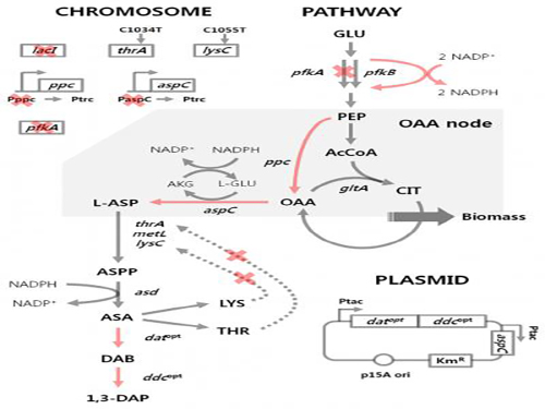
Traditionally, 1,3-diaminopropane is derived from petroleum-based processes. In effort to address critical problems such as the depletion of petroleum and environmental issues inherent to the petroleum-based processes, the research team has developed an Escherichia coli (E. coli) strain capable of producing 1,3-diaminopropane. Using this technology, 1,3-diaminopropane can now be produced from renewable biomass instead of petroleum.
E. coli as found in nature is unable to produce 1,3-diaminopropane. Metabolic engineering, a technology to transform microorganisms into highly efficient microbial cell factories capable of producing chemical compounds of interest, was utilized to engineer the E. coli strain. First, naturally existing metabolic pathways for the biosynthesis of 1,3-diaminopropane were introduced into a virtual cell in silico to determine the most efficient metabolic pathway for the 1,3-diaminopropane production. The metabolic pathway selected was then introduced into an E. coli strain and successfully produced 1,3-diaminopropane for the first time in the world.
The research team applied metabolic engineering additionally, and the production titer of 1,3-diaminopropane increased about 21 fold. The Fed-batch fermentation of the engineered E. coli strain produced 13 grams per liter of 1,3-diaminoproapne. With this technology, 1,3-diaminopropane can be produced using renewable biomass, and it will be the starting point for replacing the current petroleum-based processes with bio-based processes.
Professor Lee said, “Our study suggested a possibility to produce 1,3-diaminopropane based on biorefinery. Further study will be done to increase the titer and productivity of 1,3-diaminopropane.”
This work was published online in Scientific Reports on August 11, 2015.
Reference: Chae, T.U. et al. "Metabolic engineering of Escherichia coli for the production of 1,3-diaminopropane, a three carbon diamine," Scientific Reports:
http://www.nature.com/articles/srep13040
This research was supported by the Technology Development Program to Solve Climate Changes on Systems Metabolic Engineering for Biorefineries from Ministry of Science, ICT and Future Planning (MSIP) through the National Research Foundation (NRF) of Korea.
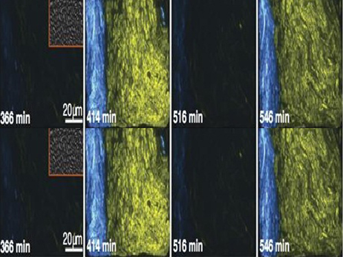
Figure 1: Metabolic engineering strategies for 1,3-diaminopropane production using C4 pathway
Figure 2: Fed-batch fermentation profiles of two final engineered E. coli strains
2015.08.12 View 11872
'Engineered Bacterium Produces 1,3-Diaminopropane'
A research team led by Distinguished Professor Sang Yup Lee of the Department of Chemical and Biomolecular Engineering at KAIST reported, for the first time, the production of 1,3-diaminopropane via fermentation of an engineered bacterium.
1,3-Diaminopropane is a three carbon diamine, which has a wide range of industrial applications including epoxy resin and cross-linking agents, as well as precursors for pharmaceuticals, agrochemicals, and organic chemicals. It can also be polymerized with dicarboxylic acids to make polyamides (nylons) for use as engineering plastics, medical materials, and adhesives.
Traditionally, 1,3-diaminopropane is derived from petroleum-based processes. In effort to address critical problems such as the depletion of petroleum and environmental issues inherent to the petroleum-based processes, the research team has developed an Escherichia coli (E. coli) strain capable of producing 1,3-diaminopropane. Using this technology, 1,3-diaminopropane can now be produced from renewable biomass instead of petroleum.
E. coli as found in nature is unable to produce 1,3-diaminopropane. Metabolic engineering, a technology to transform microorganisms into highly efficient microbial cell factories capable of producing chemical compounds of interest, was utilized to engineer the E. coli strain. First, naturally existing metabolic pathways for the biosynthesis of 1,3-diaminopropane were introduced into a virtual cell in silico to determine the most efficient metabolic pathway for the 1,3-diaminopropane production. The metabolic pathway selected was then introduced into an E. coli strain and successfully produced 1,3-diaminopropane for the first time in the world.
The research team applied metabolic engineering additionally, and the production titer of 1,3-diaminopropane increased about 21 fold. The Fed-batch fermentation of the engineered E. coli strain produced 13 grams per liter of 1,3-diaminoproapne. With this technology, 1,3-diaminopropane can be produced using renewable biomass, and it will be the starting point for replacing the current petroleum-based processes with bio-based processes.
Professor Lee said, “Our study suggested a possibility to produce 1,3-diaminopropane based on biorefinery. Further study will be done to increase the titer and productivity of 1,3-diaminopropane.”
This work was published online in Scientific Reports on August 11, 2015.
Reference: Chae, T.U. et al. "Metabolic engineering of Escherichia coli for the production of 1,3-diaminopropane, a three carbon diamine," Scientific Reports:
http://www.nature.com/articles/srep13040
This research was supported by the Technology Development Program to Solve Climate Changes on Systems Metabolic Engineering for Biorefineries from Ministry of Science, ICT and Future Planning (MSIP) through the National Research Foundation (NRF) of Korea.
Figure 1: Metabolic engineering strategies for 1,3-diaminopropane production using C4 pathway
Figure 2: Fed-batch fermentation profiles of two final engineered E. coli strains
2015.08.12 View 11872 -
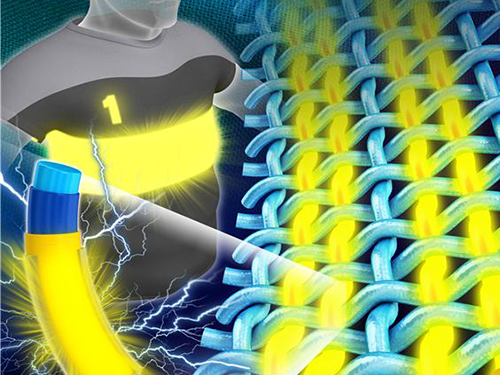 KAIST Develops Fiber-Like Light-Emitting Diodes for Wearable Displays
Professor Kyung-Cheol Choi and his research team from the School of Electrical Engineering at KAIST have developed fiber-like light-emitting diodes (LEDs), which can be applied in wearable displays. The research findings were published online in the July 14th issue of Advanced Electronic Materials.
Traditional wearable displays were manufactured on a hard substrate, which was later attached to the surface of clothes. This technique had limited applications for wearable displays because they were inflexible and ignored the characteristics of fabric.
To solve this problem, the research team discarded the notion of creating light-emitting diode displays on a plane. Instead, they focused on fibers, a component of fabrics, and developed a fiber-like LED that shared the characteristics of both fabrics and displays.
The essence of this technology, the dip-coating process, is to immerse and extract a three dimensional (3-D) rod (a polyethylene terephthalate fiber) from a solution, which functions like thread. Then, the regular levels of organic materials are formed as layers on the thread.
The dip-coating process allows the layers of organic materials to be easily created on the fibers with a 3-D cylindrical structure, which had been difficult in existing processes such as heat-coating process. By controlling of the withdrawal rate of the fiber, the coating's thickness can also be adjusted to the hundreds of thousandths of a nanometer.
The researchers said that this technology would accelerate the commercialization of fiber-based wearable displays because it offers low-cost mass production using roll-to-roll processing, a technology applied to create electronic devices on a roll of flexible plastics or metal foils.
Professor Choi said, “Our research will become a core technology in developing light emitting diodes on fibers, which are fundamental elements of fabrics. We hope we can lower the barrier of wearable displays entering the market.”
The lead author of the published paper, Seon-Il Kwon, added, “This technology will eventually allow the production of wearable displays to be as easy as making clothes.”
Picture 1: The Next Generation Wearable Display Using Fiber-Based Light-Emitting Diodes
Picture 2: Dip-Coating Process to Create Fiber-Based Light-Emitting Diodes
Picture 3: Fiber-Based Light-Emitting Diodes
2015.08.11 View 13768
KAIST Develops Fiber-Like Light-Emitting Diodes for Wearable Displays
Professor Kyung-Cheol Choi and his research team from the School of Electrical Engineering at KAIST have developed fiber-like light-emitting diodes (LEDs), which can be applied in wearable displays. The research findings were published online in the July 14th issue of Advanced Electronic Materials.
Traditional wearable displays were manufactured on a hard substrate, which was later attached to the surface of clothes. This technique had limited applications for wearable displays because they were inflexible and ignored the characteristics of fabric.
To solve this problem, the research team discarded the notion of creating light-emitting diode displays on a plane. Instead, they focused on fibers, a component of fabrics, and developed a fiber-like LED that shared the characteristics of both fabrics and displays.
The essence of this technology, the dip-coating process, is to immerse and extract a three dimensional (3-D) rod (a polyethylene terephthalate fiber) from a solution, which functions like thread. Then, the regular levels of organic materials are formed as layers on the thread.
The dip-coating process allows the layers of organic materials to be easily created on the fibers with a 3-D cylindrical structure, which had been difficult in existing processes such as heat-coating process. By controlling of the withdrawal rate of the fiber, the coating's thickness can also be adjusted to the hundreds of thousandths of a nanometer.
The researchers said that this technology would accelerate the commercialization of fiber-based wearable displays because it offers low-cost mass production using roll-to-roll processing, a technology applied to create electronic devices on a roll of flexible plastics or metal foils.
Professor Choi said, “Our research will become a core technology in developing light emitting diodes on fibers, which are fundamental elements of fabrics. We hope we can lower the barrier of wearable displays entering the market.”
The lead author of the published paper, Seon-Il Kwon, added, “This technology will eventually allow the production of wearable displays to be as easy as making clothes.”
Picture 1: The Next Generation Wearable Display Using Fiber-Based Light-Emitting Diodes
Picture 2: Dip-Coating Process to Create Fiber-Based Light-Emitting Diodes
Picture 3: Fiber-Based Light-Emitting Diodes
2015.08.11 View 13768 -
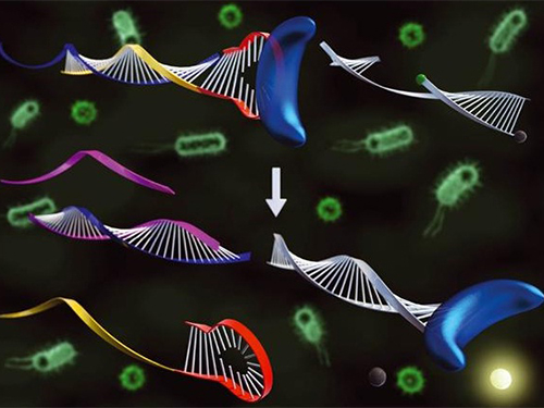 Affordable Genetic Diagnostic Technique for Target DNA Analysis Developed
Professor Hyun-Gyu Park of the Department of Chemical and Biomolecular Engineering at KAIST has developed a technique to analyze various target DNAs using an aptamer, a DNA fragment that can recognize and bind to a specific protein or enzyme. This technique will allow the development of affordable genetic diagnoses for new bacteria or virus, such as Middle Ease Respiratory Syndrome (MERS). The research findings were published in the June issue of Chemical Communications, issued by the Royal Society of Chemistry in the United Kingdom. The paper was selected as a lead article of the journal.
The existing genetic diagnosis technique, based on molecular beacon probes, requires a new beacon probe whenever a target DNA mutates. As a result, it was costly to analyze various target DNA fragments. To address this problem, Professor Park’s team designed an aptamer that binds and deactivates DNA polymerase. The technique was used in reverse, so that the aptemer did not bind to the polymerase, maintaining its activated state, only if the target DNA was present. These probes are called TagMan probes.
The controlled activation and deactivation of DNA polymerase enables nucleic acid to elongate or dwindle, making it possible to measure fluorescence signals coming from TaqMan probes. This same probe can be used to detect various target DNAs, leading to the development of a new and sensitive genetic diagnostic technique.
Unlike the existing molecular beacon probe technique which requires a new probe for every target DNA, this new technique uses the same fluorescent TaqMan probe, which is cheaper and easier to detect a number of different target nucleic acid fragments. The application of this technique will make the process of identifying and detecting foreign DNAs from pathogens such as virus and bacteria more affordable and simple.
Professor Park said, “This technique will enable us to develop simpler diagnostic kits for new pathogens, such as MERS, allowing a faster response to various diseases. Our technology can also be applied widely in the field of genetic diagnostics.”
Picture: A schematic image of target nucleic acid extracted through the activation and deactivation of DNA polymerase
2015.07.31 View 11002
Affordable Genetic Diagnostic Technique for Target DNA Analysis Developed
Professor Hyun-Gyu Park of the Department of Chemical and Biomolecular Engineering at KAIST has developed a technique to analyze various target DNAs using an aptamer, a DNA fragment that can recognize and bind to a specific protein or enzyme. This technique will allow the development of affordable genetic diagnoses for new bacteria or virus, such as Middle Ease Respiratory Syndrome (MERS). The research findings were published in the June issue of Chemical Communications, issued by the Royal Society of Chemistry in the United Kingdom. The paper was selected as a lead article of the journal.
The existing genetic diagnosis technique, based on molecular beacon probes, requires a new beacon probe whenever a target DNA mutates. As a result, it was costly to analyze various target DNA fragments. To address this problem, Professor Park’s team designed an aptamer that binds and deactivates DNA polymerase. The technique was used in reverse, so that the aptemer did not bind to the polymerase, maintaining its activated state, only if the target DNA was present. These probes are called TagMan probes.
The controlled activation and deactivation of DNA polymerase enables nucleic acid to elongate or dwindle, making it possible to measure fluorescence signals coming from TaqMan probes. This same probe can be used to detect various target DNAs, leading to the development of a new and sensitive genetic diagnostic technique.
Unlike the existing molecular beacon probe technique which requires a new probe for every target DNA, this new technique uses the same fluorescent TaqMan probe, which is cheaper and easier to detect a number of different target nucleic acid fragments. The application of this technique will make the process of identifying and detecting foreign DNAs from pathogens such as virus and bacteria more affordable and simple.
Professor Park said, “This technique will enable us to develop simpler diagnostic kits for new pathogens, such as MERS, allowing a faster response to various diseases. Our technology can also be applied widely in the field of genetic diagnostics.”
Picture: A schematic image of target nucleic acid extracted through the activation and deactivation of DNA polymerase
2015.07.31 View 11002 -
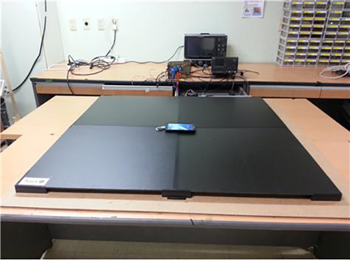 Omnidirectional Free Space Wireless Charging Developed
The simultaneous charging of multiple mobile devices at 0.5 meter away from the power source is now possible under the international electromagnetic field guidelines.
Mobile devices, such as smartphones and laptops, have become indispensable portable items in modern life, but one big challenge remains to fully enjoying these devices: keeping their batteries charged.
A group of researchers at KAIST has developed a wireless-power transfer (WPT) technology that allows mobile devices to be charged at any location and in any direction, even if the devices are away from the power source, just as Wi-Fi works for Internet connections. With this technology, so long as mobile users stay in a designated area where the charging is available, e.g., the Wi-Power zone, the device, without being tethered to a charger, will pick up power automatically, as needed.
The research team led by Professor Chun T. Rim of the Nuclear and Quantum Engineering Department at KAIST has made great strides in WPT development. Their WPT system is capable of charging multiple mobile devices concurrently and with unprecedented freedom in any direction, even while holding the devices in midair or a half meter away from the power source, which is a transmitter. The research result was published in the June 2015 on-line issue of IEEE Transactions on Power Electronics, which is entitled “Six Degrees of Freedom Mobile Inductive Power Transfer by Crossed Dipole Tx (Transmitter) and Rx (Receiver) Coils.”
Professor Rim’s team has successfully showcased the technology on July 7, 2015 at a lab on KAIST’s campus. They used high-frequency magnetic materials in a dipole coil structure to build a thin, flat transmitter (Tx) system shaped in a rectangle with a size of 1m2. Either 30 smartphones with a power capacity of one watt each or 5 laptops with 2.4 watts each can be simultaneously and wirelessly charged at a 50 cm distance from the transmitter with six degrees of freedom, regardless of the devices’ three-axes positions and directions. This means that the device can receive power all around the transmitter in three-dimensional space. The maximum power transfer efficiency for the laptops was 34%. The researchers said that to fabricate plane Tx and Rx coils with the six-degree-of-freedom characteristic was a bottleneck of WPT for mobile applications.
Dipole Coil Resonance System (DCRS)
The research team used the Dipole Coil Resonance System (DCRS) to induce magnetic fields, which was developed by the team in 2014 for inductive power transfer over an extended distance. The DCRS is composed of two (transmitting and receiving) magnetic dipole coils, placed in parallel, with each coil having a ferrite core and connected with a resonant capacitor. Comparing to a conventional loop coil, the dipole coil is very compact and has a less dimension. Therefore, a crossed dipole structure has 2-dimension rather than 3-dimension of a crossed loop coil structure. The DCRS has a great advantage to transfer power even when the resonance frequency changes in the range of 1% (Q factor is below 100). The ferrite cores are optimally designed to reduce the core volume by half, and their ability to transfer power is nearly unaffected by human bodies or surrounding metal objects, making DCRS ideal to transmit wireless power in emergency situations. In a test conducted in 2014, Professor Rim succeeded in transferring 209 watts of power wirelessly to the distance of five meters. (See KAIST’s press release on DCRS for details: http://www.eurekalert.org/pub_releases/2014-04/tkai-wpt041714.php.)
Greater Flexibility and Safer Charging
The research team rearranged the two dipole coils from a parallel position to cross them in order to generate rotating magnetic fields, which was embedded in the Tx’s flat platform. This has made it possible for mobile devices to receive power from any direction.
Although wireless-power technology has been applied to smartphones, it could not offer any substantial advantages over traditional wired charging because the devices still require close contact with the transmitter, a charging pad. To use the devices freely and safely, including in public spaces, the WPT technology should provide mobile users with six degrees of freedom at a distance. Until now, all wireless-charging technologies have had difficulties with the problem of short charging distance, mostly less than 10 cm, as well as charging conditions that the devices should be placed in a fixed position. For example, the Galaxy S6 could only be charged wirelessly in a fixed position, having one degree of freedom. The degree of freedom represents mobile devices’ freedom of movement in three-dimensional space.
In addition, the DCRS works at a low magnetic field environment. Based on the magnetic flux shielding technology developed by the research team, the level of magnetic flux is below the safety level of the International Commission on Non-Ionizing Radiation Protection (ICNIRP) guideline (27µT) for general public exposure to electromagnetic field (EMF).
Professor Rim said, “Our transmitter system is safe for humans and compatible with other electronic devices. We have solved three major issues of short charging distance, the dependence on charging directions, and plane coil structures of both Tx and Rx, which have blocked the commercialization of WPT.”
Currently, the research team and KAIST’s spin-off company, TESLAS, Inc., have been conducting pilot projects to apply DCRS in various places such as cafes and offices.
YouTube Link: https://www.youtube.com/watch?v=JU64pMyJioc
Demonstration of 30 Watts Range Omnidirectional Wireless-charging at a Laboratory on KAIST’s Campus
Figure 1: Wide-range omnidirectional wireless-charging system based on DCRS can charge multiple numbers of mobile devices simultaneously in a 1m3 range. The above is a transmitter, and the below is a Samsung Galaxy Note with a receiver embedded inside.
Figure 2: Demonstration of the omnidirectional wireless-charging system (clockwise from top of the left, robust charging despite the presence of metal obstacles, omnidirectional charging, long distance charging, and multiple devices charging)
2015.07.08 View 17524
Omnidirectional Free Space Wireless Charging Developed
The simultaneous charging of multiple mobile devices at 0.5 meter away from the power source is now possible under the international electromagnetic field guidelines.
Mobile devices, such as smartphones and laptops, have become indispensable portable items in modern life, but one big challenge remains to fully enjoying these devices: keeping their batteries charged.
A group of researchers at KAIST has developed a wireless-power transfer (WPT) technology that allows mobile devices to be charged at any location and in any direction, even if the devices are away from the power source, just as Wi-Fi works for Internet connections. With this technology, so long as mobile users stay in a designated area where the charging is available, e.g., the Wi-Power zone, the device, without being tethered to a charger, will pick up power automatically, as needed.
The research team led by Professor Chun T. Rim of the Nuclear and Quantum Engineering Department at KAIST has made great strides in WPT development. Their WPT system is capable of charging multiple mobile devices concurrently and with unprecedented freedom in any direction, even while holding the devices in midair or a half meter away from the power source, which is a transmitter. The research result was published in the June 2015 on-line issue of IEEE Transactions on Power Electronics, which is entitled “Six Degrees of Freedom Mobile Inductive Power Transfer by Crossed Dipole Tx (Transmitter) and Rx (Receiver) Coils.”
Professor Rim’s team has successfully showcased the technology on July 7, 2015 at a lab on KAIST’s campus. They used high-frequency magnetic materials in a dipole coil structure to build a thin, flat transmitter (Tx) system shaped in a rectangle with a size of 1m2. Either 30 smartphones with a power capacity of one watt each or 5 laptops with 2.4 watts each can be simultaneously and wirelessly charged at a 50 cm distance from the transmitter with six degrees of freedom, regardless of the devices’ three-axes positions and directions. This means that the device can receive power all around the transmitter in three-dimensional space. The maximum power transfer efficiency for the laptops was 34%. The researchers said that to fabricate plane Tx and Rx coils with the six-degree-of-freedom characteristic was a bottleneck of WPT for mobile applications.
Dipole Coil Resonance System (DCRS)
The research team used the Dipole Coil Resonance System (DCRS) to induce magnetic fields, which was developed by the team in 2014 for inductive power transfer over an extended distance. The DCRS is composed of two (transmitting and receiving) magnetic dipole coils, placed in parallel, with each coil having a ferrite core and connected with a resonant capacitor. Comparing to a conventional loop coil, the dipole coil is very compact and has a less dimension. Therefore, a crossed dipole structure has 2-dimension rather than 3-dimension of a crossed loop coil structure. The DCRS has a great advantage to transfer power even when the resonance frequency changes in the range of 1% (Q factor is below 100). The ferrite cores are optimally designed to reduce the core volume by half, and their ability to transfer power is nearly unaffected by human bodies or surrounding metal objects, making DCRS ideal to transmit wireless power in emergency situations. In a test conducted in 2014, Professor Rim succeeded in transferring 209 watts of power wirelessly to the distance of five meters. (See KAIST’s press release on DCRS for details: http://www.eurekalert.org/pub_releases/2014-04/tkai-wpt041714.php.)
Greater Flexibility and Safer Charging
The research team rearranged the two dipole coils from a parallel position to cross them in order to generate rotating magnetic fields, which was embedded in the Tx’s flat platform. This has made it possible for mobile devices to receive power from any direction.
Although wireless-power technology has been applied to smartphones, it could not offer any substantial advantages over traditional wired charging because the devices still require close contact with the transmitter, a charging pad. To use the devices freely and safely, including in public spaces, the WPT technology should provide mobile users with six degrees of freedom at a distance. Until now, all wireless-charging technologies have had difficulties with the problem of short charging distance, mostly less than 10 cm, as well as charging conditions that the devices should be placed in a fixed position. For example, the Galaxy S6 could only be charged wirelessly in a fixed position, having one degree of freedom. The degree of freedom represents mobile devices’ freedom of movement in three-dimensional space.
In addition, the DCRS works at a low magnetic field environment. Based on the magnetic flux shielding technology developed by the research team, the level of magnetic flux is below the safety level of the International Commission on Non-Ionizing Radiation Protection (ICNIRP) guideline (27µT) for general public exposure to electromagnetic field (EMF).
Professor Rim said, “Our transmitter system is safe for humans and compatible with other electronic devices. We have solved three major issues of short charging distance, the dependence on charging directions, and plane coil structures of both Tx and Rx, which have blocked the commercialization of WPT.”
Currently, the research team and KAIST’s spin-off company, TESLAS, Inc., have been conducting pilot projects to apply DCRS in various places such as cafes and offices.
YouTube Link: https://www.youtube.com/watch?v=JU64pMyJioc
Demonstration of 30 Watts Range Omnidirectional Wireless-charging at a Laboratory on KAIST’s Campus
Figure 1: Wide-range omnidirectional wireless-charging system based on DCRS can charge multiple numbers of mobile devices simultaneously in a 1m3 range. The above is a transmitter, and the below is a Samsung Galaxy Note with a receiver embedded inside.
Figure 2: Demonstration of the omnidirectional wireless-charging system (clockwise from top of the left, robust charging despite the presence of metal obstacles, omnidirectional charging, long distance charging, and multiple devices charging)
2015.07.08 View 17524 -
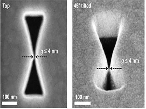 3D Plasmon Antenna Capable of Focusing Light into Few Nanometers
Professors Myung-Ki Kim and Yong-Hee Lee, both of the Physics Department at KAIST, and their research teams have developed a three dimensional (3D) gap-plasmon antenna which can focus light into a space a few nanometers wide. Their research findings were published in the June 10th issue of Nano Letters.
Focusing light into a point-like space is an active research field with many applications. However, concentrating light into a smaller space than its wavelength is often hindered by diffraction. To tackle this problem, many researchers have utilized the plasmonic phenomenon of a metal where light can be confined to a greater extent by overcoming the diffraction limit.
Many researchers have focused on developing a two dimensional (2D) plasmon antenna and were able to focus a light under 5 nanometers wide. However, this 2D antenna revealed a challenge: the light disperses to the opposite end regardless of how small its beam was focused. To solve this difficulty, a 3D structure had to be employed to maximize the light's intensity.
Adopting the proximal focused-ion-beam milling technology, the KAIST research team developed a 3D four nanometer wide gap-plasmon antenna. By squeezing the photons into a 3D nano space of 4 x 10 x 10 nm3 size, the researchers were able to increase the intensity of light by 400,000 times stronger than that of the incident light. Capitalizing on the enhanced intensity of light within the antenna, they intensified the second-harmonic signal and verified that the light was focused in the nano gap by scanning cathodoluminescent images.
The researchers anticipate that this technology will improve the speed of data transfer and processing up to the level of a terahertz (one trillion times per second) and to enlarge the storage volume per unit area on hard disks by 100 times. In addition, high definition images of submolecule size can be taken with actual light, instead of with an electron microscope, while improving the semiconductor process to a smaller size of few nanometers.
Professor Kim said, “A simple yet ingenious idea has shifted the research paradigm from 2D gap-plasmon antennas to 3D antennas. This technology will see numerous applications including in the field of information technology, data storage, imaging medical science, and semiconductor processes.”
The research was sponsored by the National Research Foundation of Korea.
Figure 1: 3D Gap-Plasmon Antenna Structure and Simulation Results
Figure 2 – Constructed 3D Gap-Plasmon Antenna Structure
Figure 3 – Amplified Second Harmonic Signal Generation and Light Focused in the Nano Gap
2015.06.24 View 10988
3D Plasmon Antenna Capable of Focusing Light into Few Nanometers
Professors Myung-Ki Kim and Yong-Hee Lee, both of the Physics Department at KAIST, and their research teams have developed a three dimensional (3D) gap-plasmon antenna which can focus light into a space a few nanometers wide. Their research findings were published in the June 10th issue of Nano Letters.
Focusing light into a point-like space is an active research field with many applications. However, concentrating light into a smaller space than its wavelength is often hindered by diffraction. To tackle this problem, many researchers have utilized the plasmonic phenomenon of a metal where light can be confined to a greater extent by overcoming the diffraction limit.
Many researchers have focused on developing a two dimensional (2D) plasmon antenna and were able to focus a light under 5 nanometers wide. However, this 2D antenna revealed a challenge: the light disperses to the opposite end regardless of how small its beam was focused. To solve this difficulty, a 3D structure had to be employed to maximize the light's intensity.
Adopting the proximal focused-ion-beam milling technology, the KAIST research team developed a 3D four nanometer wide gap-plasmon antenna. By squeezing the photons into a 3D nano space of 4 x 10 x 10 nm3 size, the researchers were able to increase the intensity of light by 400,000 times stronger than that of the incident light. Capitalizing on the enhanced intensity of light within the antenna, they intensified the second-harmonic signal and verified that the light was focused in the nano gap by scanning cathodoluminescent images.
The researchers anticipate that this technology will improve the speed of data transfer and processing up to the level of a terahertz (one trillion times per second) and to enlarge the storage volume per unit area on hard disks by 100 times. In addition, high definition images of submolecule size can be taken with actual light, instead of with an electron microscope, while improving the semiconductor process to a smaller size of few nanometers.
Professor Kim said, “A simple yet ingenious idea has shifted the research paradigm from 2D gap-plasmon antennas to 3D antennas. This technology will see numerous applications including in the field of information technology, data storage, imaging medical science, and semiconductor processes.”
The research was sponsored by the National Research Foundation of Korea.
Figure 1: 3D Gap-Plasmon Antenna Structure and Simulation Results
Figure 2 – Constructed 3D Gap-Plasmon Antenna Structure
Figure 3 – Amplified Second Harmonic Signal Generation and Light Focused in the Nano Gap
2015.06.24 View 10988 -
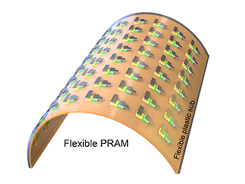 KAIST Team Develops Flexible PRAM
Phase change random access memory (PRAM) is one of the strongest candidates for next-generation nonvolatile memory for flexible and wearable electronics. In order to be used as a core memory for flexible devices, the most important issue is reducing high operating current. The effective solution is to decrease cell size in sub-micron region as in commercialized conventional PRAM. However, the scaling to nano-dimension on flexible substrates is extremely difficult due to soft nature and photolithographic limits on plastics, thus practical flexible PRAM has not been realized yet.
Recently, a team led by Professors Keon Jae Lee and Yeon Sik Jung of the Department of Materials Science and Engineering at KAIST has developed the first flexible PRAM enabled by self-assembled block copolymer (BCP) silica nanostructures with an ultralow current operation (below one quarter of conventional PRAM without BCP) on plastic substrates. BCP is the mixture of two different polymer materials, which can easily create self-ordered arrays of sub-20 nm features through simple spin-coating and plasma treatments. BCP silica nanostructures successfully lowered the contact area by localizing the volume change of phase-change materials and thus resulted in significant power reduction. Furthermore, the ultrathin silicon-based diodes were integrated with phase-change memories (PCM) to suppress the inter-cell interference, which demonstrated random access capability for flexible and wearable electronics. Their work was published in the March issue of ACS Nano: "Flexible One Diode-One Phase Change Memory Array Enabled by Block Copolymer Self-Assembly."
Another way to achieve ultralow-powered PRAM is to utilize self-structured conductive filaments (CF) instead of the resistor-type conventional heater. The self-structured CF nanoheater originated from unipolar memristor can generate strong heat toward phase-change materials due to high current density through the nanofilament. This ground-breaking methodology shows that sub-10 nm filament heater, without using expensive and non-compatible nanolithography, achieved nanoscale switching volume of phase change materials, resulted in the PCM writing current of below 20 uA, the lowest value among top-down PCM devices. This achievement was published in the June online issue of ACS Nano: "Self-Structured Conductive Filament Nanoheater for Chalcogenide Phase Transition." In addition, due to self-structured low-power technology compatible to plastics, the research team has recently succeeded in fabricating a flexible PRAM on wearable substrates.
Professor Lee said, "The demonstration of low power PRAM on plastics is one of the most important issues for next-generation wearable and flexible non-volatile memory. Our innovative and simple methodology represents the strong potential for commercializing flexible PRAM."
In addition, he wrote a review paper regarding the nanotechnology-based electronic devices in the June online issue of Advanced Materials entitled "Performance Enhancement of Electronic and Energy Devices via Block Copolymer Self-Assembly."
Picture Caption:
Low-power nonvolatile PRAM for flexible and wearable memories enabled by (a) self-assembled BCP silica nanostructures and (b) self-structured conductive filament nanoheater.
2015.06.15 View 16104
KAIST Team Develops Flexible PRAM
Phase change random access memory (PRAM) is one of the strongest candidates for next-generation nonvolatile memory for flexible and wearable electronics. In order to be used as a core memory for flexible devices, the most important issue is reducing high operating current. The effective solution is to decrease cell size in sub-micron region as in commercialized conventional PRAM. However, the scaling to nano-dimension on flexible substrates is extremely difficult due to soft nature and photolithographic limits on plastics, thus practical flexible PRAM has not been realized yet.
Recently, a team led by Professors Keon Jae Lee and Yeon Sik Jung of the Department of Materials Science and Engineering at KAIST has developed the first flexible PRAM enabled by self-assembled block copolymer (BCP) silica nanostructures with an ultralow current operation (below one quarter of conventional PRAM without BCP) on plastic substrates. BCP is the mixture of two different polymer materials, which can easily create self-ordered arrays of sub-20 nm features through simple spin-coating and plasma treatments. BCP silica nanostructures successfully lowered the contact area by localizing the volume change of phase-change materials and thus resulted in significant power reduction. Furthermore, the ultrathin silicon-based diodes were integrated with phase-change memories (PCM) to suppress the inter-cell interference, which demonstrated random access capability for flexible and wearable electronics. Their work was published in the March issue of ACS Nano: "Flexible One Diode-One Phase Change Memory Array Enabled by Block Copolymer Self-Assembly."
Another way to achieve ultralow-powered PRAM is to utilize self-structured conductive filaments (CF) instead of the resistor-type conventional heater. The self-structured CF nanoheater originated from unipolar memristor can generate strong heat toward phase-change materials due to high current density through the nanofilament. This ground-breaking methodology shows that sub-10 nm filament heater, without using expensive and non-compatible nanolithography, achieved nanoscale switching volume of phase change materials, resulted in the PCM writing current of below 20 uA, the lowest value among top-down PCM devices. This achievement was published in the June online issue of ACS Nano: "Self-Structured Conductive Filament Nanoheater for Chalcogenide Phase Transition." In addition, due to self-structured low-power technology compatible to plastics, the research team has recently succeeded in fabricating a flexible PRAM on wearable substrates.
Professor Lee said, "The demonstration of low power PRAM on plastics is one of the most important issues for next-generation wearable and flexible non-volatile memory. Our innovative and simple methodology represents the strong potential for commercializing flexible PRAM."
In addition, he wrote a review paper regarding the nanotechnology-based electronic devices in the June online issue of Advanced Materials entitled "Performance Enhancement of Electronic and Energy Devices via Block Copolymer Self-Assembly."
Picture Caption:
Low-power nonvolatile PRAM for flexible and wearable memories enabled by (a) self-assembled BCP silica nanostructures and (b) self-structured conductive filament nanoheater.
2015.06.15 View 16104 -
 KAIST-Taiwanese Team: Zinc Supplements May Help Treat Autism
A KAIST and Taiwanese research team has recently discovered strong evidence that Zinc is associated with autism spectrum disorders (ASD) and improves social interaction in mouse models with ASD. The research findings, titled “Trans-synaptic zinc mobilization improves social interaction in two mouse models of autism through NMDAR activation,” were published in Nature Communications on May 18, 2015. For details, please see an article below:
The China Post, June 4, 2015
“Zinc supplements may help treat autism: study”
http://www.chinapost.com.tw/health/mental-health/2015/06/04/437612/Zinc-suppliments.htm
2015.06.04 View 6981
KAIST-Taiwanese Team: Zinc Supplements May Help Treat Autism
A KAIST and Taiwanese research team has recently discovered strong evidence that Zinc is associated with autism spectrum disorders (ASD) and improves social interaction in mouse models with ASD. The research findings, titled “Trans-synaptic zinc mobilization improves social interaction in two mouse models of autism through NMDAR activation,” were published in Nature Communications on May 18, 2015. For details, please see an article below:
The China Post, June 4, 2015
“Zinc supplements may help treat autism: study”
http://www.chinapost.com.tw/health/mental-health/2015/06/04/437612/Zinc-suppliments.htm
2015.06.04 View 6981 -
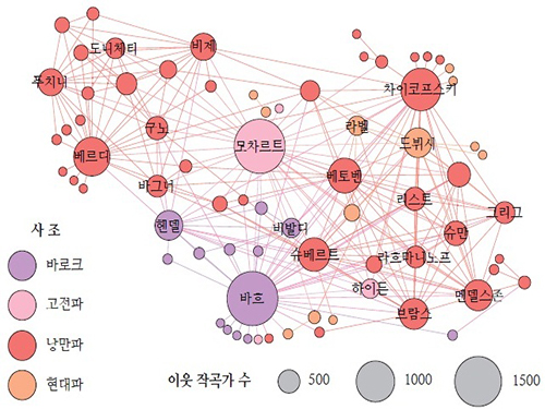 Big Data Reveals the Secret of Classical Music Creation
Professor Juyong Park of the Graduate School of Culture Technology at KAIST and his research team have recently published the result of their study (“Topology and Evolution of the Network of Western Classical Music Composers”) on the dynamics of how classical music is created, stylized, and disseminated in EPJ Data Science online on April 22, 2015. For the press release issued by the journal, please go to the link below:
EPJ Data Science, May 6, 2015
“EPJ Data Science Highlight—Big Data Reveals Classical Music Creation Secrets”
http://www.epj.org/113-epj-ds/941-epjds-highlight-big-data-reveals-classical-music-creation-secrets
Researchers used big-data analysis and modelling technique to examine the complex, undercurrent network of classical music composers, which was constructed from the large volume of compact disc (CD) recordings data collected from an online retailer, ArkivMusic, and a music reference website, AllMusicGuide.
The study discovered that the basic characteristics of composers’ network are similar to many real-world networks, including the small-world property, the existence of a giant component, high clustering, and heavy-tailed degree distributions. The research team also found that composers collaborated and influenced each other and that composers’ networks grew over time.
The research showed that consumers of classical music CDs tend to listen together to the music of a certain group of different composers, offering a useful tool to understand how the music style and market develops. Based on this, the research team predicted the future of the classical music market would be centered on top composers, while maintaining diversity due to the growing number of new composers.
Professor Park said, “In recent years, technology greatly affects the way we consume culture and art. Accordingly, we see more and more artists and institutions try to incorporate technology into their creative process, and this will lead us to larger- and higher-quality data that can allow us to learn more about culture and art. The quantitative methodology we have demonstrated in our research will give us an opportunity to explore the nature of art and literature in novel ways.”
The European Physical Journal (EPJ) comprises a series of peer-reviewed journals, eleven in total, which cover physics and related subjects such as The Large Hadron Collider, condensed matter, particles, soft matter, and biological physics. The EPJ Data Science is the latest journal launched by EPJ.
Figure: Backbone of the Composer Network
The composer-composer network backbone, projected from the CD-composer network, reveals the major component of the network. The node sizes represent the composers’ degrees, and the colors represent their active periods.
2015.05.07 View 11300
Big Data Reveals the Secret of Classical Music Creation
Professor Juyong Park of the Graduate School of Culture Technology at KAIST and his research team have recently published the result of their study (“Topology and Evolution of the Network of Western Classical Music Composers”) on the dynamics of how classical music is created, stylized, and disseminated in EPJ Data Science online on April 22, 2015. For the press release issued by the journal, please go to the link below:
EPJ Data Science, May 6, 2015
“EPJ Data Science Highlight—Big Data Reveals Classical Music Creation Secrets”
http://www.epj.org/113-epj-ds/941-epjds-highlight-big-data-reveals-classical-music-creation-secrets
Researchers used big-data analysis and modelling technique to examine the complex, undercurrent network of classical music composers, which was constructed from the large volume of compact disc (CD) recordings data collected from an online retailer, ArkivMusic, and a music reference website, AllMusicGuide.
The study discovered that the basic characteristics of composers’ network are similar to many real-world networks, including the small-world property, the existence of a giant component, high clustering, and heavy-tailed degree distributions. The research team also found that composers collaborated and influenced each other and that composers’ networks grew over time.
The research showed that consumers of classical music CDs tend to listen together to the music of a certain group of different composers, offering a useful tool to understand how the music style and market develops. Based on this, the research team predicted the future of the classical music market would be centered on top composers, while maintaining diversity due to the growing number of new composers.
Professor Park said, “In recent years, technology greatly affects the way we consume culture and art. Accordingly, we see more and more artists and institutions try to incorporate technology into their creative process, and this will lead us to larger- and higher-quality data that can allow us to learn more about culture and art. The quantitative methodology we have demonstrated in our research will give us an opportunity to explore the nature of art and literature in novel ways.”
The European Physical Journal (EPJ) comprises a series of peer-reviewed journals, eleven in total, which cover physics and related subjects such as The Large Hadron Collider, condensed matter, particles, soft matter, and biological physics. The EPJ Data Science is the latest journal launched by EPJ.
Figure: Backbone of the Composer Network
The composer-composer network backbone, projected from the CD-composer network, reveals the major component of the network. The node sizes represent the composers’ degrees, and the colors represent their active periods.
2015.05.07 View 11300 -
 Fast, Accurate 3D Imaging to Track Optically-Trapped Particles
KAIST researchers published an article on the development of a novel technique to precisely track the 3-D positions of optically-trapped particles having complicated geometry in high speed in the April 2015 issue of Optica.
Optical tweezers have been used as an invaluable tool for exerting micro-scale force on microscopic particles and manipulating three-dimensional (3-D) positions of particles. Optical tweezers employ a tightly-focused laser whose beam diameter is smaller than one micrometer (1/100 of hair thickness), which generates attractive force on neighboring microscopic particles moving toward the beam focus. Controlling the positions of the beam focus enabled researchers to hold the particles and move them freely to other locations so they coined the name “optical tweezers.”
To locate the optically-trapped particles by a laser beam, optical microscopes have usually been employed. Optical microscopes measure light signals scattered by the optically-trapped microscopic particles and the positions of the particles in two dimensions. However, it was difficult to quantify the particles’ precise positions along the optic axis, the direction of the beam, from a single image, which is analogous to the difficulty of determining the front and rear positions of objects when closing an eye due to a lack of depth perception. Furthermore, it became more difficult to measure precisely 3-D positions of particles when scattered light signals were distorted by optically-trapped particles having complicated shapes or other particles occlude the target object along the optic axis.
Professor YongKeun Park and his research team in the Department of Physics at the Korea Advanced Institute of Science and Technology (KAIST) employed an optical diffraction tomography (ODT) technique to measure 3-D positions of optically-trapped particles in high speed. The principle of ODT is similar to X-ray CT imaging commonly used in hospitals for visualizing the internal organs of patients. Like X-ray CT imaging, which takes several images from various illumination angles, ODT measures 3-D images of optically-trapped particles by illuminating them with a laser beam in various incidence angles.
The KAIST team used optical tweezers to trap a glass bead with a diameter of 2 micrometers, and moved the bead toward a white blood cell having complicated internal structures. The team measured the 3-D dynamics of the white blood cell as it responded to an approaching glass bead via ODT in the high acquisition rate of 60 images per second. Since the white blood cell screens the glass bead along an optic axis, a conventionally-used optical microscope could not determine the 3-D positions of the glass bead. In contrast, the present method employing ODT localized the 3-D positions of the bead precisely as well as measured the composition of the internal materials of the bead and the white blood cell simultaneously.
Professor Park said, “Our technique has the advantage of measuring the 3-D positions and internal structures of optically-trapped particles in high speed without labelling exogenous fluorescent agents and can be applied in various fields including physics, optics, nanotechnology, and medical science.”
Kyoohyun Kim, the lead author of this paper (“Simultaneous 3D Visualization and Position Tracking of Optically Trapped Particles Using Optical Diffraction Tomography”), added, “This ODT technique can also apply to cellular-level surgeries where optical tweezers are used to manipulate intracellular organelles and to display in real time and in 3-D the images of the reaction of the cell membrane and nucleus during the operation or monitoring the recovery process of the cells from the surgery.”
The research results were published as the cover article in the April 2014 issue of Optica, the newest journal launched last year by the Optical Society of America (OSA) for rapid dissemination of high-impact results related to optics.
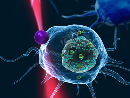
Figure 1: This picture shows the concept image of tweezing an optically-trapped glass bead on the cellular membrane of a white blood cell.
Figure 2: High-speed 3-D images produced from optical diffraction tomography technique
2015.04.24 View 12665
Fast, Accurate 3D Imaging to Track Optically-Trapped Particles
KAIST researchers published an article on the development of a novel technique to precisely track the 3-D positions of optically-trapped particles having complicated geometry in high speed in the April 2015 issue of Optica.
Optical tweezers have been used as an invaluable tool for exerting micro-scale force on microscopic particles and manipulating three-dimensional (3-D) positions of particles. Optical tweezers employ a tightly-focused laser whose beam diameter is smaller than one micrometer (1/100 of hair thickness), which generates attractive force on neighboring microscopic particles moving toward the beam focus. Controlling the positions of the beam focus enabled researchers to hold the particles and move them freely to other locations so they coined the name “optical tweezers.”
To locate the optically-trapped particles by a laser beam, optical microscopes have usually been employed. Optical microscopes measure light signals scattered by the optically-trapped microscopic particles and the positions of the particles in two dimensions. However, it was difficult to quantify the particles’ precise positions along the optic axis, the direction of the beam, from a single image, which is analogous to the difficulty of determining the front and rear positions of objects when closing an eye due to a lack of depth perception. Furthermore, it became more difficult to measure precisely 3-D positions of particles when scattered light signals were distorted by optically-trapped particles having complicated shapes or other particles occlude the target object along the optic axis.
Professor YongKeun Park and his research team in the Department of Physics at the Korea Advanced Institute of Science and Technology (KAIST) employed an optical diffraction tomography (ODT) technique to measure 3-D positions of optically-trapped particles in high speed. The principle of ODT is similar to X-ray CT imaging commonly used in hospitals for visualizing the internal organs of patients. Like X-ray CT imaging, which takes several images from various illumination angles, ODT measures 3-D images of optically-trapped particles by illuminating them with a laser beam in various incidence angles.
The KAIST team used optical tweezers to trap a glass bead with a diameter of 2 micrometers, and moved the bead toward a white blood cell having complicated internal structures. The team measured the 3-D dynamics of the white blood cell as it responded to an approaching glass bead via ODT in the high acquisition rate of 60 images per second. Since the white blood cell screens the glass bead along an optic axis, a conventionally-used optical microscope could not determine the 3-D positions of the glass bead. In contrast, the present method employing ODT localized the 3-D positions of the bead precisely as well as measured the composition of the internal materials of the bead and the white blood cell simultaneously.
Professor Park said, “Our technique has the advantage of measuring the 3-D positions and internal structures of optically-trapped particles in high speed without labelling exogenous fluorescent agents and can be applied in various fields including physics, optics, nanotechnology, and medical science.”
Kyoohyun Kim, the lead author of this paper (“Simultaneous 3D Visualization and Position Tracking of Optically Trapped Particles Using Optical Diffraction Tomography”), added, “This ODT technique can also apply to cellular-level surgeries where optical tweezers are used to manipulate intracellular organelles and to display in real time and in 3-D the images of the reaction of the cell membrane and nucleus during the operation or monitoring the recovery process of the cells from the surgery.”
The research results were published as the cover article in the April 2014 issue of Optica, the newest journal launched last year by the Optical Society of America (OSA) for rapid dissemination of high-impact results related to optics.
Figure 1: This picture shows the concept image of tweezing an optically-trapped glass bead on the cellular membrane of a white blood cell.
Figure 2: High-speed 3-D images produced from optical diffraction tomography technique
2015.04.24 View 12665 -
 KAIST Researchers Develops Hyper-Stretchable Elastic-Composite Energy Harvester
A research team led by Professor Keon Jae Lee (http://fand.kaist.ac.kr) of the Department of Materials Science and Engineering at KAIST has developed a hyper-stretchable elastic-composite energy harvesting device called a nanogenerator.
Flexible electronics have come into the market and are enabling new technologies like flexible displays in mobile phone, wearable electronics, and the Internet of Things (IoTs). However, is the degree of flexibility enough for most applications? For many flexible devices, elasticity is a very important issue. For example, wearable/biomedical devices and electronic skins (e-skins) should stretch to conform to arbitrarily curved surfaces and moving body parts such as joints, diaphragms, and tendons. They must be able to withstand the repeated and prolonged mechanical stresses of stretching. In particular, the development of elastic energy devices is regarded as critical to establish power supplies in stretchable applications. Although several researchers have explored diverse stretchable electronics, due to the absence of the appropriate device structures and correspondingly electrodes, researchers have not developed ultra-stretchable and fully-reversible energy conversion devices properly.
Recently, researchers from KAIST and Seoul National University (SNU) have collaborated and demonstrated a facile methodology to obtain a high-performance and hyper-stretchable elastic-composite generator (SEG) using very long silver nanowire-based stretchable electrodes. Their stretchable piezoelectric generator can harvest mechanical energy to produce high power output (~4 V) with large elasticity (~250%) and excellent durability (over 104 cycles). These noteworthy results were achieved by the non-destructive stress- relaxation ability of the unique electrodes as well as the good piezoelectricity of the device components. The new SEG can be applied to a wide-variety of wearable energy-harvesters to transduce biomechanical-stretching energy from the body (or machines) to electrical energy.
Professor Lee said, “This exciting approach introduces an ultra-stretchable piezoelectric generator. It can open avenues for power supplies in universal wearable and biomedical applications as well as self-powered ultra-stretchable electronics.”
This result was published online in the March issue of Advanced Materials, which is entitled “A Hyper-Stretchable Elastic-Composite Energy Harvester.”
YouTube Link: “A hyper-stretchable energy harvester”
https://www.youtube.com/watch?v=EBByFvPVRiU&feature=youtu.be
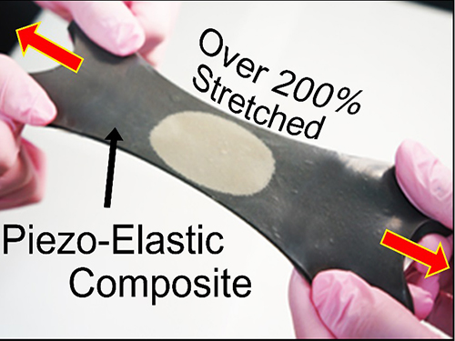
Figure: Top row: Schematics of hyper-stretchable elastic-composite generator enabled by very long silver nanowire-based stretchable electrodes.
Bottom row: The SEG energy harvester stretched by human hands over 200% strain.
2015.04.14 View 14705
KAIST Researchers Develops Hyper-Stretchable Elastic-Composite Energy Harvester
A research team led by Professor Keon Jae Lee (http://fand.kaist.ac.kr) of the Department of Materials Science and Engineering at KAIST has developed a hyper-stretchable elastic-composite energy harvesting device called a nanogenerator.
Flexible electronics have come into the market and are enabling new technologies like flexible displays in mobile phone, wearable electronics, and the Internet of Things (IoTs). However, is the degree of flexibility enough for most applications? For many flexible devices, elasticity is a very important issue. For example, wearable/biomedical devices and electronic skins (e-skins) should stretch to conform to arbitrarily curved surfaces and moving body parts such as joints, diaphragms, and tendons. They must be able to withstand the repeated and prolonged mechanical stresses of stretching. In particular, the development of elastic energy devices is regarded as critical to establish power supplies in stretchable applications. Although several researchers have explored diverse stretchable electronics, due to the absence of the appropriate device structures and correspondingly electrodes, researchers have not developed ultra-stretchable and fully-reversible energy conversion devices properly.
Recently, researchers from KAIST and Seoul National University (SNU) have collaborated and demonstrated a facile methodology to obtain a high-performance and hyper-stretchable elastic-composite generator (SEG) using very long silver nanowire-based stretchable electrodes. Their stretchable piezoelectric generator can harvest mechanical energy to produce high power output (~4 V) with large elasticity (~250%) and excellent durability (over 104 cycles). These noteworthy results were achieved by the non-destructive stress- relaxation ability of the unique electrodes as well as the good piezoelectricity of the device components. The new SEG can be applied to a wide-variety of wearable energy-harvesters to transduce biomechanical-stretching energy from the body (or machines) to electrical energy.
Professor Lee said, “This exciting approach introduces an ultra-stretchable piezoelectric generator. It can open avenues for power supplies in universal wearable and biomedical applications as well as self-powered ultra-stretchable electronics.”
This result was published online in the March issue of Advanced Materials, which is entitled “A Hyper-Stretchable Elastic-Composite Energy Harvester.”
YouTube Link: “A hyper-stretchable energy harvester”
https://www.youtube.com/watch?v=EBByFvPVRiU&feature=youtu.be
Figure: Top row: Schematics of hyper-stretchable elastic-composite generator enabled by very long silver nanowire-based stretchable electrodes.
Bottom row: The SEG energy harvester stretched by human hands over 200% strain.
2015.04.14 View 14705 -
 Anti-Cancer Therapy Delivering Drug to an Entire Tumor Developed
KAIST’s Department of Bio and Brain Engineering Professor Ji-Ho Park and his team successfully developed a new highly efficacious anti-cancer nanotechnology by delivering anti-cancer drugs uniformly to an entire tumor. Their research results were published in Nano Letters online on March 31, 2015.
To treat inoperable tumors, anti-cancer medicine is commonly used. However, efficient drug delivery to tumor cells is often difficult, treating an entire tumor with drugs even more so.
Using the existing drug delivery systems, including nanotechnology, a drug can be delivered only to tumor cells near blood vessels, leaving cells at the heart of a tumor intact. Since most drugs are injected into the bloodstream, tumor recurrence post medication is frequent.
Therefore, the team used liposomes that can fuse to the cell membrane and enter the cell. Once inside liposomes the drug can travel into the bloodstream, enter tumor cells near blood vessels, where they are loaded to exosomes, which are naturally occurring nanoparticles in the body. Since exosomes can travel between cells, the drug can be delivered efficiently into inner cells of the tumor.
Exosomes, which are secreted by cells that exist in the tumor microenvironment, is known to have an important role in tumor progression and metastasis since they transfer biological materials between cells. The research team started the investigation recognizing the possibility of delivering the anti-cancer drug to the entire tumor using exosomes.
The team injected the light-sensitive anti-cancer drug using their new delivery technique into experimental mice. The researchers applied light to the tumor site to activate the anti-cancer treatment and analyzed a tissue sample. They observed the effects of the anti-cancer drug in the entire tumor tissue.
The team’s results establish a ground-breaking foothold in drug delivery technology development that can be tailored to specific diseases by understanding its microenvironment. The work paves the way to more effective drug delivery systems for many chronic diseases, including cancer tumors that were difficult to treat due to the inability to penetrate deep into the tissue.
The team is currently conducting experiments with other anti-cancer drugs, which are being developed by pharmaceutical companies, using their tumor-penetrating drug delivery nanotechnology, to identify its effects on malignant tumors.
Professor Park said, “This research is the first to apply biological nanoparticles, exosomes that are continuously secreted and can transfer materials to neighboring cells, to deliver drugs directly to the heart of tumor.”
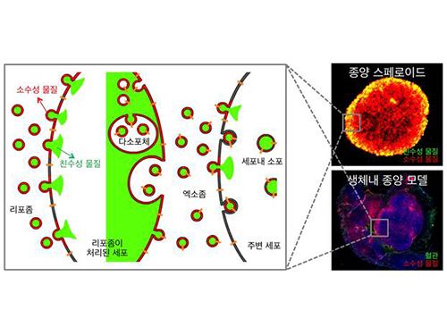
Picture: Incorporation of hydrophilic and hydrophobic compounds into membrane vesicles by engineering the parental cells via synthetic liposomes.
2015.04.07 View 12871
Anti-Cancer Therapy Delivering Drug to an Entire Tumor Developed
KAIST’s Department of Bio and Brain Engineering Professor Ji-Ho Park and his team successfully developed a new highly efficacious anti-cancer nanotechnology by delivering anti-cancer drugs uniformly to an entire tumor. Their research results were published in Nano Letters online on March 31, 2015.
To treat inoperable tumors, anti-cancer medicine is commonly used. However, efficient drug delivery to tumor cells is often difficult, treating an entire tumor with drugs even more so.
Using the existing drug delivery systems, including nanotechnology, a drug can be delivered only to tumor cells near blood vessels, leaving cells at the heart of a tumor intact. Since most drugs are injected into the bloodstream, tumor recurrence post medication is frequent.
Therefore, the team used liposomes that can fuse to the cell membrane and enter the cell. Once inside liposomes the drug can travel into the bloodstream, enter tumor cells near blood vessels, where they are loaded to exosomes, which are naturally occurring nanoparticles in the body. Since exosomes can travel between cells, the drug can be delivered efficiently into inner cells of the tumor.
Exosomes, which are secreted by cells that exist in the tumor microenvironment, is known to have an important role in tumor progression and metastasis since they transfer biological materials between cells. The research team started the investigation recognizing the possibility of delivering the anti-cancer drug to the entire tumor using exosomes.
The team injected the light-sensitive anti-cancer drug using their new delivery technique into experimental mice. The researchers applied light to the tumor site to activate the anti-cancer treatment and analyzed a tissue sample. They observed the effects of the anti-cancer drug in the entire tumor tissue.
The team’s results establish a ground-breaking foothold in drug delivery technology development that can be tailored to specific diseases by understanding its microenvironment. The work paves the way to more effective drug delivery systems for many chronic diseases, including cancer tumors that were difficult to treat due to the inability to penetrate deep into the tissue.
The team is currently conducting experiments with other anti-cancer drugs, which are being developed by pharmaceutical companies, using their tumor-penetrating drug delivery nanotechnology, to identify its effects on malignant tumors.
Professor Park said, “This research is the first to apply biological nanoparticles, exosomes that are continuously secreted and can transfer materials to neighboring cells, to deliver drugs directly to the heart of tumor.”
Picture: Incorporation of hydrophilic and hydrophobic compounds into membrane vesicles by engineering the parental cells via synthetic liposomes.
2015.04.07 View 12871