research
-
 Technology that will allow household scale position tracking of smartphones indoors, where GPS signals do not reach, has been developed. It is anticipated that the newly developed technology will enable the tracking of persons indoors in an emergency situ
ation or aid in the finding of a lost smartphone.
Professor Han Dong Soo (Department of Computer Sciences) and his research team has developed the technology that enables tracking a smartphone’s location indoors using wireless LAN signals accurate to 10 meters.
Because the technology utilizes wireless LAN signals and the address of smartphone users, the technology can be implemented for a low cost all over the world.
Conventionally the location of a lost smartphone can be found through a telecommunications company. However the location found using the base station is only accurate to 500m~700m and therefore reclaiming lost smartphones is nearly impossible.
In addition, there have been unfortunate events where the kidnapped victim called the police but was murdered due to the inaccuracy of smartphone location tracking.
The newly developed technology by Professor Han’s team remedies the inaccuracy of smartphone location tracking.
Professor Han’s team collected wireless LAN data recorded in the smartphones for a week to analyze the patterns to distinguish patterns between signals recorded in the workplace and in the household.
The stability and accuracy of the technology was verified over a period of five months in various locations across Korea with varying population densities.
The result was when the total amount of data collected passes 50% of the number of households, the technology show accuracy to 10 meters. The result showed that the new technology can track the location of the smartphone to 10 meters on a household scale. In addition it was possible to distinguish which floor the smartphone was located.
The technology is anticipated to improve smartphone positioning. However caution needs to be practiced as the technology requires the address of the user’s workplace and home.
2012.12.21 View 9732
Technology that will allow household scale position tracking of smartphones indoors, where GPS signals do not reach, has been developed. It is anticipated that the newly developed technology will enable the tracking of persons indoors in an emergency situ
Technology that will allow household scale position tracking of smartphones indoors, where GPS signals do not reach, has been developed. It is anticipated that the newly developed technology will enable the tracking of persons indoors in an emergency situation or aid in the finding of a lost smartphone.
Professor Han Dong Soo (Department of Computer Sciences) and his research team has developed the technology that enables tracking a smartphone’s location indoors using wireless LAN signals accurate to 10 meters.
Because the technology utilizes wireless LAN signals and the address of smartphone users, the technology can be implemented for a low cost all over the world.
Conventionally the location of a lost smartphone can be found through a telecommunications company. However the location found using the base station is only accurate to 500m~700m and therefore reclaiming lost smartphones is nearly impossible.
In addition, there have been unfortunate events where the kidnapped victim called the police but was murdered due to the inaccuracy of smartphone location tracking.
The newly developed technology by Professor Han’s team remedies the inaccuracy of smartphone location tracking.
Professor Han’s team collected wireless LAN data recorded in the smartphones for a week to analyze the patterns to distinguish patterns between signals recorded in the workplace and in the household.
The stability and accuracy of the technology was verified over a period of five months in various locations across Korea with varying population densities.
The result was when the total amount of data collected passes 50% of the number of households, the technology show accuracy to 10 meters. The result showed that the new technology can track the location of the smartphone to 10 meters on a household scale. In addition it was possible to distinguish which floor the smartphone was located.
The technology is anticipated to improve smartphone positioning. However caution needs to be practiced as the technology requires the address of the user’s workplace and home.
2012.12.21 View 9732 -
Household Scale Indoor Position Tracking Technology Developed
Technology that will allow household scale position tracking of smartphones indoors, where GPS signals do not reach, has been developed. It is anticipated that the newly developed technology will enable the tracking of persons indoors in an emergency situation or aid in the finding of a lost smartphone.
Professor Han Dong Soo (Department of Computer Sciences) and his research team has developed the technology that enables tracking a smartphone’s location indoors using wireless LAN signals accurate to 10 meters.
Because the technology utilizes wireless LAN signals and the address of smartphone users, the technology can be implemented for a low cost all over the world.
Conventionally the location of a lost smartphone can be found through a telecommunications company. However the location found using the base station is only accurate to 500m~700m and therefore reclaiming lost smartphones is nearly impossible.
In addition, there have been unfortunate events where the kidnapped victim called the police but was murdered due to the inaccuracy of smartphone location tracking.
The newly developed technology by Professor Han’s team remedies the inaccuracy of smartphone location tracking.
Professor Han’s team collected wireless LAN data recorded in the smartphones for a week to analyze the patterns to distinguish patterns between signals recorded in the workplace and in the household.
The stability and accuracy of the technology was verified over a period of five months in various locations across Korea with varying population densities.
The result was when the total amount of data collected passes 50% of the number of households, the technology show accuracy to 10 meters. The result showed that the new technology can track the location of the smartphone to 10 meters on a household scale. In addition it was possible to distinguish which floor the smartphone was located.
The technology is anticipated to improve smartphone positioning. However caution needs to be practiced as the technology requires the address of the user’s workplace and home.
2012.12.21 View 8895
-
Novel material that prevents health decline with age found
Professor Kim Dae Soo (Department of Biological Science), his research team, the Choong Nam University Medicine School, and various companies conducted collaborative research succeeded in developing a novel material that prevents health decline with age. The result was published in PLoS One Journal with the title “Beta-lapachone, a modulator of NAD metabolism, prevents health declines in aged mice”.
Longevity and health can be obtained with reducing consumption of food and aerobic exercise.
Professor Kim’s team focused on the fact that reduced consumption of food and aerobic exercise increase the coenzyme (NAD+) which suppresses the aging of cells. The research team discovered that by activating NQO1 enzyme with Beta-lapachone, the amount of NAD+ in the body increases even without reduction of food consumption or aerobic exercise.
Even consumption of Beta-lapachone by aging mice caused an improved on the brain and exercise ability of the mice. It is expected that commercialization of Beta-lapachone will be possible as it is a chemical that is commonly found in herbs used in both the orient and the oxidant.
2012.12.21 View 8292
-
Prof. Jang-Uk Choi develops Strong, Long-lasting Lithium-ion Battery
Lithium-ion secondary battery with high power, as well asmuch longer life span, has been developed using nanotechnology. Professor Jang-Uk Choi and his colleagues at KAIST University EEWS graduate school has succeeded in developing a new lithium-ion secondary battery that has more than five times the output and three times the life span of the conventional batteries.
The industry expects the new battery to significantly improve the acceleration performance and solve the drawbacks of slow electric cars, which occurred due to failure of battery performance to keep up with the output of the motors during acceleration.
It is also expected that the new battery could be utilized in various fields that require high power batteries such as Smart Grid, which is the next generation intelligent electrical grid, as well as electric tools and many others.
Currently, the most widely used commercial lithium ion batteries’ lithium-cobalt-based cathode material has the disadvantage of expensive cost, high toxicity, short life expectancy and long-charge/discharge time. Also, it has been difficult to apply in electric cars that require a large current density and are vulnerable to heat generated during charging/discharging.
On the other hand, Professor Choi and his colleagues’ lithium-manganese based cathode material is gaining popularity for having the advantages such as abundant raw materials, cheap prices, eco-friendliness and especially excellent high-temperature stability and high output, which are suitable for use as electrode material in electric cars.
The pure lithium manganese based cathode material has a critical drawback of a very short life expectancy, only lasting about average of 1-2 years, which is due to the elution when the melted manganese flows out into the electrolyte. There have been various studies to solve this problem; however, the unique crystal structure of the material remained as a challenge for many scientists.
Professor Choi’s team analyzed the structure of the crystal at the time shortly before manganese oxides were formed, while controlling the reaction temperature at the step of synthesizing nanomaterial. It has been found that, at 220℃, there are simultaneously existing two crystal faces, one that inhibits the dissolution of manganese ions and the other that enables lithium ions to move smoothly.
Each of these crystal faces improves both the life span and output, increasing the output more than five times and life expectancy over three times. In addition, the existing high temperature life span, that was known to be especially vulnerable, has improved ten-fold.
“By controlling the crystal face of lithium manganese anode material, which has previously existed in the battery as chunks of about 10 micro-meter particles, both output and life span has significantly improved,” said Professor Choi, “Domestic and international patent application for the regarding technology has been finished and we have plans to work with companies in the future for commercialization within 2-3 years.”
Professor Yi Cui of Stanford University, the world’s leading scholar on the secondary battery, has evaluated that “This research exemplifies how nanotechnology can innovatively develop the field of secondary battery.”
Meanwhile, the research led by Professor Jang-Uk Choi and participated by researcher Ju-Seong Kim has been published on the online edition (dated Nov 27th) of Nanoletters, the world’s leading authority on Nanoscience.
2012.12.21 View 10536
-
Firefly inspired high efficiency LED technology developed
A firefly inspired, high efficiency self-illuminating LED has been developed.
Professor Jeong Gi Hoon (Department of Bio and Brain Engineering) mimicked the nanostructure of the external layer of the illumination organ of a firefly and succeeded in fabricating high illumination efficiency LED lenses.
Conventional lenses required expensive anti-reflection coating. The developed lenses utilize the bio-inspired nanostructure on the surface of the lenses themselves to reduce the reflectivity of the lenses thereby decreasing production costs.
The developed antireflection nanostructure is expected to be applied to various digital devices and lighting fixtures.
Antireflective structures have been applied in various fields in order to enhance light efficiency However these structures have been limited to flat surfaces and therefore was difficult to implement to curved surfaces like LED lenses.
Professor Jeong’s team solved this problem by using three dimensional micro molding processes.
The team fabricated the nanostructure by forming a single nanoparticle layer on the silicon oxide and performing dry etching. On this nanostructure PDMS was poured and manipulated to fabricate a lens structure similar to that of a firefly.
The fabricated lens showed similar efficiency as conventional antireflection coating.
2012.11.29 View 9430
-
Principle behind increasing the catalytic property of nanocatalysts proven
The technology that allows full control of the catalytic property of nanocatalysts using oxide formation on nanocatalysts has been developed by KAIST researchers. The breakthrough opens up the possibility of the development of a new kind of catalysts that maximizes catalytic property and minimizes waste.
*nanocatalyst is a material that catalyzes gas reactions on its surface. It is composed of a high surface area oxide scaffold with nano-sized metal particles dispersed.
The team was led by Professor Park Jeong Young of the KAIST EEWS Graduate School and consists of Kamran Qadir Ph.D. candidate (1st Author), Professor Joo Sang Hoon of UNIST, Professor Moon Bong Jin of Hanyang University, and Professor Gabor Somorajai of UC Berkeley. Support for the research was provided from Ministry of Education Science and Technology, National Research Foundation, and Ministry of Knowledge Economy. The results were published as the online edition of Nano Letters: “Intrinsic Relation between Catalytic Activity of CO Oxidation on Ru Nanoparticles and Ru Oxides Uncovered with Ambient Pressure XPS”.
Catalysts are included in above 80% of all the products used in everyday life and are therefore included in most aspects of our lives.
The focus on nanocatalysts is based on finding solutions to increasing the efficiency for application to energy production and for solving environmental issues.
Most nanocatalysts are composed of nanoparticles and oxides where the nanoparticles increase the surface area of the catalyst to increase its activity.
The efficiency of a nanocatalyst is affected by the surface oxide of the nanoparticles. However the proving of this assumption remained difficult to do as it required in-situ measurement of the oxide state of the nanoparticles in the specific environment. Thus far, the experiments were conducted in a vacuum and therefore did not reflect the actual behavior in real life. The recently developed X-ray Photoelectron Spectroscopy allows for measurement of the oxidization state at standard atmospheric pressure.
Professor Park’s research team successfully measured the oxidization state of the nanoparticle using the atmospheric pressure X-ray Photoelectron Spectroscopy in the specified environment.
They confirmed the effect the oxidization state on the catalytic effect of the nanoparticles and additionally found that a thin layer of oxide can increase the catalytic effect and the effectiveness of the nanoparticle can controlled by the oxidation state.
2012.11.29 View 9660
-
 Dopant properties of silicon nanowires investigated
Professor Chang Kee Joo
Professor Kee Joo Chang’s research team from the Department of Physics at KAIST has successfully unearthed the properties of boron and phosphorous dopants in silicon nanowires, a material expected to be used in next generation semiconductors. The research team was the first in the world to investigate the movement of boron and phosphorous (impurities or ‘dopants’ added for electrical flow) in oxidized silicon nanowires and study the mechanism behind its deactivation.
It is nearly impossible to develop a silicon based semiconductor thinner than 10nm, even using the most advanced modern technology. However, the thickness of silicon nanowires are within the nano level and hence, allows a higher degree of integration in semiconductors.
For silicon nanowires to carry electricity, small amounts of boron and phosphorous need to be added (‘doping’ process). Compared to silicon, nanowires are harder to create due to the difficulties in the doping process as well as the control of electrical conduction properties.
Professor Chang’s research team improved upon the existing simple model by applying revolutionary quantum simulation theory to create a realistic core-shell atomic model. This research successfully investigated the cause of the escape of boron dopants from the silicon core during oxidation. It was also found that although phosphorous dopants do not escape as oxides, they form electrically deactivated pairs which decreases the efficiency. These phenomena were attributed to the film shape of the nano-wires, which increases the relative surface area compared to a same volume of silicon.
The research results were published in the online September edition of the world renowned Nano Letters.
Figure: The longitudinal section diagram of the Silicon/oxide core-shell model
2012.11.28 View 9012
Dopant properties of silicon nanowires investigated
Professor Chang Kee Joo
Professor Kee Joo Chang’s research team from the Department of Physics at KAIST has successfully unearthed the properties of boron and phosphorous dopants in silicon nanowires, a material expected to be used in next generation semiconductors. The research team was the first in the world to investigate the movement of boron and phosphorous (impurities or ‘dopants’ added for electrical flow) in oxidized silicon nanowires and study the mechanism behind its deactivation.
It is nearly impossible to develop a silicon based semiconductor thinner than 10nm, even using the most advanced modern technology. However, the thickness of silicon nanowires are within the nano level and hence, allows a higher degree of integration in semiconductors.
For silicon nanowires to carry electricity, small amounts of boron and phosphorous need to be added (‘doping’ process). Compared to silicon, nanowires are harder to create due to the difficulties in the doping process as well as the control of electrical conduction properties.
Professor Chang’s research team improved upon the existing simple model by applying revolutionary quantum simulation theory to create a realistic core-shell atomic model. This research successfully investigated the cause of the escape of boron dopants from the silicon core during oxidation. It was also found that although phosphorous dopants do not escape as oxides, they form electrically deactivated pairs which decreases the efficiency. These phenomena were attributed to the film shape of the nano-wires, which increases the relative surface area compared to a same volume of silicon.
The research results were published in the online September edition of the world renowned Nano Letters.
Figure: The longitudinal section diagram of the Silicon/oxide core-shell model
2012.11.28 View 9012 -
 The control of light at the nano-level
Professor Min Bumki
Professor Min Bumki’s research team from the Department of Mechanical Engineering at KAIST have successfully gained control of the transmittance of light in optical devices using graphene* and artificial 2-dimensional metamaterials**.
* Graphene : a thin membrane composed of pure carbon, with atoms arranged in a regular hexagonal pattern
** Metamaterials : artificial materials engineered to have properties that may not be found in nature
The research results were published in the recent online edition (September 30th) of Nature Materials, a sister journal of the world renowned Nature journal, under the title ‘Terahertz waves with gate-controlled active graphene metamaterials’
Since the discovery of graphene in 2004 by Professors Novoselov and Geim from the University of Manchester (2010 Nobel Prize winners in Physics), it has been dubbed “the dream material” because of its outstanding physical properties.
Graphene has been especially praised for its ability to absorb approximately 2.3% of near infrared and visible rays due to its characteristic electron structure. This property allows graphene to be used as a transparent electrode, which is a vital electrical component used in touch screens and solar batteries. However, graphene’s optical transmittance was largely ignored by researchers due to its limited control using electrical methods and its small optical modulation in data transfer.
Professor Min’s team combined 0.34 nanometer-thick graphene with metamaterials to allow a more effective control of light transmittance and greater optical modulation. This graphene metamaterial can be integrated in to a thin and flexible macromolecule substrate which allows the control of transmittance using electric signals.
This research experimentally showed that graphene metamaterials can not only effective control optical transmittance, but can also be used in graphene optical memory devices using electrical hysteresis.
Professor Min said that “this research allows the effective control of light at the nanometer level” and that “this research will help in the development of microscopic optical modulators or memory disks”.
figure 1. The working drawing of graphene metamaterials
figure 2. Conceptual diagram (Left) and microscopic photo (right) of graphene metamaterials
2012.11.23 View 11646
The control of light at the nano-level
Professor Min Bumki
Professor Min Bumki’s research team from the Department of Mechanical Engineering at KAIST have successfully gained control of the transmittance of light in optical devices using graphene* and artificial 2-dimensional metamaterials**.
* Graphene : a thin membrane composed of pure carbon, with atoms arranged in a regular hexagonal pattern
** Metamaterials : artificial materials engineered to have properties that may not be found in nature
The research results were published in the recent online edition (September 30th) of Nature Materials, a sister journal of the world renowned Nature journal, under the title ‘Terahertz waves with gate-controlled active graphene metamaterials’
Since the discovery of graphene in 2004 by Professors Novoselov and Geim from the University of Manchester (2010 Nobel Prize winners in Physics), it has been dubbed “the dream material” because of its outstanding physical properties.
Graphene has been especially praised for its ability to absorb approximately 2.3% of near infrared and visible rays due to its characteristic electron structure. This property allows graphene to be used as a transparent electrode, which is a vital electrical component used in touch screens and solar batteries. However, graphene’s optical transmittance was largely ignored by researchers due to its limited control using electrical methods and its small optical modulation in data transfer.
Professor Min’s team combined 0.34 nanometer-thick graphene with metamaterials to allow a more effective control of light transmittance and greater optical modulation. This graphene metamaterial can be integrated in to a thin and flexible macromolecule substrate which allows the control of transmittance using electric signals.
This research experimentally showed that graphene metamaterials can not only effective control optical transmittance, but can also be used in graphene optical memory devices using electrical hysteresis.
Professor Min said that “this research allows the effective control of light at the nanometer level” and that “this research will help in the development of microscopic optical modulators or memory disks”.
figure 1. The working drawing of graphene metamaterials
figure 2. Conceptual diagram (Left) and microscopic photo (right) of graphene metamaterials
2012.11.23 View 11646 -
 3D contents using our technology
Professor Noh Jun Yong’s research team from KAIST Graduate School of Culture Technology has successfully developed a software program that improves the semiautomatic conversation rate efficiency of 3D stereoscopic images by 3 times.
This software, named ‘NAKiD’, was first presented at the renowned Computer Graphics conference/exhibition ‘Siggraph 2012’ in August and received intense interest from the participants.
The ‘NAKiD’ technology is forecasted to replace the expensive imported equipment and technology used in 3D filming.
For multi-viewpoint no-glasses 3D stereopsis, two cameras are needed to film the image. However, ‘NAKiD’ can easily convert images from a single camera into a 3D image, greatly decreasing the problems in the film production process as well as its cost.
There are 2 methods commonly used in the production of 3D stereoscopic images; filming using two cameras and the 3D conversion using computer software.
The use of two cameras requires expensive equipment and the filmed images need further processing after production. On the other hand, 3D conversion technology does not require extra devices in the production process and can also convert the existing 2D contents into 3D, a main reason why many countries are focusing on the development of stereoscopic technology.
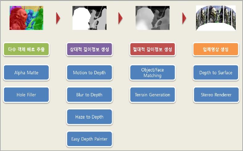
Stereoscopic conversion is largely divided in to 3 steps; object separation, formation of depth information and stereo rendering. Professor Noh’s teams focused on the optimization of each step to increase the efficiency of the conversion system.
Professor Noh’s research team first increased the separation accuracy to the degree of a single hair and created an algorithm that automatically fills in the background originally covered by the separated object.
The team succeeded in the automatic formation of depth information using the geographic or architectural characteristic and vanishing points. For the stereo rendering process, the team decreased the rendering time by reusing the rendered information of one side, rather than the traditional method of rendering the left and right images separately.
Professor Noh said that ‘although 3D TVs are becoming more and more commercialized, there are not enough programs that can be watched in 3D’ and that ‘stereoscopic conversion technology is receiving high praise in the field of graphics because it allows the easy production of 3D contents with small cost’.
2012.10.20 View 11113
3D contents using our technology
Professor Noh Jun Yong’s research team from KAIST Graduate School of Culture Technology has successfully developed a software program that improves the semiautomatic conversation rate efficiency of 3D stereoscopic images by 3 times.
This software, named ‘NAKiD’, was first presented at the renowned Computer Graphics conference/exhibition ‘Siggraph 2012’ in August and received intense interest from the participants.
The ‘NAKiD’ technology is forecasted to replace the expensive imported equipment and technology used in 3D filming.
For multi-viewpoint no-glasses 3D stereopsis, two cameras are needed to film the image. However, ‘NAKiD’ can easily convert images from a single camera into a 3D image, greatly decreasing the problems in the film production process as well as its cost.
There are 2 methods commonly used in the production of 3D stereoscopic images; filming using two cameras and the 3D conversion using computer software.
The use of two cameras requires expensive equipment and the filmed images need further processing after production. On the other hand, 3D conversion technology does not require extra devices in the production process and can also convert the existing 2D contents into 3D, a main reason why many countries are focusing on the development of stereoscopic technology.
Stereoscopic conversion is largely divided in to 3 steps; object separation, formation of depth information and stereo rendering. Professor Noh’s teams focused on the optimization of each step to increase the efficiency of the conversion system.
Professor Noh’s research team first increased the separation accuracy to the degree of a single hair and created an algorithm that automatically fills in the background originally covered by the separated object.
The team succeeded in the automatic formation of depth information using the geographic or architectural characteristic and vanishing points. For the stereo rendering process, the team decreased the rendering time by reusing the rendered information of one side, rather than the traditional method of rendering the left and right images separately.
Professor Noh said that ‘although 3D TVs are becoming more and more commercialized, there are not enough programs that can be watched in 3D’ and that ‘stereoscopic conversion technology is receiving high praise in the field of graphics because it allows the easy production of 3D contents with small cost’.
2012.10.20 View 11113 -
 DNA based semiconductor technology developed
Professor Park Hyun Gyu’s research team from the Department of Chemical and Biomolecular Engineering at KAIST has successfully implemented all logic gates using DNA, a feat that led the research to be published as the cover paper for the international nanotechnology paper "Small".
Even with the latest technology, it was impossible to create a silicon based semiconductor smaller than 10nm, but because DNA has a thickness of only 2nm, this could lead to the creation of semiconductors with groundbreaking degrees of integration.
A 2 nm semiconductor will be able to store 10,000 HD movies within a size of a postage stamp, at least 100 times more than the current 20nm semiconductors.
DNAs are comprised of 4 bases which are continually connected: Adenine (A) with Thymine (T), and Guanine (G) with Cytosine (C).
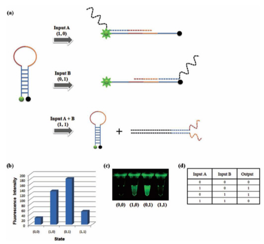
For this research, the team used the specific binding properties of DNA, which forms its helix-shape, and a circular molecular beacon that has fluorescent signaling properties under structural changes.
The research team used input signals to open and close the circular DNA, the same principle that is applied to logic gates in digital circuits.
The output signal was measured using the increase and decrease of the fluorescent signal from the molecular beacon due to the opening and closing of the circular DNA respectively.
The team overcame the limited system problems of the existing logic gates and managed to implement all 8 logic gates (AND, OR, XOR, INHIBIT, NAND, NOR, XNOR, IMPlCATION). A multilevel circuit that connects different logic gates was also tested to show its regenerative properties.
Professor Park said that “cheap bio-electric devices with high degrees of integration will be made possible by this research” and that “there will be a large difference in the field of molecular level electronic research”
Mr. Park Gi Su, a doctoral candidate and the 1st author of this research, said that “a DNA sequence of 10 bases is only 3.4nm long and 2nm thick, which can be used to effectively increase the degree of integration of electronic devices” and that “a bio computer could materialize in the near future through DNA semiconductors with accurate logic gates”.
XOR Gate: The output signal 1 comes through the open circular DNA when either input DNA A or input DNA B is present. When both inputs are not present, the flourescent signal does not come through
2012.09.27 View 10957
DNA based semiconductor technology developed
Professor Park Hyun Gyu’s research team from the Department of Chemical and Biomolecular Engineering at KAIST has successfully implemented all logic gates using DNA, a feat that led the research to be published as the cover paper for the international nanotechnology paper "Small".
Even with the latest technology, it was impossible to create a silicon based semiconductor smaller than 10nm, but because DNA has a thickness of only 2nm, this could lead to the creation of semiconductors with groundbreaking degrees of integration.
A 2 nm semiconductor will be able to store 10,000 HD movies within a size of a postage stamp, at least 100 times more than the current 20nm semiconductors.
DNAs are comprised of 4 bases which are continually connected: Adenine (A) with Thymine (T), and Guanine (G) with Cytosine (C).
For this research, the team used the specific binding properties of DNA, which forms its helix-shape, and a circular molecular beacon that has fluorescent signaling properties under structural changes.
The research team used input signals to open and close the circular DNA, the same principle that is applied to logic gates in digital circuits.
The output signal was measured using the increase and decrease of the fluorescent signal from the molecular beacon due to the opening and closing of the circular DNA respectively.
The team overcame the limited system problems of the existing logic gates and managed to implement all 8 logic gates (AND, OR, XOR, INHIBIT, NAND, NOR, XNOR, IMPlCATION). A multilevel circuit that connects different logic gates was also tested to show its regenerative properties.
Professor Park said that “cheap bio-electric devices with high degrees of integration will be made possible by this research” and that “there will be a large difference in the field of molecular level electronic research”
Mr. Park Gi Su, a doctoral candidate and the 1st author of this research, said that “a DNA sequence of 10 bases is only 3.4nm long and 2nm thick, which can be used to effectively increase the degree of integration of electronic devices” and that “a bio computer could materialize in the near future through DNA semiconductors with accurate logic gates”.
XOR Gate: The output signal 1 comes through the open circular DNA when either input DNA A or input DNA B is present. When both inputs are not present, the flourescent signal does not come through
2012.09.27 View 10957 -
Liver Damage Mechanism of Hepatitis C Proven
KAIST researchers found mechanics behind a Hepatitis C virus, thereby taking a step closer to the development of a cure for Hepatitis C.
Professor Choi Chul Hui (Department of Biological and Brain Engineering) and Professor Shin Eui Chul (Graduate School of Medical Sciences) proved, for the first time in the world, the mechanism behind liver damage of a patient with Hepatitis C.
It is anticipated that this discovery will allow for the development of a Hepatitis C cure that has no side effects and little Liver damage.
Hepatitis C is an immune response of the body to the Hepatitis C virus and causes liver irritation.
Around 170million people are infected with Hepatitis C worldwide including 1% of the Korean population. Once infected, most cases turn into chronic cases and may lead to liver cancer.
However it was impossible to infect Hepatitis C within a test tube cell environment until 2005 and up till then Chimpanzees were used to study the virus which proved to be a huge barrier to research.
The research team used cells infected with Hepatitis C virus and found out that the virus works by increasing the destruction of cells by the TNF-a protein responsible for the cell’s immune response.
In addition the protein structure of the virus that causes this reaction was successfully found.
Conventionally the Hepatitis C medication focused on the suppressing the growth of the virus and therefore had many side effects.
The experimental results allow new medication aimed at suppressing the actual mechanism of liver damage to be discovered.
The result was selected as the cover dissertation of the September Edition of the Hepatolog magazine.
2012.09.11 View 14173
-
Jellyfish removal robot developed
Professor Myung Hyun’s research team from the Department of Civil and Environmental Engineering at KAIST has developed a jellyfish removal robot named ‘JEROS’ (JEROS: Jellyfish Elimination RObotic Swarm).
With jellyfish attacks around the south-west coast of Korea becoming a serious problem, causing deaths and operational losses (around 3 billion won a year), Professor Myung’s team started the development of this unmanned automatic jellyfish removal system 3 years ago.
JEROS floats on the surface of the water using two long cylindrical bodies. Motors are attached to the bodies such that the robot can move back and forth as well as rotate on water. A camera and GPS system allows the JEROS to detect jellyfish swarm as well as plan and calculate its work path relative to its position.
The jellyfish are removed by a submerged net that sucks them up using the velocity created by the unmanned sailing. Once caught, the jellyfish are pulverized using a special propeller.
JEROS is estimated to be 3 times more economical than manual removal. Upon experimentation, it showed a removal rate of 400kg per hour at 6 knots. To reach similar effectiveness as manual net removal, which removes up to 1 ton per hour, the research team designed the robot such that 3 or more individual robots could be grouped together and controlled as one.
The research team has finished conducting removal tests in Gunsan and Masan and plan to commercialize the robot next April after improving the removal technology. JEROS technology can also be used for a wide range of purposes such as patrolling and guarding, preventing oil spills or removing floating waste. This research was funded by the Ministry of Education, Science and Technology since 2010.
2012.08.29 View 13371