Atom
-
 First Instance of Negative Effects from Terahertz-Range Electromagnetic Waves
Professor Philhan Kim
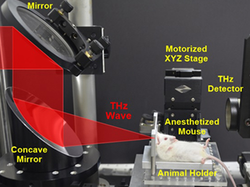
Electromagnetic waves (EM-wave) in the terahertz range were widely regarded as the “dream wavelength” due to its perceived neutrality. Its application was also wider than X-rays. However, KAIST scientists have discovered negative effects from terahertz EM-waves.
Professor Philhan Kim of KAIST’s Graduate School of Nanoscience and Technology and Dr. Young-wook Jeong of the Korea Atomic Energy Research Institute (KAERI) observed inflammation of animal skin tissue when exposed to terahertz EM-waves.
The results were published in the online edition of Optics Express (May 19, 20104).
Terahertz waves range from 0.1 to 10 terahertz and have a longer wavelength than visible or infrared light. Commonly used to see through objects like the X-ray, it was believed that the low energy of terahertz waves did not inflict any harm on the human body.
Despite being applied for security checks, next-generation wireless communications, and medical imaging technology, little research has been conducted in proving its safety and impact. Conventional research failed to predict the exact impact of terahertz waves on organic tissues as only artificially cultured cells were used.
The research team at KAERI developed a high power terahertz EM-wave generator that can be used on live organisms. A high power generator was necessary in applications such as biosensors and required up to 10 times greater power than currently used telecommunications EM-wave. Simultaneously, a KAIST research team developed a high speed, high resolution video-laser microscope that can distinguish cells within the organism.
The experiment exposed 30 minutes of terahertz EM-wave on genetically modified mice and found six times the normal number of inflammation cells in the skin tissue after six hours. It was the first instance where negative side effects of terahertz EM-wave were observed.
Professor Kim commented that “the research has set a standard for how we can use the terahertz EM-wave safely” and that “we will use this research to analyze and understand the effects of other EM-waves on organisms.”
2014.06.20 View 11387
First Instance of Negative Effects from Terahertz-Range Electromagnetic Waves
Professor Philhan Kim
Electromagnetic waves (EM-wave) in the terahertz range were widely regarded as the “dream wavelength” due to its perceived neutrality. Its application was also wider than X-rays. However, KAIST scientists have discovered negative effects from terahertz EM-waves.
Professor Philhan Kim of KAIST’s Graduate School of Nanoscience and Technology and Dr. Young-wook Jeong of the Korea Atomic Energy Research Institute (KAERI) observed inflammation of animal skin tissue when exposed to terahertz EM-waves.
The results were published in the online edition of Optics Express (May 19, 20104).
Terahertz waves range from 0.1 to 10 terahertz and have a longer wavelength than visible or infrared light. Commonly used to see through objects like the X-ray, it was believed that the low energy of terahertz waves did not inflict any harm on the human body.
Despite being applied for security checks, next-generation wireless communications, and medical imaging technology, little research has been conducted in proving its safety and impact. Conventional research failed to predict the exact impact of terahertz waves on organic tissues as only artificially cultured cells were used.
The research team at KAERI developed a high power terahertz EM-wave generator that can be used on live organisms. A high power generator was necessary in applications such as biosensors and required up to 10 times greater power than currently used telecommunications EM-wave. Simultaneously, a KAIST research team developed a high speed, high resolution video-laser microscope that can distinguish cells within the organism.
The experiment exposed 30 minutes of terahertz EM-wave on genetically modified mice and found six times the normal number of inflammation cells in the skin tissue after six hours. It was the first instance where negative side effects of terahertz EM-wave were observed.
Professor Kim commented that “the research has set a standard for how we can use the terahertz EM-wave safely” and that “we will use this research to analyze and understand the effects of other EM-waves on organisms.”
2014.06.20 View 11387 -
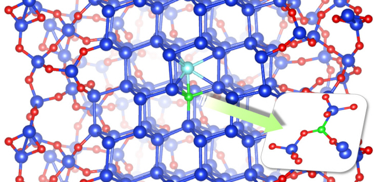
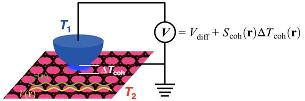 An Electron Cloud Distribution Observed by the Scanning Seebeck Microscope
All matters are made of small particles, namely atoms. An atom is composed of a heavy nucleus and cloud-like, extremely light electrons.
Korean researchers developed an electron microscopy technique that enables the accurate observation of an electron cloud distribution at room-temperature. The achievement is comparable to the invention of the quantum tunneling microscopy technique developed 33 years ago.
Professor Yong-Hyun Kim of the Graduate School of Nanoscience and Technology at KAIST and Dr. Ho-Gi Yeo of the Korea Research Institute of Standards and Science (KRISS) developed the Scanning Seebeck Microscope (SSM). The SSM renders clear images of atoms, as well as an electron cloud distribution. This was achieved by creating a voltage difference via a temperature gradient.
The development was introduced in the online edition of Physical Review Letters (April 2014), a prestigious journal published by the American Institute of Physics.
The SSM is expected to be economically competitive as it gives high resolution images at an atomic scale even for graphene and semiconductors, both at room temperature. In addition, if the SSM is applied to thermoelectric material research, it will contribute to the development of high-efficiency thermoelectric materials.
Through numerous hypotheses and experiments, scientists now believe that there exists an electron cloud surrounding a nucleus. IBM's Scanning Tunneling Microscope (STM) was the first to observe the electron cloud and has remained as the only technique to this day. The developers of IBM microscope, Dr. Gerd Binnig and Dr. Heinrich Rohrer, were awarded the 1986 Nobel Prize in Physics.
There still remains a downside to the STM technique, however: it required high precision and extreme low temperature and vibration. The application of voltage also affects the electron cloud, resulting in a distorted image.
The KAIST research team adopted a different approach by using the Seebeck effect which refers to the voltage generation due to a temperature gradient between two materials.
The team placed an observation sample (graphene) at room temperature (37~57℃) and detected its voltage generation. This technique made it possible to observe an electron cloud at room temperature.
Furthermore, the research team investigated the theoretical quantum mechanics behind the electron cloud using the observation gained through the Seebeck effect and also obtained by simulation capability to analyze the experimental results.
The research was a joint research project between KAIST Professor Yong-Hyun Kim and KRISS researcher Dr. Ho-Gi Yeo. Eui-Seop Lee, a Ph.D. candidate of KAIST, and KRISS researcher Dr. Sang-Hui Cho also participated. The Ministry of Science, ICT, and Future Planning, the Global Frontier Initiative, and the Disruptive Convergent Technology Development Initiative funded the project in Korea.
Picture 1: Schematic Diagram of the Scanning Seebeck Microscope (SSM)
Picture 2: Electron cloud distribution observed by SSM at room temperature
Picture 3: Professor Yong-Hyun Kim
2014.04.04 View 17585
An Electron Cloud Distribution Observed by the Scanning Seebeck Microscope
All matters are made of small particles, namely atoms. An atom is composed of a heavy nucleus and cloud-like, extremely light electrons.
Korean researchers developed an electron microscopy technique that enables the accurate observation of an electron cloud distribution at room-temperature. The achievement is comparable to the invention of the quantum tunneling microscopy technique developed 33 years ago.
Professor Yong-Hyun Kim of the Graduate School of Nanoscience and Technology at KAIST and Dr. Ho-Gi Yeo of the Korea Research Institute of Standards and Science (KRISS) developed the Scanning Seebeck Microscope (SSM). The SSM renders clear images of atoms, as well as an electron cloud distribution. This was achieved by creating a voltage difference via a temperature gradient.
The development was introduced in the online edition of Physical Review Letters (April 2014), a prestigious journal published by the American Institute of Physics.
The SSM is expected to be economically competitive as it gives high resolution images at an atomic scale even for graphene and semiconductors, both at room temperature. In addition, if the SSM is applied to thermoelectric material research, it will contribute to the development of high-efficiency thermoelectric materials.
Through numerous hypotheses and experiments, scientists now believe that there exists an electron cloud surrounding a nucleus. IBM's Scanning Tunneling Microscope (STM) was the first to observe the electron cloud and has remained as the only technique to this day. The developers of IBM microscope, Dr. Gerd Binnig and Dr. Heinrich Rohrer, were awarded the 1986 Nobel Prize in Physics.
There still remains a downside to the STM technique, however: it required high precision and extreme low temperature and vibration. The application of voltage also affects the electron cloud, resulting in a distorted image.
The KAIST research team adopted a different approach by using the Seebeck effect which refers to the voltage generation due to a temperature gradient between two materials.
The team placed an observation sample (graphene) at room temperature (37~57℃) and detected its voltage generation. This technique made it possible to observe an electron cloud at room temperature.
Furthermore, the research team investigated the theoretical quantum mechanics behind the electron cloud using the observation gained through the Seebeck effect and also obtained by simulation capability to analyze the experimental results.
The research was a joint research project between KAIST Professor Yong-Hyun Kim and KRISS researcher Dr. Ho-Gi Yeo. Eui-Seop Lee, a Ph.D. candidate of KAIST, and KRISS researcher Dr. Sang-Hui Cho also participated. The Ministry of Science, ICT, and Future Planning, the Global Frontier Initiative, and the Disruptive Convergent Technology Development Initiative funded the project in Korea.
Picture 1: Schematic Diagram of the Scanning Seebeck Microscope (SSM)
Picture 2: Electron cloud distribution observed by SSM at room temperature
Picture 3: Professor Yong-Hyun Kim
2014.04.04 View 17585 -
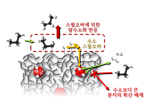 Spillover Phenomenon Identified Using Model Catalyst System
Researchers at KAIST have identified spillover phenomenon, which has remained controversial since its discovery in the early 1960s.
KAIST Department of Chemical and Biomolecular Engineering’s Professor Min-Gi Choi and his team has explained the "spillover phenomenon," using their own model catalyst system where platinum is selectively located within the amorphous aluminosilicate.
The research results were published on the 25th February online edition of Nature Communications.
Spillover refers to a phenomenon that occurs when hydrogen atoms that have been activated on the surface of metals, such as platinum, move to the surface of the catalyst. It was predicted that this phenomenon can be used to design a catalyst with high activity and stability, and thus has been actively studied over the last 50 years.
However, many cases of the known catalysts involved competing reactions on the exposed metal surface, which made it impossible to directly identify the presence and formation mechanism of spillover.
The catalysts developed by the researchers at KAIST used platinum nanoparticles covered with aluminosilicate. This only allowed the hydrogen molecules to pass through and has effectively blocked the competing reactions, enabling the research team to study the spillover phenomenon.
Through various catalyst structure and reactivity analysis, as well as computer modeling, the team has discovered that Brönsted acid sites present on the aluminosilicate plays a crucial role in spillover phenomenon.
In addition, the spillover-based hydrogenation catalyst proposed by the research team showed very high hydrogenation and dehydrogenation activity. The ability of the catalyst to significantly inhibit unwanted hydrogenolysis reaction during the petrochemical processes also suggested a large industrial potential.
Professor Min-Gi Choi said, “This particular catalyst, which can trigger the reaction only by spillover phenomenon, can be properly designed to exceed the capacity of the conventional metal catalysts. The future goal is to make a catalyst with much higher activity and selectivity.”
The research was conducted through funds subsidized by SK Innovation and Ministry of Science, ICT and Future Planning.
The senior research fellow of SK Innovation Seung-Hun Oh said, “SK Innovation will continue to develop a new commercial catalyst based on the technology from this research.”
Juh-Wan Lim and Hye-Yeong Shin led the research as joint first authors under supervision of Professor Min-Gi Choi and computer modeling works were conducted by KAIST EEWS (environment, energy, water, and sustainability) graduate school’s Professor Hyeong-Jun Kim.
2014.03.03 View 12150
Spillover Phenomenon Identified Using Model Catalyst System
Researchers at KAIST have identified spillover phenomenon, which has remained controversial since its discovery in the early 1960s.
KAIST Department of Chemical and Biomolecular Engineering’s Professor Min-Gi Choi and his team has explained the "spillover phenomenon," using their own model catalyst system where platinum is selectively located within the amorphous aluminosilicate.
The research results were published on the 25th February online edition of Nature Communications.
Spillover refers to a phenomenon that occurs when hydrogen atoms that have been activated on the surface of metals, such as platinum, move to the surface of the catalyst. It was predicted that this phenomenon can be used to design a catalyst with high activity and stability, and thus has been actively studied over the last 50 years.
However, many cases of the known catalysts involved competing reactions on the exposed metal surface, which made it impossible to directly identify the presence and formation mechanism of spillover.
The catalysts developed by the researchers at KAIST used platinum nanoparticles covered with aluminosilicate. This only allowed the hydrogen molecules to pass through and has effectively blocked the competing reactions, enabling the research team to study the spillover phenomenon.
Through various catalyst structure and reactivity analysis, as well as computer modeling, the team has discovered that Brönsted acid sites present on the aluminosilicate plays a crucial role in spillover phenomenon.
In addition, the spillover-based hydrogenation catalyst proposed by the research team showed very high hydrogenation and dehydrogenation activity. The ability of the catalyst to significantly inhibit unwanted hydrogenolysis reaction during the petrochemical processes also suggested a large industrial potential.
Professor Min-Gi Choi said, “This particular catalyst, which can trigger the reaction only by spillover phenomenon, can be properly designed to exceed the capacity of the conventional metal catalysts. The future goal is to make a catalyst with much higher activity and selectivity.”
The research was conducted through funds subsidized by SK Innovation and Ministry of Science, ICT and Future Planning.
The senior research fellow of SK Innovation Seung-Hun Oh said, “SK Innovation will continue to develop a new commercial catalyst based on the technology from this research.”
Juh-Wan Lim and Hye-Yeong Shin led the research as joint first authors under supervision of Professor Min-Gi Choi and computer modeling works were conducted by KAIST EEWS (environment, energy, water, and sustainability) graduate school’s Professor Hyeong-Jun Kim.
2014.03.03 View 12150 -
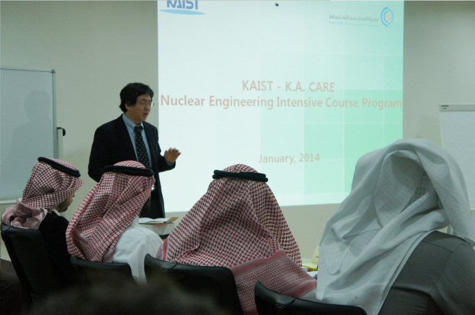 KAIST-Saudi Nuclear Workforce Training
Nuclear Engineering Intensive Course Program Held in Saudi Arabia from January 5th to 23rd
KUSTAR (The Khalifa University of Science and Technology Studies)-KAIST Institute of Education began its Nuclear Engineering Intensive Course Program on 5th January with researchers from K.A.CARE (King Abdullah City for Atomic and Renewable Energy) of Riyadh, Saudi Arabia.
This program, which was lasted until 23rd January, provided education to students on the basic technologies in the field of nuclear power.
The course involves a wide range of lectures, such as basic nuclear physics, applications using radiation, nuclear reactor design and safety, as well as nuclear power engineering.
In order to utilize the nuclear power and renewable energy, K.A.CARE was established in April 2010. The institution is also involved in the construction of nuclear infrastructure, including the site investigations, the establishment of regulatory bodies and state-owned nuclear companies, along with the newly launched workforce-training program.
The Director of the KUSTAR-KAIST Education Research Institute, Professor Soong-Heung Jang said, “This program is the beginning of long-term cooperation with Saudi Arabia. Our experience can be the basis for the construction of an extensive training program that involves many areas of nuclear engineering field.”
KAIST has been working in close cooperation with various institutions around the world, which also includes the establishment of KUSTAR-KAIST Institute of Education and Research in July 2010. KAIST is also actively cooperating with UAE Khalifa University in Middle East, sharing faculty, holding joint research programs and exchanging students.
2014.02.03 View 13327
KAIST-Saudi Nuclear Workforce Training
Nuclear Engineering Intensive Course Program Held in Saudi Arabia from January 5th to 23rd
KUSTAR (The Khalifa University of Science and Technology Studies)-KAIST Institute of Education began its Nuclear Engineering Intensive Course Program on 5th January with researchers from K.A.CARE (King Abdullah City for Atomic and Renewable Energy) of Riyadh, Saudi Arabia.
This program, which was lasted until 23rd January, provided education to students on the basic technologies in the field of nuclear power.
The course involves a wide range of lectures, such as basic nuclear physics, applications using radiation, nuclear reactor design and safety, as well as nuclear power engineering.
In order to utilize the nuclear power and renewable energy, K.A.CARE was established in April 2010. The institution is also involved in the construction of nuclear infrastructure, including the site investigations, the establishment of regulatory bodies and state-owned nuclear companies, along with the newly launched workforce-training program.
The Director of the KUSTAR-KAIST Education Research Institute, Professor Soong-Heung Jang said, “This program is the beginning of long-term cooperation with Saudi Arabia. Our experience can be the basis for the construction of an extensive training program that involves many areas of nuclear engineering field.”
KAIST has been working in close cooperation with various institutions around the world, which also includes the establishment of KUSTAR-KAIST Institute of Education and Research in July 2010. KAIST is also actively cooperating with UAE Khalifa University in Middle East, sharing faculty, holding joint research programs and exchanging students.
2014.02.03 View 13327 -
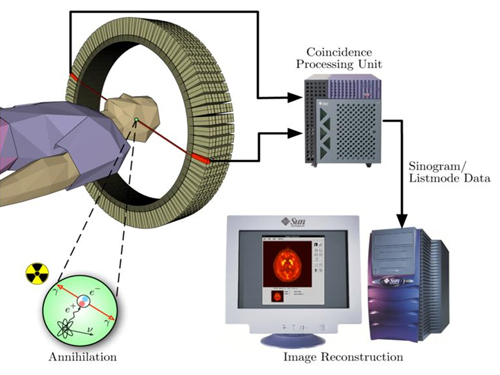 The key to Alzheimer disease, PET-MRI made in Korea
Professor Kyu-Sung Cho
- Simultaneous PET-MRI imaging system commercialization technology developed purely from domestic technology - - Inspiring achievement by KAIST, National NanoFab Center, Sogang University, Seoul National University Hospital –
Hopes are high for the potential of producing domestic products in the field of state-of-the-art medical imaging equipment that used to rely on imported products.
The joint research team (KAIST, Sogang University and Seoul National University) with KAIST Department of Nuclear and Quantum Engineering Professor Kyu-Sung Cho in charge, together with National Nanofab Institution (NNFC; Director Jae-Young Lee), has developed PET-MRI simultaneous imaging system with domestic technology only. The team successfully acquired brain images of 3 volunteers with the newly developed system.
PET-MRI is integrated state-of-the-art medical imaging equipment that combines the advantages of Magnetic Resonance Imaging (MRI) that shows anatomical images of the body and Position Emission Tomography (PET) that analyses cell activity and metabolism. Since the anatomical information and functional information can be seen simultaneously, the device can be used to diagnose early onset Alzheimer’s disease and is essential in biological science research, such as new medicine development.
The existing equipment used to take MRI and PET images separately due to the strong magnetic field generated by MRI and combine the images. Hence, it was time consuming and error-prone due to patient’s movement. There was a need to develop PET that functions within a magnetic field to create a simultaneous imaging system.
The newly developed integral PET-MRI has 3 technical characteristics: 1. PET detector without magnetic interference, 2. PET-MRI integration system, 3.PET-MRI imaging processing.
The PET detector is the most important factor and accounts for half the cost of the whole system. KAIST Professor Cho and NNFC Doctor Woo-Suk Seol’s team successfully developed the Silicon Photomultiplier (amplifies light coming into the radiation detector) that can be used in strong magnetic fields. The developed sensor has a global competitive edge since it optimises semiconductor processing to yield over 95% productivity and around 10% gamma radiation energy resolving power.
Sogang University Department and Electrical Engineering Professor Yong Choi developed cutting edge PET system using a new concept of electric charge signal transmission method and imaging location distinction circuit. The creativity and excellence of the research findings were recognised and hence published on the cover of Medical Physics in June.
Seoul National University Hospital Department of Nuclear Medicine Professor Jae-Sung Lee developed the Silicon Photomultiplier sensor based PET imaging reconstitution programme, MRI imaging based PET imaging revision technology and PET-MRI imaging integration software.
Furthermore, KAIST Department of Electrical Engineering Professor Hyun-Wook Park was responsible for the development of RF Shielding technology that enables simultaneous installation of PET and MRI and using this technology, he developed a head coil for the brain that can be connected to PET for installation.
Based on the technology describe above, the joint research team successfully developed PET-MRI system for brains and acquired PET-MRI integrated brain images from 3 volunteers last June.
In particular, this system has the distinct feature of a detachable PET module and MRI head coil to the existing whole body MRI, so that PET-MRI simultaneous imaging is possible with low installation cost.
Professor Cho said, “We have prepared the foundation of domestic commercial PET and the system has a competitive edge in the global market of PET-MRI system technology.” He continued, “It can reduce the cost of the increasing brain related disease diagnosis, including Alzheimer’s, dramatically.”
Funded by Ministry of Trade, Industry and Energy as an Industrial Foundation Technology Development Project (98 billion won in 7 years), the research applied for over 20 patents and 20 CSI theses.
Figure 1.Brain phantom images from developed PET-MRI system
Figure 2. Brain images from developed PET-MRI system
Figure 3. Domestic PET-MRI clinical trial
Figure 4. Head RF coil and PET detector inserted in MRI
Figure 5. Insertion type PET detector module
Figure 6. Silicon Photomultiplier sensor (Left) and flash crystal block (right)
Figure7. Silicon Photomultiplier sensor
Figure 8. PET detection principle
2013.11.28 View 16197
The key to Alzheimer disease, PET-MRI made in Korea
Professor Kyu-Sung Cho
- Simultaneous PET-MRI imaging system commercialization technology developed purely from domestic technology - - Inspiring achievement by KAIST, National NanoFab Center, Sogang University, Seoul National University Hospital –
Hopes are high for the potential of producing domestic products in the field of state-of-the-art medical imaging equipment that used to rely on imported products.
The joint research team (KAIST, Sogang University and Seoul National University) with KAIST Department of Nuclear and Quantum Engineering Professor Kyu-Sung Cho in charge, together with National Nanofab Institution (NNFC; Director Jae-Young Lee), has developed PET-MRI simultaneous imaging system with domestic technology only. The team successfully acquired brain images of 3 volunteers with the newly developed system.
PET-MRI is integrated state-of-the-art medical imaging equipment that combines the advantages of Magnetic Resonance Imaging (MRI) that shows anatomical images of the body and Position Emission Tomography (PET) that analyses cell activity and metabolism. Since the anatomical information and functional information can be seen simultaneously, the device can be used to diagnose early onset Alzheimer’s disease and is essential in biological science research, such as new medicine development.
The existing equipment used to take MRI and PET images separately due to the strong magnetic field generated by MRI and combine the images. Hence, it was time consuming and error-prone due to patient’s movement. There was a need to develop PET that functions within a magnetic field to create a simultaneous imaging system.
The newly developed integral PET-MRI has 3 technical characteristics: 1. PET detector without magnetic interference, 2. PET-MRI integration system, 3.PET-MRI imaging processing.
The PET detector is the most important factor and accounts for half the cost of the whole system. KAIST Professor Cho and NNFC Doctor Woo-Suk Seol’s team successfully developed the Silicon Photomultiplier (amplifies light coming into the radiation detector) that can be used in strong magnetic fields. The developed sensor has a global competitive edge since it optimises semiconductor processing to yield over 95% productivity and around 10% gamma radiation energy resolving power.
Sogang University Department and Electrical Engineering Professor Yong Choi developed cutting edge PET system using a new concept of electric charge signal transmission method and imaging location distinction circuit. The creativity and excellence of the research findings were recognised and hence published on the cover of Medical Physics in June.
Seoul National University Hospital Department of Nuclear Medicine Professor Jae-Sung Lee developed the Silicon Photomultiplier sensor based PET imaging reconstitution programme, MRI imaging based PET imaging revision technology and PET-MRI imaging integration software.
Furthermore, KAIST Department of Electrical Engineering Professor Hyun-Wook Park was responsible for the development of RF Shielding technology that enables simultaneous installation of PET and MRI and using this technology, he developed a head coil for the brain that can be connected to PET for installation.
Based on the technology describe above, the joint research team successfully developed PET-MRI system for brains and acquired PET-MRI integrated brain images from 3 volunteers last June.
In particular, this system has the distinct feature of a detachable PET module and MRI head coil to the existing whole body MRI, so that PET-MRI simultaneous imaging is possible with low installation cost.
Professor Cho said, “We have prepared the foundation of domestic commercial PET and the system has a competitive edge in the global market of PET-MRI system technology.” He continued, “It can reduce the cost of the increasing brain related disease diagnosis, including Alzheimer’s, dramatically.”
Funded by Ministry of Trade, Industry and Energy as an Industrial Foundation Technology Development Project (98 billion won in 7 years), the research applied for over 20 patents and 20 CSI theses.
Figure 1.Brain phantom images from developed PET-MRI system
Figure 2. Brain images from developed PET-MRI system
Figure 3. Domestic PET-MRI clinical trial
Figure 4. Head RF coil and PET detector inserted in MRI
Figure 5. Insertion type PET detector module
Figure 6. Silicon Photomultiplier sensor (Left) and flash crystal block (right)
Figure7. Silicon Photomultiplier sensor
Figure 8. PET detection principle
2013.11.28 View 16197 -
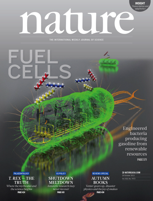 KAIST announced a novel technology to produce gasoline by a metabolically engineered microorganism
A major scientific breakthrough in the development of renewable energy sources and other important chemicals; The research team succeeded in producing 580 mg of gasoline per liter of cultured broth by converting in vivo generated fatty acids
For many decades, we have been relying on fossil resources to produce liquid fuels such as gasoline, diesel, and many industrial and consumer chemicals for daily use. However, increasing strains on natural resources as well as environmental issues including global warming have triggered a strong interest in developing sustainable ways to obtain fuels and chemicals.
Gasoline, the petroleum-derived product that is most widely used as a fuel for transportation, is a mixture of hydrocarbons, additives, and blending agents. The hydrocarbons, called alkanes, consist only of carbon and hydrogen atoms. Gasoline has a combination of straight-chain and branched-chain alkanes (hydrocarbons) consisted of 4-12 carbon atoms linked by direct carbon-carbon bonds.
Previously, through metabolic engineering of Escherichia coli (E. coli), there have been a few research results on the production of long-chain alkanes, which consist of 13-17 carbon atoms, suitable for replacing diesel. However, there has been no report on the microbial production of short-chain alkanes, a possible substitute for gasoline.
In the paper (entitled "Microbial Production of Short-chain Alkanes") published online in Nature on September 29, a Korean research team led by Distinguished Professor Sang Yup Lee of the Department of Chemical and Biomolecular Engineering at the Korea Advanced Institute of Science and Technology (KAIST) reported, for the first time, the development of a novel strategy for microbial gasoline production through metabolic engineering of E. coli.
The research team engineered the fatty acid metabolism to provide the fatty acid derivatives that are shorter than normal intracellular fatty acid metabolites, and introduced a novel synthetic pathway for the biosynthesis of short-chain alkanes. This allowed the development of platform E. coli strain capable of producing gasoline for the first time. Furthermore, this platform strain, if desired, can be modified to produce other products such as short-chain fatty esters and short-chain fatty alcohols.
In this paper, the Korean researchers described detailed strategies for 1) screening of enzymes associated with the production of fatty acids, 2) engineering of enzymes and fatty acid biosynthetic pathways to concentrate carbon flux towards the short-chain fatty acid production, and 3) converting short-chain fatty acids to their corresponding alkanes (gasoline) by introducing a novel synthetic pathway and optimization of culture conditions. Furthermore, the research team showed the possibility of producing fatty esters and alcohols by introducing responsible enzymes into the same platform strain.
Professor Sang Yup Lee said, "It is only the beginning of the work towards sustainable production of gasoline. The titer is rather low due to the low metabolic flux towards the formation of short-chain fatty acids and their derivatives. We are currently working on increasing the titer, yield and productivity of bio-gasoline. Nonetheless, we are pleased to report, for the first time, the production of gasoline through the metabolic engineering of E. coli, which we hope will serve as a basis for the metabolic engineering of microorganisms to produce fuels and chemicals from renewable resources."
This research was supported by the Advanced Biomass Research and Development Center of Korea (ABC-2010-0029799) through the Global Frontier Research Program of the Ministry of Science, ICT and Future Planning (MSIP) through the National Research Foundation (NRF), Republic of Korea. Systems metabolic engineering work was supported by the Technology Development Program to Solve Climate Changes on Systems Metabolic Engineering for Biorefineries (NRF-2012-C1AAA001-2012M1A2A2026556) by MSIP through NRF.
Short-Chain Alkanes Generated from Renewable Biomass
This diagram shows the metabolic engineering of Escherichia coli for the production of short-chain alkanes (gasoline) from renewable biomass.
Nature Cover Page (September 29th, 2013)
2013.11.04 View 14196
KAIST announced a novel technology to produce gasoline by a metabolically engineered microorganism
A major scientific breakthrough in the development of renewable energy sources and other important chemicals; The research team succeeded in producing 580 mg of gasoline per liter of cultured broth by converting in vivo generated fatty acids
For many decades, we have been relying on fossil resources to produce liquid fuels such as gasoline, diesel, and many industrial and consumer chemicals for daily use. However, increasing strains on natural resources as well as environmental issues including global warming have triggered a strong interest in developing sustainable ways to obtain fuels and chemicals.
Gasoline, the petroleum-derived product that is most widely used as a fuel for transportation, is a mixture of hydrocarbons, additives, and blending agents. The hydrocarbons, called alkanes, consist only of carbon and hydrogen atoms. Gasoline has a combination of straight-chain and branched-chain alkanes (hydrocarbons) consisted of 4-12 carbon atoms linked by direct carbon-carbon bonds.
Previously, through metabolic engineering of Escherichia coli (E. coli), there have been a few research results on the production of long-chain alkanes, which consist of 13-17 carbon atoms, suitable for replacing diesel. However, there has been no report on the microbial production of short-chain alkanes, a possible substitute for gasoline.
In the paper (entitled "Microbial Production of Short-chain Alkanes") published online in Nature on September 29, a Korean research team led by Distinguished Professor Sang Yup Lee of the Department of Chemical and Biomolecular Engineering at the Korea Advanced Institute of Science and Technology (KAIST) reported, for the first time, the development of a novel strategy for microbial gasoline production through metabolic engineering of E. coli.
The research team engineered the fatty acid metabolism to provide the fatty acid derivatives that are shorter than normal intracellular fatty acid metabolites, and introduced a novel synthetic pathway for the biosynthesis of short-chain alkanes. This allowed the development of platform E. coli strain capable of producing gasoline for the first time. Furthermore, this platform strain, if desired, can be modified to produce other products such as short-chain fatty esters and short-chain fatty alcohols.
In this paper, the Korean researchers described detailed strategies for 1) screening of enzymes associated with the production of fatty acids, 2) engineering of enzymes and fatty acid biosynthetic pathways to concentrate carbon flux towards the short-chain fatty acid production, and 3) converting short-chain fatty acids to their corresponding alkanes (gasoline) by introducing a novel synthetic pathway and optimization of culture conditions. Furthermore, the research team showed the possibility of producing fatty esters and alcohols by introducing responsible enzymes into the same platform strain.
Professor Sang Yup Lee said, "It is only the beginning of the work towards sustainable production of gasoline. The titer is rather low due to the low metabolic flux towards the formation of short-chain fatty acids and their derivatives. We are currently working on increasing the titer, yield and productivity of bio-gasoline. Nonetheless, we are pleased to report, for the first time, the production of gasoline through the metabolic engineering of E. coli, which we hope will serve as a basis for the metabolic engineering of microorganisms to produce fuels and chemicals from renewable resources."
This research was supported by the Advanced Biomass Research and Development Center of Korea (ABC-2010-0029799) through the Global Frontier Research Program of the Ministry of Science, ICT and Future Planning (MSIP) through the National Research Foundation (NRF), Republic of Korea. Systems metabolic engineering work was supported by the Technology Development Program to Solve Climate Changes on Systems Metabolic Engineering for Biorefineries (NRF-2012-C1AAA001-2012M1A2A2026556) by MSIP through NRF.
Short-Chain Alkanes Generated from Renewable Biomass
This diagram shows the metabolic engineering of Escherichia coli for the production of short-chain alkanes (gasoline) from renewable biomass.
Nature Cover Page (September 29th, 2013)
2013.11.04 View 14196 -
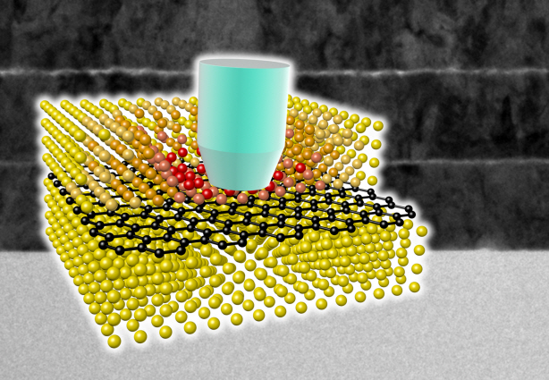 Ultra-High Strength Metamaterial Developed Using Graphene
New metamaterial has been developed, exhibiting hundreds of times greater strength than pure metals.
Professor Seung Min, Han and Yoo Sung, Jeong (Graduate School of Energy, Environment, Water, and Sustainability (EEWS)) and Professor Seok Woo, Jeon (Department of Material Science and Engineering) have developed a composite nanomaterial. The nanomaterial consists of graphene inserted in copper and nickel and exhibits strengths 500 times and 180 times, respectively, greater than that of pure metals. The result of the research was published on the July 2nd online edition in Nature Communications journal.
Graphene displays strengths 200 times greater than that of steel, is stretchable, and is flexible. The U.S. Army Armaments Research, Development and Engineering Center developed a graphene-metal nanomaterial but failed to drastically improve the strength of the material.
To maximize the strength increased by the addition of graphene, the KAIST research team created a layered structure of metal and graphene. Using CVD (Chemical Vapor Deposition), the team grew a single layer of graphene on a metal deposited substrate and then deposited another metal layer. They repeated this process to produce a metal-graphene multilayer composite material, utilizing a single layer of graphene. Micro-compression tests within Transmission Electronic Microscope and Molecular Dynamics simulations effectively showed the strength enhancing effect and the dislocation movement in grain boundaries of graphene on an atomic level.
The mechanical characteristics of the graphene layer within the metal-graphene composite material successfully blocked the dislocations and cracks from external damage from traveling inwards. Therefore the composite material displayed strength beyond conventional metal-metal multilayer materials. The copper-graphene multilayer material with an interplanar distance of 70nm exhibited 500 times greater (1.5GPa) strength than pure copper. Nickel-graphene multilayer material with an interplanar distance of 100nm showed 180 times greater (4.0GPa) strength than pure nickel.
It was found that there is a clear relationship between the interplanar distance and the strength of the multilayer material. A smaller interplanar distance made the dislocation movement more difficult and therefore increased the strength of the material. Professor Han, who led the research, commented, “the result is astounding as 0.00004% in weight of graphene increased the strength of the materials by hundreds of times” and “improvements based on this success, especially mass production with roll-to-roll process or metal sintering process in the production of ultra-high strength, lightweight parts for automobile and spacecraft, may become possible.” In addition, Professor Han mentioned that “the new material can be applied to coating materials for nuclear reactor construction or other structural materials requiring high reliability.”
The research project received support from National Research Foundation, Global Frontier Program, KAIST EEWS-KINC Program and KISTI Supercomputer and was a collaborative effort with KISTI (Korea Institute of Science and Technology Information), KBSI (Korea Basic Science Institute), Stanford University, and Columbia University.
A schematic diagram shows the structure of metal-graphene multi-layers. The metal-graphene multi-layered composite materials, containing a single-layered graphene, block the dislocation movement of graphene layers, resulting in a greater strength in the materials.
2013.08.23 View 19478
Ultra-High Strength Metamaterial Developed Using Graphene
New metamaterial has been developed, exhibiting hundreds of times greater strength than pure metals.
Professor Seung Min, Han and Yoo Sung, Jeong (Graduate School of Energy, Environment, Water, and Sustainability (EEWS)) and Professor Seok Woo, Jeon (Department of Material Science and Engineering) have developed a composite nanomaterial. The nanomaterial consists of graphene inserted in copper and nickel and exhibits strengths 500 times and 180 times, respectively, greater than that of pure metals. The result of the research was published on the July 2nd online edition in Nature Communications journal.
Graphene displays strengths 200 times greater than that of steel, is stretchable, and is flexible. The U.S. Army Armaments Research, Development and Engineering Center developed a graphene-metal nanomaterial but failed to drastically improve the strength of the material.
To maximize the strength increased by the addition of graphene, the KAIST research team created a layered structure of metal and graphene. Using CVD (Chemical Vapor Deposition), the team grew a single layer of graphene on a metal deposited substrate and then deposited another metal layer. They repeated this process to produce a metal-graphene multilayer composite material, utilizing a single layer of graphene. Micro-compression tests within Transmission Electronic Microscope and Molecular Dynamics simulations effectively showed the strength enhancing effect and the dislocation movement in grain boundaries of graphene on an atomic level.
The mechanical characteristics of the graphene layer within the metal-graphene composite material successfully blocked the dislocations and cracks from external damage from traveling inwards. Therefore the composite material displayed strength beyond conventional metal-metal multilayer materials. The copper-graphene multilayer material with an interplanar distance of 70nm exhibited 500 times greater (1.5GPa) strength than pure copper. Nickel-graphene multilayer material with an interplanar distance of 100nm showed 180 times greater (4.0GPa) strength than pure nickel.
It was found that there is a clear relationship between the interplanar distance and the strength of the multilayer material. A smaller interplanar distance made the dislocation movement more difficult and therefore increased the strength of the material. Professor Han, who led the research, commented, “the result is astounding as 0.00004% in weight of graphene increased the strength of the materials by hundreds of times” and “improvements based on this success, especially mass production with roll-to-roll process or metal sintering process in the production of ultra-high strength, lightweight parts for automobile and spacecraft, may become possible.” In addition, Professor Han mentioned that “the new material can be applied to coating materials for nuclear reactor construction or other structural materials requiring high reliability.”
The research project received support from National Research Foundation, Global Frontier Program, KAIST EEWS-KINC Program and KISTI Supercomputer and was a collaborative effort with KISTI (Korea Institute of Science and Technology Information), KBSI (Korea Basic Science Institute), Stanford University, and Columbia University.
A schematic diagram shows the structure of metal-graphene multi-layers. The metal-graphene multi-layered composite materials, containing a single-layered graphene, block the dislocation movement of graphene layers, resulting in a greater strength in the materials.
2013.08.23 View 19478 -
 Short Wavelength, Ultra-High Speed Quantum Light Source based on Quantum Dot Developed
Professor Yong Hoon, Cho (Department of Physics) and his research team synthesized an obelisk nanostructure and successfully formed a single semiconductor quantum exhibiting high reliability to realize an ultra-high speed, highly efficient, release of quantum dots.
The result of the research effort was published in the July 5th online edition of Scientific Reports published by Nature.
Semiconductor Quantum Dots restrict electrons within a cubic boundary of few nanometers thereby exhibiting similar properties to an atom with discontinuous energy levels. Exploitation of this characteristic makes possible the development of quantum light source, critical for next generation quantum information communication and quantum encryption.
High operational temperatures, stability, rapid photon release, electric current capability, and other advantages are reasons why semiconductor quantum dots are regarded as next generation core technology.
However conventional, spontaneously formed quantum dots are densely packed in a planar structure rendering the analysis of a single quantum dot difficult and result in the poor efficiency of photon release. In addition, the internal electromagnetic effect which is caused by inter-planar stress results in low internal quantum efficiency due to the difficulty in electron-hole recombination.
Professor Cho’s research team synthesized an obelisk shaped nanostructure using nitrides that emit short wavelengths of light. The activation layer was grown on the tip of the nanostructure and the team succeeded in placing a single quantum dot on the nano-tip. The team was therefore able to confirm the ultra-high speed single photon characteristics which occur at low energy levels.
Use of unique nanostructures makes synthesis of single atomic structures without processes like patterning while enabling the release of light emitted by the quantum dot.
Using this unique method the team showed the increase in internal quantum efficiency. The electromagnetic forces apparent in thin films no longer affects the quantum dot greatly due to the obelisk structure’s reduced inter planar stress.
The newly developed quantum light source emits visible light (400nm range) and not the conventional infrared light. This characteristic makes possible it use in communication in free space and enables use of highly efficient, visible range photon detector.
Professor Cho commented that “the developed method makes quantum dot growth much easier making single photon synthesis much faster to contribute to the development of practical quantum light source.” And that “the characteristics of the obelisk nanostructure enable the easy detachment from and attachment to other substrates enabling its use in producing single chip quantum light source.”
The research was conducted under the supervision of Professor Cho. The researchers werey Jae Hyung, Kim (first author) and Yong Ho, Ko (second author), both Ph.D. candidates at KAIST. The Ministry of Science, ICT and Future Planning, the National Research Foundation, and WCU Program provided support to the research effort.
2013.08.23 View 9856
Short Wavelength, Ultra-High Speed Quantum Light Source based on Quantum Dot Developed
Professor Yong Hoon, Cho (Department of Physics) and his research team synthesized an obelisk nanostructure and successfully formed a single semiconductor quantum exhibiting high reliability to realize an ultra-high speed, highly efficient, release of quantum dots.
The result of the research effort was published in the July 5th online edition of Scientific Reports published by Nature.
Semiconductor Quantum Dots restrict electrons within a cubic boundary of few nanometers thereby exhibiting similar properties to an atom with discontinuous energy levels. Exploitation of this characteristic makes possible the development of quantum light source, critical for next generation quantum information communication and quantum encryption.
High operational temperatures, stability, rapid photon release, electric current capability, and other advantages are reasons why semiconductor quantum dots are regarded as next generation core technology.
However conventional, spontaneously formed quantum dots are densely packed in a planar structure rendering the analysis of a single quantum dot difficult and result in the poor efficiency of photon release. In addition, the internal electromagnetic effect which is caused by inter-planar stress results in low internal quantum efficiency due to the difficulty in electron-hole recombination.
Professor Cho’s research team synthesized an obelisk shaped nanostructure using nitrides that emit short wavelengths of light. The activation layer was grown on the tip of the nanostructure and the team succeeded in placing a single quantum dot on the nano-tip. The team was therefore able to confirm the ultra-high speed single photon characteristics which occur at low energy levels.
Use of unique nanostructures makes synthesis of single atomic structures without processes like patterning while enabling the release of light emitted by the quantum dot.
Using this unique method the team showed the increase in internal quantum efficiency. The electromagnetic forces apparent in thin films no longer affects the quantum dot greatly due to the obelisk structure’s reduced inter planar stress.
The newly developed quantum light source emits visible light (400nm range) and not the conventional infrared light. This characteristic makes possible it use in communication in free space and enables use of highly efficient, visible range photon detector.
Professor Cho commented that “the developed method makes quantum dot growth much easier making single photon synthesis much faster to contribute to the development of practical quantum light source.” And that “the characteristics of the obelisk nanostructure enable the easy detachment from and attachment to other substrates enabling its use in producing single chip quantum light source.”
The research was conducted under the supervision of Professor Cho. The researchers werey Jae Hyung, Kim (first author) and Yong Ho, Ko (second author), both Ph.D. candidates at KAIST. The Ministry of Science, ICT and Future Planning, the National Research Foundation, and WCU Program provided support to the research effort.
2013.08.23 View 9856 -
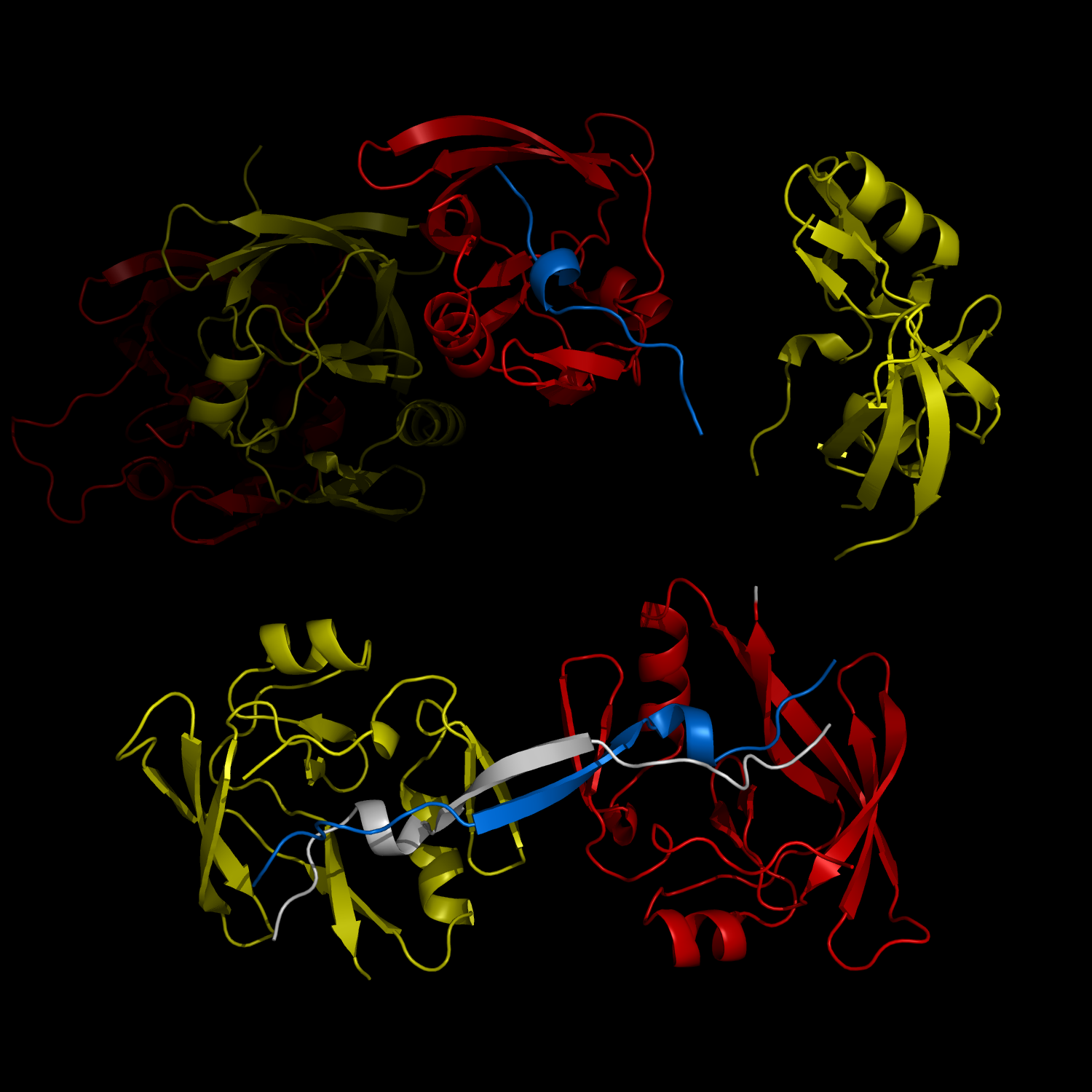 New Structural Insight into Neurodegenerative Disease
A research team from the Korea Advanced Institute of Science and Technology (KAIST) released their results on the structure and molecular details of the neurodegenerative disease-associated protein Ataxin-1. Mutations in Ataxin-1 cause the neurological disease, Spinocerebella Ataxia Type 1 (SCA1), which is characterized by a loss of muscular coordination and balance (ataxia), as is seen in Parkinson’s, Alzheimer’s, and Huntington’s diseases.
SCA1-causing mutations in the ATAXIN1 gene alter the length of a glutamine stretch in the Ataxin-1 protein. The research team provides the first structural insight into the complex formation of ATAXIN-1 with its binding partner, Capicua (CIC). The team, led by Professor Ji-Joon Song from the Department of Biological Sciences at KAIST, solved the structure of Ataxin-1 and CIC complex in atomic level revealing molecular details of the interaction between Ataxin-1 and CIC.
Professor Song explained his recent research work,
“We are able to see the intricate process of complex formation and reconfiguration of the two proteins when they interact with each other. Our work, we expect, will provide a new therapeutic target to modulate SCA1 neurodegenerative disease.”
Understanding structural and molecular details of proteins at the atomic level will help researchers to track the molecular pathogenesis of the disease and, ultimately, design targeted therapies or treatments for patients, rather than just relieving the symptoms of diseases.
Professor Song’s research paper, entitled “Structural Basis of Protein Complex Formation and Reconfiguration by Polyglutamine Disease Protein ATAXIN-1 and Capicua,” will be published in the March 15th issue of Genes & Development (www.genesdev.org).
Complex Formation and Reconfiguration of ATAXIN-1 and Capicua
The complex formation between a polyglutamine disease protein, ATXIN-1 and the transcriptional repressor Capicua (CIC) plays a critical role in SCA 1 pathogenesis. The image shows that the homodimerization of ATXIN-1 (yellow and red) is disrupted upon binding of CIC (blue). Furthermore, the binding of CIC to the ATXIN-1 induces a new form of ATXIN-1 dimerization mediated by CICs (ATXIN-1 AXH domains are shown in yellow and red, and CIC peptides shown in blue and white).
2013.04.02 View 10841
New Structural Insight into Neurodegenerative Disease
A research team from the Korea Advanced Institute of Science and Technology (KAIST) released their results on the structure and molecular details of the neurodegenerative disease-associated protein Ataxin-1. Mutations in Ataxin-1 cause the neurological disease, Spinocerebella Ataxia Type 1 (SCA1), which is characterized by a loss of muscular coordination and balance (ataxia), as is seen in Parkinson’s, Alzheimer’s, and Huntington’s diseases.
SCA1-causing mutations in the ATAXIN1 gene alter the length of a glutamine stretch in the Ataxin-1 protein. The research team provides the first structural insight into the complex formation of ATAXIN-1 with its binding partner, Capicua (CIC). The team, led by Professor Ji-Joon Song from the Department of Biological Sciences at KAIST, solved the structure of Ataxin-1 and CIC complex in atomic level revealing molecular details of the interaction between Ataxin-1 and CIC.
Professor Song explained his recent research work,
“We are able to see the intricate process of complex formation and reconfiguration of the two proteins when they interact with each other. Our work, we expect, will provide a new therapeutic target to modulate SCA1 neurodegenerative disease.”
Understanding structural and molecular details of proteins at the atomic level will help researchers to track the molecular pathogenesis of the disease and, ultimately, design targeted therapies or treatments for patients, rather than just relieving the symptoms of diseases.
Professor Song’s research paper, entitled “Structural Basis of Protein Complex Formation and Reconfiguration by Polyglutamine Disease Protein ATAXIN-1 and Capicua,” will be published in the March 15th issue of Genes & Development (www.genesdev.org).
Complex Formation and Reconfiguration of ATAXIN-1 and Capicua
The complex formation between a polyglutamine disease protein, ATXIN-1 and the transcriptional repressor Capicua (CIC) plays a critical role in SCA 1 pathogenesis. The image shows that the homodimerization of ATXIN-1 (yellow and red) is disrupted upon binding of CIC (blue). Furthermore, the binding of CIC to the ATXIN-1 induces a new form of ATXIN-1 dimerization mediated by CICs (ATXIN-1 AXH domains are shown in yellow and red, and CIC peptides shown in blue and white).
2013.04.02 View 10841 -
Professor Lee Jeong Yong Receives 2012 'KAISTian of the Year' Award
Professor Lee Jeong Yong (Department of Material Science and Engineering) received the 2012 ‘KAISTian of the Year’ Award.
Professor Lee had successfully developed a technique that allowed the observation and analysis of liquid in atomic scale.
The technique is expected to have great impact on nano-material synthesis in solution, explaining electrode and electrolyte reaction, liquid and catalysis reaction research, and etc. and was therefore named as the best experimental accomplishment in KAIST in 2012.
Professor Lee and his team’s finding has been published in the April edition of Science magazine and has had attracted the attention of the world. In addition, BBC News, and Science & Environment reported on the findings as their respective top articles.
The optical microscope is incapable of atomic scale observation and the electron microscopes are capable but because of the vacuum state all liquids undergo evaporation making it impossible to observe liquids in an atomic scale.
Professor Lee’s team wrapped the liquid with a layer of grapheme to prevent evaporation and successfully observed real time the platinum growth process in solution.
Professor Lee’s findings were introduced as an example of exemplar research case in the Presidential address for ‘Science Day’ in April.
2013.01.22 View 11140
-
 Dopant properties of silicon nanowires investigated
Professor Chang Kee Joo
Professor Kee Joo Chang’s research team from the Department of Physics at KAIST has successfully unearthed the properties of boron and phosphorous dopants in silicon nanowires, a material expected to be used in next generation semiconductors. The research team was the first in the world to investigate the movement of boron and phosphorous (impurities or ‘dopants’ added for electrical flow) in oxidized silicon nanowires and study the mechanism behind its deactivation.
It is nearly impossible to develop a silicon based semiconductor thinner than 10nm, even using the most advanced modern technology. However, the thickness of silicon nanowires are within the nano level and hence, allows a higher degree of integration in semiconductors.
For silicon nanowires to carry electricity, small amounts of boron and phosphorous need to be added (‘doping’ process). Compared to silicon, nanowires are harder to create due to the difficulties in the doping process as well as the control of electrical conduction properties.
Professor Chang’s research team improved upon the existing simple model by applying revolutionary quantum simulation theory to create a realistic core-shell atomic model. This research successfully investigated the cause of the escape of boron dopants from the silicon core during oxidation. It was also found that although phosphorous dopants do not escape as oxides, they form electrically deactivated pairs which decreases the efficiency. These phenomena were attributed to the film shape of the nano-wires, which increases the relative surface area compared to a same volume of silicon.
The research results were published in the online September edition of the world renowned Nano Letters.
Figure: The longitudinal section diagram of the Silicon/oxide core-shell model
2012.11.28 View 9592
Dopant properties of silicon nanowires investigated
Professor Chang Kee Joo
Professor Kee Joo Chang’s research team from the Department of Physics at KAIST has successfully unearthed the properties of boron and phosphorous dopants in silicon nanowires, a material expected to be used in next generation semiconductors. The research team was the first in the world to investigate the movement of boron and phosphorous (impurities or ‘dopants’ added for electrical flow) in oxidized silicon nanowires and study the mechanism behind its deactivation.
It is nearly impossible to develop a silicon based semiconductor thinner than 10nm, even using the most advanced modern technology. However, the thickness of silicon nanowires are within the nano level and hence, allows a higher degree of integration in semiconductors.
For silicon nanowires to carry electricity, small amounts of boron and phosphorous need to be added (‘doping’ process). Compared to silicon, nanowires are harder to create due to the difficulties in the doping process as well as the control of electrical conduction properties.
Professor Chang’s research team improved upon the existing simple model by applying revolutionary quantum simulation theory to create a realistic core-shell atomic model. This research successfully investigated the cause of the escape of boron dopants from the silicon core during oxidation. It was also found that although phosphorous dopants do not escape as oxides, they form electrically deactivated pairs which decreases the efficiency. These phenomena were attributed to the film shape of the nano-wires, which increases the relative surface area compared to a same volume of silicon.
The research results were published in the online September edition of the world renowned Nano Letters.
Figure: The longitudinal section diagram of the Silicon/oxide core-shell model
2012.11.28 View 9592 -
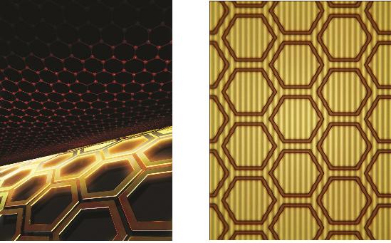 The control of light at the nano-level
Professor Min Bumki
Professor Min Bumki’s research team from the Department of Mechanical Engineering at KAIST have successfully gained control of the transmittance of light in optical devices using graphene* and artificial 2-dimensional metamaterials**.
* Graphene : a thin membrane composed of pure carbon, with atoms arranged in a regular hexagonal pattern
** Metamaterials : artificial materials engineered to have properties that may not be found in nature
The research results were published in the recent online edition (September 30th) of Nature Materials, a sister journal of the world renowned Nature journal, under the title ‘Terahertz waves with gate-controlled active graphene metamaterials’
Since the discovery of graphene in 2004 by Professors Novoselov and Geim from the University of Manchester (2010 Nobel Prize winners in Physics), it has been dubbed “the dream material” because of its outstanding physical properties.
Graphene has been especially praised for its ability to absorb approximately 2.3% of near infrared and visible rays due to its characteristic electron structure. This property allows graphene to be used as a transparent electrode, which is a vital electrical component used in touch screens and solar batteries. However, graphene’s optical transmittance was largely ignored by researchers due to its limited control using electrical methods and its small optical modulation in data transfer.
Professor Min’s team combined 0.34 nanometer-thick graphene with metamaterials to allow a more effective control of light transmittance and greater optical modulation. This graphene metamaterial can be integrated in to a thin and flexible macromolecule substrate which allows the control of transmittance using electric signals.
This research experimentally showed that graphene metamaterials can not only effective control optical transmittance, but can also be used in graphene optical memory devices using electrical hysteresis.
Professor Min said that “this research allows the effective control of light at the nanometer level” and that “this research will help in the development of microscopic optical modulators or memory disks”.
figure 1. The working drawing of graphene metamaterials
figure 2. Conceptual diagram (Left) and microscopic photo (right) of graphene metamaterials
2012.11.23 View 12335
The control of light at the nano-level
Professor Min Bumki
Professor Min Bumki’s research team from the Department of Mechanical Engineering at KAIST have successfully gained control of the transmittance of light in optical devices using graphene* and artificial 2-dimensional metamaterials**.
* Graphene : a thin membrane composed of pure carbon, with atoms arranged in a regular hexagonal pattern
** Metamaterials : artificial materials engineered to have properties that may not be found in nature
The research results were published in the recent online edition (September 30th) of Nature Materials, a sister journal of the world renowned Nature journal, under the title ‘Terahertz waves with gate-controlled active graphene metamaterials’
Since the discovery of graphene in 2004 by Professors Novoselov and Geim from the University of Manchester (2010 Nobel Prize winners in Physics), it has been dubbed “the dream material” because of its outstanding physical properties.
Graphene has been especially praised for its ability to absorb approximately 2.3% of near infrared and visible rays due to its characteristic electron structure. This property allows graphene to be used as a transparent electrode, which is a vital electrical component used in touch screens and solar batteries. However, graphene’s optical transmittance was largely ignored by researchers due to its limited control using electrical methods and its small optical modulation in data transfer.
Professor Min’s team combined 0.34 nanometer-thick graphene with metamaterials to allow a more effective control of light transmittance and greater optical modulation. This graphene metamaterial can be integrated in to a thin and flexible macromolecule substrate which allows the control of transmittance using electric signals.
This research experimentally showed that graphene metamaterials can not only effective control optical transmittance, but can also be used in graphene optical memory devices using electrical hysteresis.
Professor Min said that “this research allows the effective control of light at the nanometer level” and that “this research will help in the development of microscopic optical modulators or memory disks”.
figure 1. The working drawing of graphene metamaterials
figure 2. Conceptual diagram (Left) and microscopic photo (right) of graphene metamaterials
2012.11.23 View 12335