Department+of+Physics
-
 Dr. Se-Jung Kim Receives the Grand Prize at the International Photo and Image Contest on Light
Dr. Se-Jung Kim of the Physics Department at KAIST received the Grand Prize at the 2015 Photo and Image Contest of the International Year of Light and Light-based Technologies.
The United Nations has designated the year 2015 as the International Year of Light and Light-based Technologies.
The Optical Society of Korea celebrated the UN’s designation by hosting an international photo and image contest on the theme of light and optics related technology.
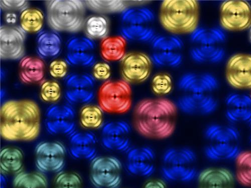
Dr. Kim presented a photo of images taken from a liquid crystal, which was entitled “A Micro Pinwheel.” She took pictures of liquid crystal images with a polarizing microscope and then colored the pictures. The liquid crystal has self-assembled circle domain structures, and each domain can form vortex optics. Her adviser for the project is Professor Yong-Hoon Cho of the Physics Department.
Her work was exhibited during the annual conference of the Optical Society of Korea, which was held on July 13-15, 2015 at Gyeong-Ju Hwabaek International Convention Center. It will also be exhibited at the National Science Museum in Gwacheon and the Kim Dae-Jung Convention Center in Gwangju.
Picture: A Micro Pinwheel
2015.07.31 View 10955
Dr. Se-Jung Kim Receives the Grand Prize at the International Photo and Image Contest on Light
Dr. Se-Jung Kim of the Physics Department at KAIST received the Grand Prize at the 2015 Photo and Image Contest of the International Year of Light and Light-based Technologies.
The United Nations has designated the year 2015 as the International Year of Light and Light-based Technologies.
The Optical Society of Korea celebrated the UN’s designation by hosting an international photo and image contest on the theme of light and optics related technology.
Dr. Kim presented a photo of images taken from a liquid crystal, which was entitled “A Micro Pinwheel.” She took pictures of liquid crystal images with a polarizing microscope and then colored the pictures. The liquid crystal has self-assembled circle domain structures, and each domain can form vortex optics. Her adviser for the project is Professor Yong-Hoon Cho of the Physics Department.
Her work was exhibited during the annual conference of the Optical Society of Korea, which was held on July 13-15, 2015 at Gyeong-Ju Hwabaek International Convention Center. It will also be exhibited at the National Science Museum in Gwacheon and the Kim Dae-Jung Convention Center in Gwangju.
Picture: A Micro Pinwheel
2015.07.31 View 10955 -
 KAIST Undergraduates Organize the Largest Interdisciplinary Conference in Asia
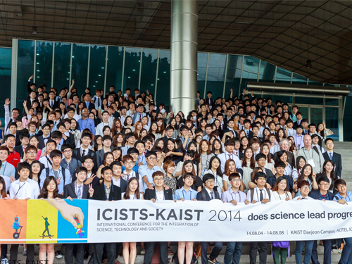
The largest interdisciplinary conference in Asia hosted by KAIST undergraduates for students around the world will be held in KAIST. The organizing committee of International Conference for the Integration of Science, Technology and Society (ICISTS) will hold the ICISTS-KAIST 2015 in KAIST and Hotel ICC from August 3-7, 2015, with around 300 Korean and international participants.
ICISTS-KAIST was established in 2005 to provide an annual platform for students to discuss the integration and the convergence of science, technology and society, regardless of their academic background.
This year’s theme is "Shaping the Future" and the topics for the conference are robotics, medicine, and science communication.
The keynote speakers are Vitalic Buterin, the winner of the World Technology Award in 2014 for the co-creation and invention of Ethereum and Alan Irwin, a well-known scholar of science, technology and society as well as the Dean of Research at the Copenhagen Business School in Denmark.
Other notable speakers include Adam Marcus, a professor of Hematology and Medical Oncology, Emory University School of Medicine; Stefan Lorenz Sorgner, the Director and co-founder of Beyond Humanism Network; Hideto Nakajima, a professor in the Department of History, Philosophy and Social Studies of Science and Technology at Tokyo Institute of Technology; Wendell Wallach, a lecturer at the Yale University Interdisciplinary Center for Bioethics; Jinil Lee, a professor in the Division of Biological Science and Technology at Yonsei University; and Sangwook Kim, an editor of APCTP web journal Crossroads and a professor in the Department of Physics Education, Pusan National University.
Last year, more than 300 students from 50 different countries attended the ICISTS-KAIST 2014 as delegates to exchange their thoughts and ideas on science, technology, and society.
To register for the event, please visit www.icists.org.
2015.07.14 View 8772
KAIST Undergraduates Organize the Largest Interdisciplinary Conference in Asia
The largest interdisciplinary conference in Asia hosted by KAIST undergraduates for students around the world will be held in KAIST. The organizing committee of International Conference for the Integration of Science, Technology and Society (ICISTS) will hold the ICISTS-KAIST 2015 in KAIST and Hotel ICC from August 3-7, 2015, with around 300 Korean and international participants.
ICISTS-KAIST was established in 2005 to provide an annual platform for students to discuss the integration and the convergence of science, technology and society, regardless of their academic background.
This year’s theme is "Shaping the Future" and the topics for the conference are robotics, medicine, and science communication.
The keynote speakers are Vitalic Buterin, the winner of the World Technology Award in 2014 for the co-creation and invention of Ethereum and Alan Irwin, a well-known scholar of science, technology and society as well as the Dean of Research at the Copenhagen Business School in Denmark.
Other notable speakers include Adam Marcus, a professor of Hematology and Medical Oncology, Emory University School of Medicine; Stefan Lorenz Sorgner, the Director and co-founder of Beyond Humanism Network; Hideto Nakajima, a professor in the Department of History, Philosophy and Social Studies of Science and Technology at Tokyo Institute of Technology; Wendell Wallach, a lecturer at the Yale University Interdisciplinary Center for Bioethics; Jinil Lee, a professor in the Division of Biological Science and Technology at Yonsei University; and Sangwook Kim, an editor of APCTP web journal Crossroads and a professor in the Department of Physics Education, Pusan National University.
Last year, more than 300 students from 50 different countries attended the ICISTS-KAIST 2014 as delegates to exchange their thoughts and ideas on science, technology, and society.
To register for the event, please visit www.icists.org.
2015.07.14 View 8772 -
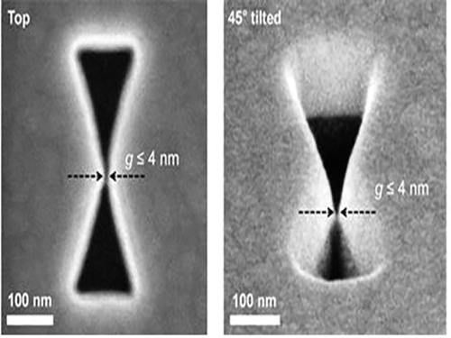 3D Plasmon Antenna Capable of Focusing Light into Few Nanometers
Professors Myung-Ki Kim and Yong-Hee Lee, both of the Physics Department at KAIST, and their research teams have developed a three dimensional (3D) gap-plasmon antenna which can focus light into a space a few nanometers wide. Their research findings were published in the June 10th issue of Nano Letters.
Focusing light into a point-like space is an active research field with many applications. However, concentrating light into a smaller space than its wavelength is often hindered by diffraction. To tackle this problem, many researchers have utilized the plasmonic phenomenon of a metal where light can be confined to a greater extent by overcoming the diffraction limit.
Many researchers have focused on developing a two dimensional (2D) plasmon antenna and were able to focus a light under 5 nanometers wide. However, this 2D antenna revealed a challenge: the light disperses to the opposite end regardless of how small its beam was focused. To solve this difficulty, a 3D structure had to be employed to maximize the light's intensity.
Adopting the proximal focused-ion-beam milling technology, the KAIST research team developed a 3D four nanometer wide gap-plasmon antenna. By squeezing the photons into a 3D nano space of 4 x 10 x 10 nm3 size, the researchers were able to increase the intensity of light by 400,000 times stronger than that of the incident light. Capitalizing on the enhanced intensity of light within the antenna, they intensified the second-harmonic signal and verified that the light was focused in the nano gap by scanning cathodoluminescent images.
The researchers anticipate that this technology will improve the speed of data transfer and processing up to the level of a terahertz (one trillion times per second) and to enlarge the storage volume per unit area on hard disks by 100 times. In addition, high definition images of submolecule size can be taken with actual light, instead of with an electron microscope, while improving the semiconductor process to a smaller size of few nanometers.
Professor Kim said, “A simple yet ingenious idea has shifted the research paradigm from 2D gap-plasmon antennas to 3D antennas. This technology will see numerous applications including in the field of information technology, data storage, imaging medical science, and semiconductor processes.”
The research was sponsored by the National Research Foundation of Korea.
Figure 1: 3D Gap-Plasmon Antenna Structure and Simulation Results
Figure 2 – Constructed 3D Gap-Plasmon Antenna Structure
Figure 3 – Amplified Second Harmonic Signal Generation and Light Focused in the Nano Gap
2015.06.24 View 10685
3D Plasmon Antenna Capable of Focusing Light into Few Nanometers
Professors Myung-Ki Kim and Yong-Hee Lee, both of the Physics Department at KAIST, and their research teams have developed a three dimensional (3D) gap-plasmon antenna which can focus light into a space a few nanometers wide. Their research findings were published in the June 10th issue of Nano Letters.
Focusing light into a point-like space is an active research field with many applications. However, concentrating light into a smaller space than its wavelength is often hindered by diffraction. To tackle this problem, many researchers have utilized the plasmonic phenomenon of a metal where light can be confined to a greater extent by overcoming the diffraction limit.
Many researchers have focused on developing a two dimensional (2D) plasmon antenna and were able to focus a light under 5 nanometers wide. However, this 2D antenna revealed a challenge: the light disperses to the opposite end regardless of how small its beam was focused. To solve this difficulty, a 3D structure had to be employed to maximize the light's intensity.
Adopting the proximal focused-ion-beam milling technology, the KAIST research team developed a 3D four nanometer wide gap-plasmon antenna. By squeezing the photons into a 3D nano space of 4 x 10 x 10 nm3 size, the researchers were able to increase the intensity of light by 400,000 times stronger than that of the incident light. Capitalizing on the enhanced intensity of light within the antenna, they intensified the second-harmonic signal and verified that the light was focused in the nano gap by scanning cathodoluminescent images.
The researchers anticipate that this technology will improve the speed of data transfer and processing up to the level of a terahertz (one trillion times per second) and to enlarge the storage volume per unit area on hard disks by 100 times. In addition, high definition images of submolecule size can be taken with actual light, instead of with an electron microscope, while improving the semiconductor process to a smaller size of few nanometers.
Professor Kim said, “A simple yet ingenious idea has shifted the research paradigm from 2D gap-plasmon antennas to 3D antennas. This technology will see numerous applications including in the field of information technology, data storage, imaging medical science, and semiconductor processes.”
The research was sponsored by the National Research Foundation of Korea.
Figure 1: 3D Gap-Plasmon Antenna Structure and Simulation Results
Figure 2 – Constructed 3D Gap-Plasmon Antenna Structure
Figure 3 – Amplified Second Harmonic Signal Generation and Light Focused in the Nano Gap
2015.06.24 View 10685 -
 Fast, Accurate 3D Imaging to Track Optically-Trapped Particles
KAIST researchers published an article on the development of a novel technique to precisely track the 3-D positions of optically-trapped particles having complicated geometry in high speed in the April 2015 issue of Optica.
Optical tweezers have been used as an invaluable tool for exerting micro-scale force on microscopic particles and manipulating three-dimensional (3-D) positions of particles. Optical tweezers employ a tightly-focused laser whose beam diameter is smaller than one micrometer (1/100 of hair thickness), which generates attractive force on neighboring microscopic particles moving toward the beam focus. Controlling the positions of the beam focus enabled researchers to hold the particles and move them freely to other locations so they coined the name “optical tweezers.”
To locate the optically-trapped particles by a laser beam, optical microscopes have usually been employed. Optical microscopes measure light signals scattered by the optically-trapped microscopic particles and the positions of the particles in two dimensions. However, it was difficult to quantify the particles’ precise positions along the optic axis, the direction of the beam, from a single image, which is analogous to the difficulty of determining the front and rear positions of objects when closing an eye due to a lack of depth perception. Furthermore, it became more difficult to measure precisely 3-D positions of particles when scattered light signals were distorted by optically-trapped particles having complicated shapes or other particles occlude the target object along the optic axis.
Professor YongKeun Park and his research team in the Department of Physics at the Korea Advanced Institute of Science and Technology (KAIST) employed an optical diffraction tomography (ODT) technique to measure 3-D positions of optically-trapped particles in high speed. The principle of ODT is similar to X-ray CT imaging commonly used in hospitals for visualizing the internal organs of patients. Like X-ray CT imaging, which takes several images from various illumination angles, ODT measures 3-D images of optically-trapped particles by illuminating them with a laser beam in various incidence angles.
The KAIST team used optical tweezers to trap a glass bead with a diameter of 2 micrometers, and moved the bead toward a white blood cell having complicated internal structures. The team measured the 3-D dynamics of the white blood cell as it responded to an approaching glass bead via ODT in the high acquisition rate of 60 images per second. Since the white blood cell screens the glass bead along an optic axis, a conventionally-used optical microscope could not determine the 3-D positions of the glass bead. In contrast, the present method employing ODT localized the 3-D positions of the bead precisely as well as measured the composition of the internal materials of the bead and the white blood cell simultaneously.
Professor Park said, “Our technique has the advantage of measuring the 3-D positions and internal structures of optically-trapped particles in high speed without labelling exogenous fluorescent agents and can be applied in various fields including physics, optics, nanotechnology, and medical science.”
Kyoohyun Kim, the lead author of this paper (“Simultaneous 3D Visualization and Position Tracking of Optically Trapped Particles Using Optical Diffraction Tomography”), added, “This ODT technique can also apply to cellular-level surgeries where optical tweezers are used to manipulate intracellular organelles and to display in real time and in 3-D the images of the reaction of the cell membrane and nucleus during the operation or monitoring the recovery process of the cells from the surgery.”
The research results were published as the cover article in the April 2014 issue of Optica, the newest journal launched last year by the Optical Society of America (OSA) for rapid dissemination of high-impact results related to optics.
Figure 1: This picture shows the concept image of tweezing an optically-trapped glass bead on the cellular membrane of a white blood cell.
Figure 2: High-speed 3-D images produced from optical diffraction tomography technique
2015.04.24 View 12328
Fast, Accurate 3D Imaging to Track Optically-Trapped Particles
KAIST researchers published an article on the development of a novel technique to precisely track the 3-D positions of optically-trapped particles having complicated geometry in high speed in the April 2015 issue of Optica.
Optical tweezers have been used as an invaluable tool for exerting micro-scale force on microscopic particles and manipulating three-dimensional (3-D) positions of particles. Optical tweezers employ a tightly-focused laser whose beam diameter is smaller than one micrometer (1/100 of hair thickness), which generates attractive force on neighboring microscopic particles moving toward the beam focus. Controlling the positions of the beam focus enabled researchers to hold the particles and move them freely to other locations so they coined the name “optical tweezers.”
To locate the optically-trapped particles by a laser beam, optical microscopes have usually been employed. Optical microscopes measure light signals scattered by the optically-trapped microscopic particles and the positions of the particles in two dimensions. However, it was difficult to quantify the particles’ precise positions along the optic axis, the direction of the beam, from a single image, which is analogous to the difficulty of determining the front and rear positions of objects when closing an eye due to a lack of depth perception. Furthermore, it became more difficult to measure precisely 3-D positions of particles when scattered light signals were distorted by optically-trapped particles having complicated shapes or other particles occlude the target object along the optic axis.
Professor YongKeun Park and his research team in the Department of Physics at the Korea Advanced Institute of Science and Technology (KAIST) employed an optical diffraction tomography (ODT) technique to measure 3-D positions of optically-trapped particles in high speed. The principle of ODT is similar to X-ray CT imaging commonly used in hospitals for visualizing the internal organs of patients. Like X-ray CT imaging, which takes several images from various illumination angles, ODT measures 3-D images of optically-trapped particles by illuminating them with a laser beam in various incidence angles.
The KAIST team used optical tweezers to trap a glass bead with a diameter of 2 micrometers, and moved the bead toward a white blood cell having complicated internal structures. The team measured the 3-D dynamics of the white blood cell as it responded to an approaching glass bead via ODT in the high acquisition rate of 60 images per second. Since the white blood cell screens the glass bead along an optic axis, a conventionally-used optical microscope could not determine the 3-D positions of the glass bead. In contrast, the present method employing ODT localized the 3-D positions of the bead precisely as well as measured the composition of the internal materials of the bead and the white blood cell simultaneously.
Professor Park said, “Our technique has the advantage of measuring the 3-D positions and internal structures of optically-trapped particles in high speed without labelling exogenous fluorescent agents and can be applied in various fields including physics, optics, nanotechnology, and medical science.”
Kyoohyun Kim, the lead author of this paper (“Simultaneous 3D Visualization and Position Tracking of Optically Trapped Particles Using Optical Diffraction Tomography”), added, “This ODT technique can also apply to cellular-level surgeries where optical tweezers are used to manipulate intracellular organelles and to display in real time and in 3-D the images of the reaction of the cell membrane and nucleus during the operation or monitoring the recovery process of the cells from the surgery.”
The research results were published as the cover article in the April 2014 issue of Optica, the newest journal launched last year by the Optical Society of America (OSA) for rapid dissemination of high-impact results related to optics.
Figure 1: This picture shows the concept image of tweezing an optically-trapped glass bead on the cellular membrane of a white blood cell.
Figure 2: High-speed 3-D images produced from optical diffraction tomography technique
2015.04.24 View 12328 -
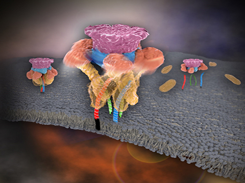 Mystery in Membrane Traffic How NSF Disassembles Single SNAR Complex Solved
KAIST researchers discovered that the protein N-ethylmaleimide-sensitive factor (NSF) unravels a single SNARE complex using one round ATP turnover by tearing the complex with a single burst, contradicting a previous theory that it unwinds in a processive manner.
In 2013, James E. Rothman, Randy W. Schekman, and Thomas C. Südhof won the Nobel Prize in Physiology or Medicine for their discoveries of molecular machineries for vesicle trafficking, a major transport system in cells for maintaining cellular processes. Vesicle traffic acts as a kind of “home-delivery service” in cells. Vesicles package and deliver materials such as proteins and hormones from one cell organelle to another. Then it releases its contents by fusing with the target organelle’s membrane. One example of vesicle traffic is in neuronal communications, where neurotransmitters are released from a neuron. Some of the key proteins for vesicle traffic discovered by the Nobel Prize winners were N-ethylmaleimide-sensitive factor (NSF), alpha-soluble NSF attachment protein (α-SNAP), and soluble SNAP receptors (SNAREs).
SNARE proteins are known as the minimal machinery for membrane fusion. To induce membrane fusion, the proteins combine to form a SNARE complex in a four helical bundle, and NSF and α-SNAP disassemble the SNARE complex for reuse. In particular, NSF can bind an energy source molecule, adenosine triphosphate (ATP), and the ATP-bound NSF develops internal tension via cleavage of ATP. This process is used to exert great force on SNARE complexes, eventually pulling them apart. However, although about 30 years have passed since the Nobel Prize winners’ discovery, how NSF/α-SNAP disassembled the SNARE complex remained a mystery to scientists due to a lack in methodology.
In a recent issue of Science, published on March 27, 2015, a research team, led by Tae-Young Yoon of the Department of Physics at the Korea Advanced Institute of Science and Technology (KAIST) and Reinhard Jahn of the Department of Neurobiology of the Max-Planck-Institute for Biophysical Chemistry, reports that NSF/α-SNAP disassemble a single SNARE complex using various single-molecule biophysical methods that allow them to monitor and manipulate individual protein complexes.
“We have learned that NSF releases energy in a burst within 20 milliseconds to “tear” the SNARE complex apart in a one-step global unfolding reaction, which is immediately followed by the release of SNARE proteins,” said Yoon.
Previously, it was believed that NSF disassembled a SNARE complex by unwinding it in a processive manner. Also, largely unexplained was how many cycles of ATP hydrolysis were required and how these cycles were connected to the disassembly of the SNARE complex.
Yoon added, “From our research, we found that NSF requires hydrolysis of ATPs that were already bound before it attached to the SNAREs—which means that only one round of an ATP turnover is sufficient for SNARE complex disassembly. Moreover, this is possible because NSF pulls a SNARE complex apart by building up the energy from individual ATPs and releasing it at once, yielding a “spring-loaded” mechanism.”
NSF is a member of the ATPases associated with various cellular activities family (AAA+ ATPase), which is essential for many cellular functions such as DNA replication and protein degradation, membrane fusion, microtubule severing, peroxisome biogenesis, signal transduction, and the regulation of gene expression. This research has added valuable new insights and hints for studying AAA+ ATPase proteins, which are crucial for various living beings.
The title of the research paper is “Spring-loaded unraveling of a single SNARE complex by NSF in one round of ATP turnover.” (DOI: 10.1126/science.aaa5267)
Youtube Link: https://www.youtube.com/watch?v=FqTSYHtyHWE&feature=youtu.be
Picture 1. Working model of how NSF/α-SNAP disassemble a single SNARE complex
Picture 2. After neurotransmitter release, NSF disassembles a single SNARE complex using a single round of ATP turnover in a single burst reaction.
2015.03.28 View 11267
Mystery in Membrane Traffic How NSF Disassembles Single SNAR Complex Solved
KAIST researchers discovered that the protein N-ethylmaleimide-sensitive factor (NSF) unravels a single SNARE complex using one round ATP turnover by tearing the complex with a single burst, contradicting a previous theory that it unwinds in a processive manner.
In 2013, James E. Rothman, Randy W. Schekman, and Thomas C. Südhof won the Nobel Prize in Physiology or Medicine for their discoveries of molecular machineries for vesicle trafficking, a major transport system in cells for maintaining cellular processes. Vesicle traffic acts as a kind of “home-delivery service” in cells. Vesicles package and deliver materials such as proteins and hormones from one cell organelle to another. Then it releases its contents by fusing with the target organelle’s membrane. One example of vesicle traffic is in neuronal communications, where neurotransmitters are released from a neuron. Some of the key proteins for vesicle traffic discovered by the Nobel Prize winners were N-ethylmaleimide-sensitive factor (NSF), alpha-soluble NSF attachment protein (α-SNAP), and soluble SNAP receptors (SNAREs).
SNARE proteins are known as the minimal machinery for membrane fusion. To induce membrane fusion, the proteins combine to form a SNARE complex in a four helical bundle, and NSF and α-SNAP disassemble the SNARE complex for reuse. In particular, NSF can bind an energy source molecule, adenosine triphosphate (ATP), and the ATP-bound NSF develops internal tension via cleavage of ATP. This process is used to exert great force on SNARE complexes, eventually pulling them apart. However, although about 30 years have passed since the Nobel Prize winners’ discovery, how NSF/α-SNAP disassembled the SNARE complex remained a mystery to scientists due to a lack in methodology.
In a recent issue of Science, published on March 27, 2015, a research team, led by Tae-Young Yoon of the Department of Physics at the Korea Advanced Institute of Science and Technology (KAIST) and Reinhard Jahn of the Department of Neurobiology of the Max-Planck-Institute for Biophysical Chemistry, reports that NSF/α-SNAP disassemble a single SNARE complex using various single-molecule biophysical methods that allow them to monitor and manipulate individual protein complexes.
“We have learned that NSF releases energy in a burst within 20 milliseconds to “tear” the SNARE complex apart in a one-step global unfolding reaction, which is immediately followed by the release of SNARE proteins,” said Yoon.
Previously, it was believed that NSF disassembled a SNARE complex by unwinding it in a processive manner. Also, largely unexplained was how many cycles of ATP hydrolysis were required and how these cycles were connected to the disassembly of the SNARE complex.
Yoon added, “From our research, we found that NSF requires hydrolysis of ATPs that were already bound before it attached to the SNAREs—which means that only one round of an ATP turnover is sufficient for SNARE complex disassembly. Moreover, this is possible because NSF pulls a SNARE complex apart by building up the energy from individual ATPs and releasing it at once, yielding a “spring-loaded” mechanism.”
NSF is a member of the ATPases associated with various cellular activities family (AAA+ ATPase), which is essential for many cellular functions such as DNA replication and protein degradation, membrane fusion, microtubule severing, peroxisome biogenesis, signal transduction, and the regulation of gene expression. This research has added valuable new insights and hints for studying AAA+ ATPase proteins, which are crucial for various living beings.
The title of the research paper is “Spring-loaded unraveling of a single SNARE complex by NSF in one round of ATP turnover.” (DOI: 10.1126/science.aaa5267)
Youtube Link: https://www.youtube.com/watch?v=FqTSYHtyHWE&feature=youtu.be
Picture 1. Working model of how NSF/α-SNAP disassemble a single SNARE complex
Picture 2. After neurotransmitter release, NSF disassembles a single SNARE complex using a single round of ATP turnover in a single burst reaction.
2015.03.28 View 11267 -
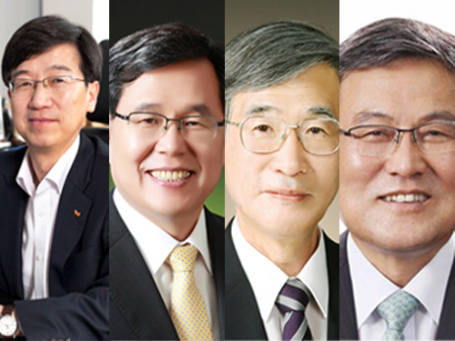 KAIST Announces the Recipients of Distinguished Alumni Awards
The KAIST Alumni Association (KAA) announced four “Proud KAIST Alumni” awards recipients for the year 2014: Sung-Wook Park, the Chief Executive Officer and President of SK Hynix; Seung Ho Shin, the President of Kangwon National University; Kew-Ho Lee, the President of the Korea Research Institute of Chemical Technology; and Mun-Kee Choi, the former Minister of Science, ICT and Future Planning of the Republic of Korea. The award ceremony took place during the 2015 KAA’s New Year's ceremony on January 17, 2015 at the Palace Hotel in Seoul.
Sung-Wook Park (M.S. ’82 and Ph.D. ’88, Department of Materials Science and Engineering), the Chief Executive Officer and President of SK Hynix, has worked as an expert in the field of memory semi-conductors for the past 30 years. He developed innovative technology and improved production efficiency, enabling the Korean semi-conductor industry to become a global leader.
Seung Ho Shin (M.S. ’79 and Ph.D. ’87, Department of Physics), the President of Kangwon National University (KNU), worked in the field of optical information processing, producing excellent research achievements and teaching the next generation of scientists. As the president of KNU, he has set an exemplary leadership in higher education.
Kew-Ho Lee (M.S. ’75, Department of Chemistry), the President of the Korea Research Institute of Chemical Technology, pioneered the field of separation film production which contributed greatly to Korean technological developments. He led several domestic and international societies to facilitate dynamic exchanges between industry and academia and with the international community.
Mun-Kee Choi (M.S. ’76, Department of Industrial and Systems Engineering), the former Minister of Science, ICT and Future Planning, the Republic of Korea, is a great contributor to the information and communications technology in Korea, working as a leader in the field of broadband integrated service digital network. He is also an educator for gifted students in science and technology, and a manager of the Electronics and Telecommunications Research Institute.
The Alumni Association established the “Proud KAIST Alumni Awards” in 1992 to recognize its alumni’s outstanding contributions to Korea and KAIST.
Pictured from left to right, Sung-Wook Park (the Chief Executive Officer and President of SK Hynix), Seung Ho Shin (the President of Kangwon National University), Kew-Ho Lee (the President of the Korea Research Institute of Chemical Technology), and Mun-Kee Choi (the former Minister of Science, ICT and Future Planning)
2015.01.19 View 15666
KAIST Announces the Recipients of Distinguished Alumni Awards
The KAIST Alumni Association (KAA) announced four “Proud KAIST Alumni” awards recipients for the year 2014: Sung-Wook Park, the Chief Executive Officer and President of SK Hynix; Seung Ho Shin, the President of Kangwon National University; Kew-Ho Lee, the President of the Korea Research Institute of Chemical Technology; and Mun-Kee Choi, the former Minister of Science, ICT and Future Planning of the Republic of Korea. The award ceremony took place during the 2015 KAA’s New Year's ceremony on January 17, 2015 at the Palace Hotel in Seoul.
Sung-Wook Park (M.S. ’82 and Ph.D. ’88, Department of Materials Science and Engineering), the Chief Executive Officer and President of SK Hynix, has worked as an expert in the field of memory semi-conductors for the past 30 years. He developed innovative technology and improved production efficiency, enabling the Korean semi-conductor industry to become a global leader.
Seung Ho Shin (M.S. ’79 and Ph.D. ’87, Department of Physics), the President of Kangwon National University (KNU), worked in the field of optical information processing, producing excellent research achievements and teaching the next generation of scientists. As the president of KNU, he has set an exemplary leadership in higher education.
Kew-Ho Lee (M.S. ’75, Department of Chemistry), the President of the Korea Research Institute of Chemical Technology, pioneered the field of separation film production which contributed greatly to Korean technological developments. He led several domestic and international societies to facilitate dynamic exchanges between industry and academia and with the international community.
Mun-Kee Choi (M.S. ’76, Department of Industrial and Systems Engineering), the former Minister of Science, ICT and Future Planning, the Republic of Korea, is a great contributor to the information and communications technology in Korea, working as a leader in the field of broadband integrated service digital network. He is also an educator for gifted students in science and technology, and a manager of the Electronics and Telecommunications Research Institute.
The Alumni Association established the “Proud KAIST Alumni Awards” in 1992 to recognize its alumni’s outstanding contributions to Korea and KAIST.
Pictured from left to right, Sung-Wook Park (the Chief Executive Officer and President of SK Hynix), Seung Ho Shin (the President of Kangwon National University), Kew-Ho Lee (the President of the Korea Research Institute of Chemical Technology), and Mun-Kee Choi (the former Minister of Science, ICT and Future Planning)
2015.01.19 View 15666 -
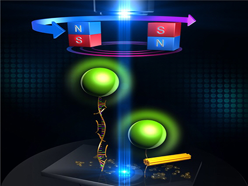 An Advanced Method of DNA Nanostructure Formation Developed
Professor Tae-Young Yoon’s research team from the Department of Physics at KAIST has developed a new method to form DNA nanostructures by using magnetic tweezers to observe and to induce the formation of the structure in real time.
Unlike traditional designs of "DNA origami" which relies on thermal or chemical annealing methods, the new technology utilizes a completely different dynamic in DNA folding. This allows the folding to be done within only ten minutes.
Developed in 2006, the "DNA origami" allows a long skeleton of DNA to be folded into an arbitrary structure by using small stapler DNA pieces. This has been a prominent method in DNA nanotechnology.
However, the traditional technology which adopts thermal processes could not control the DNA formation during the folding because every interaction among DNAs occurs simultaneously. Thus, the thermal processes, which take dozens of hours to complete, had to be repeated multiple times in order to find the optimal condition.
The research team designed a DNA folding using uni-molecular magnetic tweezers that applied force to a single DNA molecule while measuring the state of the DNA. Through this technology, they were able to induce the formation of DNA nanostructure and observe it at the same time.
During high temperature heat treatment, the first stage of conventional thermal processes, the internal structure of the long skeleton DNA untangles. To induce such state, after attaching one side of the skeleton DNA to the surface of glass and the other side to a magnetic material, the team unfolded the internal structure of the DNA by pulling the two sides apart with magnetic force.
Unlike the conventional thermal processes, this method lets the stapler DNA swiftly adhere to the skeleton DNA within a minute because the sites are revealed at room temperature.
After the stapler pieces connected to the skeleton, the team removed the magnetic force. Next, the structure folded through self-assembly as the stapler DNAs stuck to different sites on the skeleton DNA.
Professor Yoon said, “With the existing thermal methods, we could not differentiate the reactions of the DNA because the response of each DNA pieces mutually interacted with each other.” He added that “Using the magnetic tweezers, we were able to sort the process of DNA nanostructure formation into a series of reactions of DNA molecules that are well known, and shorten the time taken for formation in only ten minutes.”
He commented, “This nanostructure formation method will enable us to create more intricate and desirable DNA nanostructures by programming the folding of DNA origami structures.”
Conducted by Dr. Woori Bae under the guidance of Professor Yoon, the research findings were published online in the December 4th issue of Nature Communications.
Figure 1: Uni-molecular magnetic tweezers orchestrating the DNA nanostructure formation
Figure 2: The evolution of DNA nanostructure formation using magnetic tweezers. The DNA nanostructure with a 21-nanometer size was formed in about eight minutes.
2015.01.06 View 7738
An Advanced Method of DNA Nanostructure Formation Developed
Professor Tae-Young Yoon’s research team from the Department of Physics at KAIST has developed a new method to form DNA nanostructures by using magnetic tweezers to observe and to induce the formation of the structure in real time.
Unlike traditional designs of "DNA origami" which relies on thermal or chemical annealing methods, the new technology utilizes a completely different dynamic in DNA folding. This allows the folding to be done within only ten minutes.
Developed in 2006, the "DNA origami" allows a long skeleton of DNA to be folded into an arbitrary structure by using small stapler DNA pieces. This has been a prominent method in DNA nanotechnology.
However, the traditional technology which adopts thermal processes could not control the DNA formation during the folding because every interaction among DNAs occurs simultaneously. Thus, the thermal processes, which take dozens of hours to complete, had to be repeated multiple times in order to find the optimal condition.
The research team designed a DNA folding using uni-molecular magnetic tweezers that applied force to a single DNA molecule while measuring the state of the DNA. Through this technology, they were able to induce the formation of DNA nanostructure and observe it at the same time.
During high temperature heat treatment, the first stage of conventional thermal processes, the internal structure of the long skeleton DNA untangles. To induce such state, after attaching one side of the skeleton DNA to the surface of glass and the other side to a magnetic material, the team unfolded the internal structure of the DNA by pulling the two sides apart with magnetic force.
Unlike the conventional thermal processes, this method lets the stapler DNA swiftly adhere to the skeleton DNA within a minute because the sites are revealed at room temperature.
After the stapler pieces connected to the skeleton, the team removed the magnetic force. Next, the structure folded through self-assembly as the stapler DNAs stuck to different sites on the skeleton DNA.
Professor Yoon said, “With the existing thermal methods, we could not differentiate the reactions of the DNA because the response of each DNA pieces mutually interacted with each other.” He added that “Using the magnetic tweezers, we were able to sort the process of DNA nanostructure formation into a series of reactions of DNA molecules that are well known, and shorten the time taken for formation in only ten minutes.”
He commented, “This nanostructure formation method will enable us to create more intricate and desirable DNA nanostructures by programming the folding of DNA origami structures.”
Conducted by Dr. Woori Bae under the guidance of Professor Yoon, the research findings were published online in the December 4th issue of Nature Communications.
Figure 1: Uni-molecular magnetic tweezers orchestrating the DNA nanostructure formation
Figure 2: The evolution of DNA nanostructure formation using magnetic tweezers. The DNA nanostructure with a 21-nanometer size was formed in about eight minutes.
2015.01.06 View 7738 -
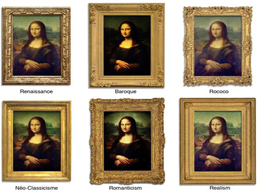 How Science Understands the Beauty of Fine Arts from the Medieval Era to the 19th Century
A research team, consisting of Professor Hawoong Jeong of the Department of Physics at KAIST and Assistant Professor Seung-Woo Son of the Department of Applied Physics at Hanyang University, conducted a research project to understand visual representations through the eyes of science, i.e., quantitative analyses. Researchers took a sample of reproductions of European paintings from the 11th to the early 19th centuries and analyzed them based on three elements: the usage of color, the variety of painted colors, and the brightness of the images.
For the large-scale quantitative analysis, the research team utilized digital images of the paintings obtained from the Web Gallery of Art, a virtual museum and searchable database of European fine arts that includes over 29,000 pieces, ranging from the years 1000 to 1850. The Web Gallery classifies paintings into ten art historical periods such as Medieval, Renaissance, Mannerist, Baroque, Rococo, Romantic, and Realist.
For each period, researchers investigated the frequency of certain colors which appear in paintings and examined the variety of painted colors, paying particular attention to paintings created by two iconoclastic artists from different eras: Pieter Bruegel the Elder and Jackson Pollock. In their works, the researchers discovered that specific pigments were preferred in each period, the result of reflecting historical facts into fine arts. For example, certain rare colors were used in the medieval age for political and religious reasons, and artists in that era employed a technique to layer one color over another dry color in order to express mixed colors, resulting in thickly textured brushstrokes because they considered mixing colors impure. Moreover, oil colors and color mixing techniques were not fully developed until the Renaissance age.
According to the research team, fewer numbers of colors were used before the 20th century, and the introduction of new expressionist tools, like the use of pastels and fingers directly on canvas, and painting techniques, such as “chiaroscuro” and “sfumato,” made much more colorful and natural expressions possible after the Renaissance period. The team said that the color arrangement of Jackson Pollock’s drip paintings differed substantially from other paintings, showing randomness, especially in the spatial arrangement of colors.
Researchers also examined one of the artistic effects applied to paintings, contrast, an important element to express shape and space in two dimensional fine arts. Among various types of contrasts, they said, brightness contrast is the most important in art history due to the cultural background of Europe which usually adopts the contrast of light and darkness as a metaphorical expression. Taking the color information of pixels and their spatial arrangement, the researchers studied the prevalence of brightness contrast in European paintings over ten artistic periods by developing a correlation function to measure the contrast. These mathematical measurements quantitatively describe the birth of new painting techniques including chiaroscuro and sfumato and their increasing use. For instance, in the medieval age, the contour of objects or images in paintings was vague, but it became much clearer later in the Romantic period.
Professor Jeong said, “The complexity of the material world has been a long-lasting topic of interest in natural science, but research in the structural complexity of art and humanities has only begun since the development of the Internet, with the availability of big data in these fields. Our research is a meaningful attempt to understand the underling intricacy of art and humanities based on a scientific approach, expressed quantitatively.”
The research results were published online on December 11, 2014 in Scientific Reports, entitled “Large-Scale Quantitative Analysis of Painting Arts.” The paper was also selected as one of the weekly research highlights by Nature and is noted on its online journal’s website.
YouTube link on “the brightness contrast”: http://youtu.be/SFo0h1EU2aw
Figure 1: Constructing brightness surfaces and measuring roughness exponents
Figure 2: Visual representations of Mona Lisa painted by Leonardo da Vinci, which was reproduced in accordance with the art historical periods
Figure 3: The screenshot of Nature online webpage
2014.12.23 View 8994
How Science Understands the Beauty of Fine Arts from the Medieval Era to the 19th Century
A research team, consisting of Professor Hawoong Jeong of the Department of Physics at KAIST and Assistant Professor Seung-Woo Son of the Department of Applied Physics at Hanyang University, conducted a research project to understand visual representations through the eyes of science, i.e., quantitative analyses. Researchers took a sample of reproductions of European paintings from the 11th to the early 19th centuries and analyzed them based on three elements: the usage of color, the variety of painted colors, and the brightness of the images.
For the large-scale quantitative analysis, the research team utilized digital images of the paintings obtained from the Web Gallery of Art, a virtual museum and searchable database of European fine arts that includes over 29,000 pieces, ranging from the years 1000 to 1850. The Web Gallery classifies paintings into ten art historical periods such as Medieval, Renaissance, Mannerist, Baroque, Rococo, Romantic, and Realist.
For each period, researchers investigated the frequency of certain colors which appear in paintings and examined the variety of painted colors, paying particular attention to paintings created by two iconoclastic artists from different eras: Pieter Bruegel the Elder and Jackson Pollock. In their works, the researchers discovered that specific pigments were preferred in each period, the result of reflecting historical facts into fine arts. For example, certain rare colors were used in the medieval age for political and religious reasons, and artists in that era employed a technique to layer one color over another dry color in order to express mixed colors, resulting in thickly textured brushstrokes because they considered mixing colors impure. Moreover, oil colors and color mixing techniques were not fully developed until the Renaissance age.
According to the research team, fewer numbers of colors were used before the 20th century, and the introduction of new expressionist tools, like the use of pastels and fingers directly on canvas, and painting techniques, such as “chiaroscuro” and “sfumato,” made much more colorful and natural expressions possible after the Renaissance period. The team said that the color arrangement of Jackson Pollock’s drip paintings differed substantially from other paintings, showing randomness, especially in the spatial arrangement of colors.
Researchers also examined one of the artistic effects applied to paintings, contrast, an important element to express shape and space in two dimensional fine arts. Among various types of contrasts, they said, brightness contrast is the most important in art history due to the cultural background of Europe which usually adopts the contrast of light and darkness as a metaphorical expression. Taking the color information of pixels and their spatial arrangement, the researchers studied the prevalence of brightness contrast in European paintings over ten artistic periods by developing a correlation function to measure the contrast. These mathematical measurements quantitatively describe the birth of new painting techniques including chiaroscuro and sfumato and their increasing use. For instance, in the medieval age, the contour of objects or images in paintings was vague, but it became much clearer later in the Romantic period.
Professor Jeong said, “The complexity of the material world has been a long-lasting topic of interest in natural science, but research in the structural complexity of art and humanities has only begun since the development of the Internet, with the availability of big data in these fields. Our research is a meaningful attempt to understand the underling intricacy of art and humanities based on a scientific approach, expressed quantitatively.”
The research results were published online on December 11, 2014 in Scientific Reports, entitled “Large-Scale Quantitative Analysis of Painting Arts.” The paper was also selected as one of the weekly research highlights by Nature and is noted on its online journal’s website.
YouTube link on “the brightness contrast”: http://youtu.be/SFo0h1EU2aw
Figure 1: Constructing brightness surfaces and measuring roughness exponents
Figure 2: Visual representations of Mona Lisa painted by Leonardo da Vinci, which was reproduced in accordance with the art historical periods
Figure 3: The screenshot of Nature online webpage
2014.12.23 View 8994 -
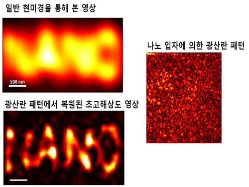 Ultra-high Resolution 2-dimentional Real-time Image Capture with Super Lens
Applications to high-precision semiconductor processing or intracellular structures observation are possible.
A joint research team led by Professors Yongkeun Park and Yong-Hoon Cho from the Department of Physics, KAIST, has succeeded in capturing real-time 2D images at a resolution of 100 nm (nanometers), which was impossible with optical lens due to the diffraction limit of light until now. Its future application includes high-precision semiconductor manufacturing process or observation of intracellular structures.
This research follows the past research of the super-lens developed by Professor Park last April, using paint spray to observe images that have three times higher resolution than those discovered by conventional optical lens.
Since optical lens utilize the refraction of light, the diffraction limit, which prevents achieving focus smaller than the wavelength of light, has always been a barrier for acquiring high-resolution images. In the past, it was impossible to observe objects less than the size of 200 to 300 nm in the visible light spectrum.
In order to solve the problem of near-field extinction due to scattering of light, the research team used spray paint consisting of nano-particles massed with dense scattering materials to obtain high-resolution information.
Then, by calculating and restoring the first scattering shape of light using the time reversibility of light, the researchers were able to overcome the diffraction limit. The original position of an object to be observed is obtained by deriving the complex trajectory of the light, and reversing the time to locate the particular position of the object.
Professor Park said, “This new technology can be used as the core technology in all fields which require optical measurement and control. The existing electron microscopy cannot observe cells without destroying them, but the new technology allows us to visualize at ultra-high resolution without destruction.”
The research results were published online in the 9th edition of Physical Review Letters, a prestigious international journal in the field of physics.
2014.09.23 View 10627
Ultra-high Resolution 2-dimentional Real-time Image Capture with Super Lens
Ultra-high Resolution 2-dimentional Real-time Image Capture with Super Lens
Applications to high-precision semiconductor processing or intracellular structures observation are possible.
A joint research team led by Professors Yongkeun Park and Yong-Hoon Cho from the Department of Physics, KAIST, has succeeded in capturing real-time 2D images at a resolution of 100 nm (nanometers), which was impossible with optical lens due to the diffraction limit of light until now. Its future application includes high-precision semiconductor manufacturing process or observation of intracellular structures.
This research follows the past research of the super-lens developed by Professor Park last April, using paint spray to observe images that have three times higher resolution than those discovered by conventional optical lens.
Since optical lens utilize the refraction of light, the diffraction limit, which prevents achieving focus smaller than the wavelength of light, has always been a barrier for acquiring high-resolution images. In the past, it was impossible to observe objects less than the size of 200 to 300 nm in the visible light spectrum.
In order to solve the problem of near-field extinction due to scattering of light, the research team used spray paint consisting of nano-particles massed with dense scattering materials to obtain high-resolution information.
Then, by calculating and restoring the first scattering shape of light using the time reversibility of light, the researchers were able to overcome the diffraction limit. The original position of an object to be observed is obtained by deriving the complex trajectory of the light, and reversing the time to locate the particular position of the object.
Professor Park said, “This new technology can be used as the core technology in all fields which require optical measurement and control. The existing electron microscopy cannot observe cells without destroying them, but the new technology allows us to visualize at ultra-high resolution without destruction.”
The research results were published online in the 9th edition of Physical Review Letters, a prestigious international journal in the field of physics.
2014.09.23 View 10627 -
 Development of a Photonic Diode with Light Speed, Single-Direction Transfer
A photonic diode using a nitride semiconductor rod can increase the possibility of developing all-optical integrated circuits, an alternative to conventional integrated circuits.
Professor Yong-Hoon Cho's research team from the Department of Physics, KAIST, developed a photonic diode which can selectively transfer light in one way, using semiconductor rods.
The photonic diode has a diameter of hundreds of nanometers (nm) and a length of few micrometers. This size enables its use in large-scale integration (LSI). The diode’s less sensitivity towards polarized light angle makes it more useful.
In an integrated circuit, a diode controls the flow of electrons. If this diode controls light rather than electrons, data can be transferred at high speed, and its loss is minimized to a greater extent. Since these implementations conserve more energy, this is a very promising future technology.
However, conventional electronic diodes, made up of asymmetric meta-materials or photonic crystalline structures, are large, which makes them difficult to be used in LSI. These diodes could only be implemented under limited conditions due to its sensitivity towards polarized light angle.
The research team used nitride semiconductor rods to develop a highly efficient photonic diode with distinct light intensities from opposite ends.
The semiconductor rod yields different amount of energy horizontally. According to the research team, this is because the width of the quantum well and its indium quantity is continuously controlled.
Professor Cho said, "A large energy difference in a horizontal direction causes asymmetrical light propagation, enabling it to be operated as a photonic diode." He added that “If light, instead of electrons, were adopted in integrated circuits, the transfer speed would be expected as great as that of light.”
The research findings were published in the September 10th issue of Nano Letters as the cover paper.
Under the guidance of Professor Cho, two Ph.D. candidates, Suk-Min Ko and Su-Hyun Gong, conducted this research. This research project was sponsored by the National Research Foundation of Korea and KAIST’s EEWS (energy, environment, water, and sustainability) Research Center.
Figure Description: Computer simulated image of photonic diode made of semiconductor rod implemented in an all-optical integrated circuit
2014.09.23 View 12013
Development of a Photonic Diode with Light Speed, Single-Direction Transfer
A photonic diode using a nitride semiconductor rod can increase the possibility of developing all-optical integrated circuits, an alternative to conventional integrated circuits.
Professor Yong-Hoon Cho's research team from the Department of Physics, KAIST, developed a photonic diode which can selectively transfer light in one way, using semiconductor rods.
The photonic diode has a diameter of hundreds of nanometers (nm) and a length of few micrometers. This size enables its use in large-scale integration (LSI). The diode’s less sensitivity towards polarized light angle makes it more useful.
In an integrated circuit, a diode controls the flow of electrons. If this diode controls light rather than electrons, data can be transferred at high speed, and its loss is minimized to a greater extent. Since these implementations conserve more energy, this is a very promising future technology.
However, conventional electronic diodes, made up of asymmetric meta-materials or photonic crystalline structures, are large, which makes them difficult to be used in LSI. These diodes could only be implemented under limited conditions due to its sensitivity towards polarized light angle.
The research team used nitride semiconductor rods to develop a highly efficient photonic diode with distinct light intensities from opposite ends.
The semiconductor rod yields different amount of energy horizontally. According to the research team, this is because the width of the quantum well and its indium quantity is continuously controlled.
Professor Cho said, "A large energy difference in a horizontal direction causes asymmetrical light propagation, enabling it to be operated as a photonic diode." He added that “If light, instead of electrons, were adopted in integrated circuits, the transfer speed would be expected as great as that of light.”
The research findings were published in the September 10th issue of Nano Letters as the cover paper.
Under the guidance of Professor Cho, two Ph.D. candidates, Suk-Min Ko and Su-Hyun Gong, conducted this research. This research project was sponsored by the National Research Foundation of Korea and KAIST’s EEWS (energy, environment, water, and sustainability) Research Center.
Figure Description: Computer simulated image of photonic diode made of semiconductor rod implemented in an all-optical integrated circuit
2014.09.23 View 12013 -
 News Article on the Development of Synthesis Process for Graphene Quantum Dots
Before It's News, an international online news agency, highlighted the recent research conducted by KAIST professors (Seokwoo Jeon of the Department of Materials Science and Engineering, Yong-Hoon Cho of the Department of Physics, and Seunghyup Yoo of the Department of Electrical Engineering) on the development of synthesis process for graphene quantum dots, nanometer-sized round semiconductor nanoparticles that are very efficient at emitting photons. If commercialized, this synthetic technology will lead the way to the development of paper-thin displays in the future.
For the article, please go to the link below:
Before It’s News, September 3, 2014“Graphene quantum dots prove highly efficient in emitting light”
http://beforeitsnews.com/science-and-technology/2014/09/graphene-quantum-dots-prove-highly-efficient-in-emitting-light-2718190.html
2014.09.07 View 14259
News Article on the Development of Synthesis Process for Graphene Quantum Dots
Before It's News, an international online news agency, highlighted the recent research conducted by KAIST professors (Seokwoo Jeon of the Department of Materials Science and Engineering, Yong-Hoon Cho of the Department of Physics, and Seunghyup Yoo of the Department of Electrical Engineering) on the development of synthesis process for graphene quantum dots, nanometer-sized round semiconductor nanoparticles that are very efficient at emitting photons. If commercialized, this synthetic technology will lead the way to the development of paper-thin displays in the future.
For the article, please go to the link below:
Before It’s News, September 3, 2014“Graphene quantum dots prove highly efficient in emitting light”
http://beforeitsnews.com/science-and-technology/2014/09/graphene-quantum-dots-prove-highly-efficient-in-emitting-light-2718190.html
2014.09.07 View 14259 -
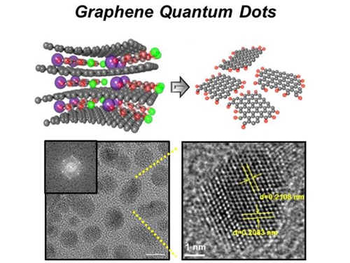
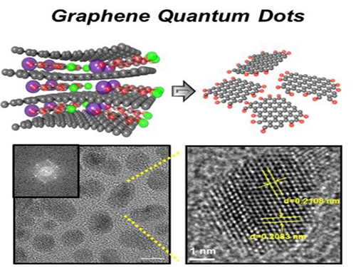 Extracting Light from Graphite: Core Technology of Graphene Quantum Dots Display Developed
Professor Seokwoo Jeon of the Department of Materials Science and Engineering, Professor Yong-Hoon Cho of the Department of Physics, and Professor Seunghyup Yoo of the Department of Electrical Engineering announced that they were able to develop topnotch graphene quantum dots from graphite.
Using the method of synthesizing graphite intercalation compound from graphite with salt and water, the research team developed graphene quantum dots in an ecofriendly way.
The quantum dots have a diameter of 5 nanometers with their sizes equal and yield high quantum efficiency. Unlike conventional quantum dots, they are not comprised of toxic materials such as lead or cadmium. As the quantum dots can be developed from materials which can be easily found in the nature, researchers look forward to putting these into mass production at low cost.
The research team also discovered a luminescence mechanism of graphene quantum dots and confirmed the possibility of commercial use by developing quantum dot light-emitting diodes with brightness of 1,000 cd/m2, which is greater than that of cellphone displays.
Professor Seokwoo Jeon said, “Although quantum dot LEDs have a lower luminous efficiency than existing ones, their luminescent property can be further improved” and emphasized that “using quantum dot displays will allow us to develop not only paper-thin displays but also flexible ones.”
Sponsored by Graphene Research Center in KAIST Institute for NanoCentury, the research finding was published online in the April 20th issue of Advanced Optical Materials.
Picture 1: Graphene quantum dots and their synthesis
Picture 2: Luminescence mechanism of graphene quantum dots
Picture 3: Structure of graphene quantum dots LED and its emission
2014.09.06 View 18738
Extracting Light from Graphite: Core Technology of Graphene Quantum Dots Display Developed
Professor Seokwoo Jeon of the Department of Materials Science and Engineering, Professor Yong-Hoon Cho of the Department of Physics, and Professor Seunghyup Yoo of the Department of Electrical Engineering announced that they were able to develop topnotch graphene quantum dots from graphite.
Using the method of synthesizing graphite intercalation compound from graphite with salt and water, the research team developed graphene quantum dots in an ecofriendly way.
The quantum dots have a diameter of 5 nanometers with their sizes equal and yield high quantum efficiency. Unlike conventional quantum dots, they are not comprised of toxic materials such as lead or cadmium. As the quantum dots can be developed from materials which can be easily found in the nature, researchers look forward to putting these into mass production at low cost.
The research team also discovered a luminescence mechanism of graphene quantum dots and confirmed the possibility of commercial use by developing quantum dot light-emitting diodes with brightness of 1,000 cd/m2, which is greater than that of cellphone displays.
Professor Seokwoo Jeon said, “Although quantum dot LEDs have a lower luminous efficiency than existing ones, their luminescent property can be further improved” and emphasized that “using quantum dot displays will allow us to develop not only paper-thin displays but also flexible ones.”
Sponsored by Graphene Research Center in KAIST Institute for NanoCentury, the research finding was published online in the April 20th issue of Advanced Optical Materials.
Picture 1: Graphene quantum dots and their synthesis
Picture 2: Luminescence mechanism of graphene quantum dots
Picture 3: Structure of graphene quantum dots LED and its emission
2014.09.06 View 18738