School+of+Electrical+Engineering
-
 Is 24-hour health monitoring possible with ambient light energy?
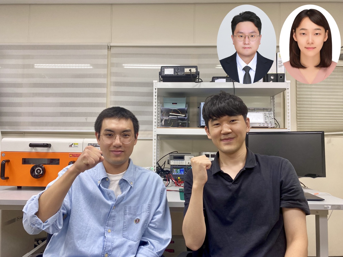
<(From left) Ph.D candidate Youngmin Sim, Ph.D candidate Do Yun Park, Dr. Chanho Park, Professor Kyeongha Kwon>
Miniaturization and weight reduction of medical wearable devices for continuous health monitoring such as heart rate, blood oxygen saturation, and sweat component analysis remain major challenges. In particular, optical sensors consume a significant amount of power for LED operation and wireless transmission, requiring heavy and bulky batteries. To overcome these limitations, KAIST researchers have developed a next-generation wearable platform that enables 24-hour continuous measurement by using ambient light as an energy source and optimizing power management according to the power environment.
KAIST (President Kwang Hyung Lee) announced on the 30th that Professor Kyeongha Kwon's team from the School of Electrical Engineering, in collaboration with Dr. Chanho Park’s team at Northwestern University in the U.S., has developed an adaptive wireless wearable platform that reduces battery load by utilizing ambient light.
To address the battery issue of medical wearable devices, Professor Kyeongha Kwon’s research team developed an innovative platform that utilizes ambient natural light as an energy source. This platform integrates three complementary light energy technologies.
<Figure1.The wireless wearable platform minimizes the energy required for light sources through i) Photometric system that directly utilizes ambient light passing through windows for measurements, ii) Photovoltaic system that receives power from high-efficiency photovoltaic cells and wireless power receiver coils, and iii) Photoluminescent system that stores light using photoluminescent materials and emits light in dark conditions to support the two aforementioned systems. In-sensor computing minimizes power consumption by wirelessly transmitting only essential data. The adaptive power management system efficiently manages power by automatically selecting the optimal mode among 11 different power modes through a power selector based on the power supply level from the photovoltaic system and battery charge status.>
The first core technology, the Photometric Method, is a technique that adaptively adjusts LED brightness depending on the intensity of the ambient light source. By combining ambient natural light with LED light to maintain a constant total illumination level, it automatically dims the LED when natural light is strong and brightens it when natural light is weak.
Whereas conventional sensors had to keep the LED on at a fixed brightness regardless of the environment, this technology optimizes LED power in real time according to the surrounding environment. Experimental results showed that it reduced power consumption by as much as 86.22% under sufficient lighting conditions.
The second is the Photovoltaic Method using high-efficiency multijunction solar cells. This goes beyond simple solar power generation to convert light in both indoor and outdoor environments into electricity. In particular, the adaptive power management system automatically switches among 11 different power configurations based on ambient conditions and battery status to achieve optimal energy efficiency.
The third innovative technology is the Photoluminescent Method. By mixing strontium aluminate microparticles* into the sensor’s silicone encapsulation structure, light from the surroundings is absorbed and stored during the day and slowly released in the dark. As a result, after being exposed to 500W/m² of sunlight for 10 minutes, continuous measurement is possible for 2.5 minutes even in complete darkness.
*Strontium aluminate microparticles: A photoluminescent material used in glow-in-the-dark paint or safety signs, which absorbs light and emits it in the dark for an extended time.
These three technologies work complementarily—during bright conditions, the first and second methods are active, and in dark conditions, the third method provides additional support—enabling 24-hour continuous operation.
The research team applied this platform to various medical sensors to verify its practicality. The photoplethysmography sensor monitors heart rate and blood oxygen saturation in real time, allowing early detection of cardiovascular diseases. The blue light dosimeter accurately measures blue light, which causes skin aging and damage, and provides personalized skin protection guidance. The sweat analysis sensor uses microfluidic technology to simultaneously analyze salt, glucose, and pH in sweat, enabling real-time detection of dehydration and electrolyte imbalances.
Additionally, introducing in-sensor data computing significantly reduced wireless communication power consumption. Previously, all raw data had to be transmitted externally, but now only the necessary results are calculated and transmitted within the sensor, reducing data transmission requirements from 400B/s to 4B/s—a 100-fold decrease.
To validate performance, the research tested the device on healthy adult subjects in four different environments: bright indoor lighting, dim lighting, infrared lighting, and complete darkness. The results showed measurement accuracy equivalent to that of commercial medical devices in all conditions A mouse model experiment confirmed accurate blood oxygen saturation measurement in hypoxic conditions.
<Frigure2.The multimodal device applying the energy harvesting and power management platform consists of i) photoplethysmography (PPG) sensor, ii) blue light dosimeter, iii) photoluminescent microfluidic channel for sweat analysis and biomarker sensors (chloride ion, glucose, and pH), and iv) temperature sensor. This device was implemented with flexible printed circuit board (fPCB) to enable attachment to the skin. A silicon substrate with a window that allows ambient light and measurement light to pass through, along with photoluminescent encapsulation layer, encapsulates the PPG, blue light dosimeter, and temperature sensors, while the photoluminescent microfluidic channel is attached below the photoluminescent encapsulation layer to collect sweat>
Professor Kyeongha Kwon of KAIST, who led the research, stated, “This technology will enable 24-hour continuous health monitoring, shifting the medical paradigm from treatment-centered to prevention-centered shifting the medical paradigm from treatment-centered to prevention-centered,” further stating that “cost savings through early diagnosis as well as strengthened technological competitiveness in the next-generation wearable healthcare market are anticipated.”
This research was published on July 1 in the international journal Nature Communications, with Do Yun Park, a doctoral student in the AI Semiconductor Graduate Program, as co–first author.
※ Paper title: Adaptive Electronics for Photovoltaic, Photoluminescent and Photometric Methods in Power Harvesting for Wireless and Wearable Sensors ※ DOI: https://doi.org/10.1038/s41467-025-60911-1 ※ URL: https://www.nature.com/articles/s41467-025-60911-1
This research was supported by the National Research Foundation of Korea (Outstanding Young Researcher Program and Regional Innovation Leading Research Center Project), the Ministry of Science and ICT and Institute of Information & Communications Technology Planning & Evaluation (IITP) AI Semiconductor Graduate Program, and the BK FOUR Program (Connected AI Education & Research Program for Industry and Society Innovation, KAIST EE).
2025.07.30 View 426
Is 24-hour health monitoring possible with ambient light energy?
<(From left) Ph.D candidate Youngmin Sim, Ph.D candidate Do Yun Park, Dr. Chanho Park, Professor Kyeongha Kwon>
Miniaturization and weight reduction of medical wearable devices for continuous health monitoring such as heart rate, blood oxygen saturation, and sweat component analysis remain major challenges. In particular, optical sensors consume a significant amount of power for LED operation and wireless transmission, requiring heavy and bulky batteries. To overcome these limitations, KAIST researchers have developed a next-generation wearable platform that enables 24-hour continuous measurement by using ambient light as an energy source and optimizing power management according to the power environment.
KAIST (President Kwang Hyung Lee) announced on the 30th that Professor Kyeongha Kwon's team from the School of Electrical Engineering, in collaboration with Dr. Chanho Park’s team at Northwestern University in the U.S., has developed an adaptive wireless wearable platform that reduces battery load by utilizing ambient light.
To address the battery issue of medical wearable devices, Professor Kyeongha Kwon’s research team developed an innovative platform that utilizes ambient natural light as an energy source. This platform integrates three complementary light energy technologies.
<Figure1.The wireless wearable platform minimizes the energy required for light sources through i) Photometric system that directly utilizes ambient light passing through windows for measurements, ii) Photovoltaic system that receives power from high-efficiency photovoltaic cells and wireless power receiver coils, and iii) Photoluminescent system that stores light using photoluminescent materials and emits light in dark conditions to support the two aforementioned systems. In-sensor computing minimizes power consumption by wirelessly transmitting only essential data. The adaptive power management system efficiently manages power by automatically selecting the optimal mode among 11 different power modes through a power selector based on the power supply level from the photovoltaic system and battery charge status.>
The first core technology, the Photometric Method, is a technique that adaptively adjusts LED brightness depending on the intensity of the ambient light source. By combining ambient natural light with LED light to maintain a constant total illumination level, it automatically dims the LED when natural light is strong and brightens it when natural light is weak.
Whereas conventional sensors had to keep the LED on at a fixed brightness regardless of the environment, this technology optimizes LED power in real time according to the surrounding environment. Experimental results showed that it reduced power consumption by as much as 86.22% under sufficient lighting conditions.
The second is the Photovoltaic Method using high-efficiency multijunction solar cells. This goes beyond simple solar power generation to convert light in both indoor and outdoor environments into electricity. In particular, the adaptive power management system automatically switches among 11 different power configurations based on ambient conditions and battery status to achieve optimal energy efficiency.
The third innovative technology is the Photoluminescent Method. By mixing strontium aluminate microparticles* into the sensor’s silicone encapsulation structure, light from the surroundings is absorbed and stored during the day and slowly released in the dark. As a result, after being exposed to 500W/m² of sunlight for 10 minutes, continuous measurement is possible for 2.5 minutes even in complete darkness.
*Strontium aluminate microparticles: A photoluminescent material used in glow-in-the-dark paint or safety signs, which absorbs light and emits it in the dark for an extended time.
These three technologies work complementarily—during bright conditions, the first and second methods are active, and in dark conditions, the third method provides additional support—enabling 24-hour continuous operation.
The research team applied this platform to various medical sensors to verify its practicality. The photoplethysmography sensor monitors heart rate and blood oxygen saturation in real time, allowing early detection of cardiovascular diseases. The blue light dosimeter accurately measures blue light, which causes skin aging and damage, and provides personalized skin protection guidance. The sweat analysis sensor uses microfluidic technology to simultaneously analyze salt, glucose, and pH in sweat, enabling real-time detection of dehydration and electrolyte imbalances.
Additionally, introducing in-sensor data computing significantly reduced wireless communication power consumption. Previously, all raw data had to be transmitted externally, but now only the necessary results are calculated and transmitted within the sensor, reducing data transmission requirements from 400B/s to 4B/s—a 100-fold decrease.
To validate performance, the research tested the device on healthy adult subjects in four different environments: bright indoor lighting, dim lighting, infrared lighting, and complete darkness. The results showed measurement accuracy equivalent to that of commercial medical devices in all conditions A mouse model experiment confirmed accurate blood oxygen saturation measurement in hypoxic conditions.
<Frigure2.The multimodal device applying the energy harvesting and power management platform consists of i) photoplethysmography (PPG) sensor, ii) blue light dosimeter, iii) photoluminescent microfluidic channel for sweat analysis and biomarker sensors (chloride ion, glucose, and pH), and iv) temperature sensor. This device was implemented with flexible printed circuit board (fPCB) to enable attachment to the skin. A silicon substrate with a window that allows ambient light and measurement light to pass through, along with photoluminescent encapsulation layer, encapsulates the PPG, blue light dosimeter, and temperature sensors, while the photoluminescent microfluidic channel is attached below the photoluminescent encapsulation layer to collect sweat>
Professor Kyeongha Kwon of KAIST, who led the research, stated, “This technology will enable 24-hour continuous health monitoring, shifting the medical paradigm from treatment-centered to prevention-centered shifting the medical paradigm from treatment-centered to prevention-centered,” further stating that “cost savings through early diagnosis as well as strengthened technological competitiveness in the next-generation wearable healthcare market are anticipated.”
This research was published on July 1 in the international journal Nature Communications, with Do Yun Park, a doctoral student in the AI Semiconductor Graduate Program, as co–first author.
※ Paper title: Adaptive Electronics for Photovoltaic, Photoluminescent and Photometric Methods in Power Harvesting for Wireless and Wearable Sensors ※ DOI: https://doi.org/10.1038/s41467-025-60911-1 ※ URL: https://www.nature.com/articles/s41467-025-60911-1
This research was supported by the National Research Foundation of Korea (Outstanding Young Researcher Program and Regional Innovation Leading Research Center Project), the Ministry of Science and ICT and Institute of Information & Communications Technology Planning & Evaluation (IITP) AI Semiconductor Graduate Program, and the BK FOUR Program (Connected AI Education & Research Program for Industry and Society Innovation, KAIST EE).
2025.07.30 View 426 -
 Vulnerability Found: One Packet Can Paralyze Smartphones
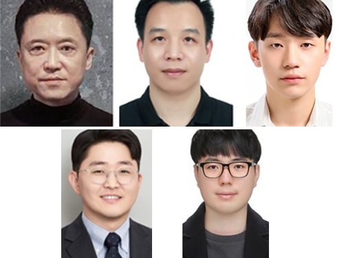
<(From left) Professor Yongdae Kim, PhD candidate Tuan Dinh Hoang, PhD candidate Taekkyung Oh from KAIST, Professor CheolJun Park from Kyung Hee University; and Professor Insu Yun from KAIST>
Smartphones must stay connected to mobile networks at all times to function properly. The core component that enables this constant connectivity is the communication modem (Baseband) inside the device. KAIST researchers, using their self-developed testing framework called 'LLFuzz (Lower Layer Fuzz),' have discovered security vulnerabilities in the lower layers of smartphone communication modems and demonstrated the necessity of standardizing 'mobile communication modem security testing.'
*Standardization: In mobile communication, conformance testing, which verifies normal operation in normal situations, has been standardized. However, standards for handling abnormal packets have not yet been established, hence the need for standardized security testing.
Professor Yongdae Kim's team from the School of Electrical Engineering at KAIST, in a joint research effort with Professor CheolJun Park's team from Kyung Hee University, announced on the 25th of July that they have discovered critical security vulnerabilities in the lower layers of smartphone communication modems. These vulnerabilities can incapacitate smartphone communication with just a single manipulated wireless packet (a data transmission unit in a network). In particular, these vulnerabilities are extremely severe as they can potentially lead to remote code execution (RCE)
The research team utilized their self-developed 'LLFuzz' analysis framework to analyze the lower layer state transitions and error handling logic of the modem to detect security vulnerabilities. LLFuzz was able to precisely extract vulnerabilities caused by implementation errors by comparing and analyzing 3GPP* standard-based state machines with actual device responses.
*3GPP: An international collaborative organization that creates global mobile communication standards.
The research team conducted experiments on 15 commercial smartphones from global manufacturers, including Apple, Samsung Electronics, Google, and Xiaomi, and discovered a total of 11 vulnerabilities. Among these, seven were assigned official CVE (Common Vulnerabilities and Exposures) numbers, and manufacturers applied security patches for these vulnerabilities. However, the remaining four have not yet been publicly disclosed.
While previous security research primarily focused on higher layers of mobile communication, such as NAS (Network Access Stratum) and RRC (Radio Resource Control), the research team concentrated on analyzing the error handling logic of mobile communication's lower layers, which manufacturers have often neglected.
These vulnerabilities occurred in the lower layers of the communication modem (RLC, MAC, PDCP, PHY*), and due to their structural characteristics where encryption or authentication is not applied, operational errors could be induced simply by injecting external signals.
*RLC, MAC, PDCP, PHY: Lower layers of LTE/5G communication, responsible for wireless resource allocation, error control, encryption, and physical layer transmission.
The research team released a demo video showing that when they injected a manipulated wireless packet (malformed MAC packet) into commercial smartphones via a Software-Defined Radio (SDR) device using packets generated on an experimental laptop, the smartphone's communication modem (Baseband) immediately crashed
※ Experiment video: https://drive.google.com/file/d/1NOwZdu_Hf4ScG7LkwgEkHLa_nSV4FPb_/view?usp=drive_link
The video shows data being normally transmitted at 23MB per second on the fast.com page, but immediately after the manipulated packet is injected, the transmission stops and the mobile communication signal disappears. This intuitively demonstrates that a single wireless packet can cripple a commercial device's communication modem.
The vulnerabilities were found in the 'modem chip,' a core component of smartphones responsible for calls, texts, and data communication, making it a very important component.
Qualcomm: Affects over 90 chipsets, including CVE-2025-21477, CVE-2024-23385.
MediaTek: Affects over 80 chipsets, including CVE-2024-20076, CVE-2024-20077, CVE-2025-20659.
Samsung: CVE-2025-26780 (targets the latest chipsets like Exynos 2400, 5400).
Apple: CVE-2024-27870 (shares the same vulnerability as Qualcomm CVE).
The problematic modem chips (communication components) are not only in premium smartphones but also in low-end smartphones, tablets, smartwatches, and IoT devices, leading to the widespread potential for user harm due to their broad diffusion.
Furthermore, the research team experimentally tested 5G vulnerabilities in the lower layers and found two vulnerabilities in just two weeks. Considering that 5G vulnerability checks have not been generally conducted, it is possible that many more vulnerabilities exist in the mobile communication lower layers of baseband chips.
Professor Yongdae Kim explained, "The lower layers of smartphone communication modems are not subject to encryption or authentication, creating a structural risk where devices can accept arbitrary signals from external sources." He added, "This research demonstrates the necessity of standardizing mobile communication modem security testing for smartphones and other IoT devices."
The research team is continuing additional analysis of the 5G lower layers using LLFuzz and is also developing tools for testing LTE and 5G upper layers. They are also pursuing collaborations for future tool disclosure. The team's stance is that "as technological complexity increases, systemic security inspection systems must evolve in parallel."
First author Tuan Dinh Hoang, a Ph.D. student in the School of Electrical Engineering, will present the research results in August at USENIX Security 2025, one of the world's most prestigious conferences in cybersecurity.
※ Paper Title: LLFuzz: An Over-the-Air Dynamic Testing Framework for Cellular Baseband Lower Layers (Tuan Dinh Hoang and Taekkyung Oh, KAIST; CheolJun Park, Kyung Hee Univ.; Insu Yun and Yongdae Kim, KAIST)
※ Usenix paper site: https://www.usenix.org/conference/usenixsecurity25/presentation/hoang (Not yet public), Lab homepage paper: https://syssec.kaist.ac.kr/pub/2025/LLFuzz_Tuan.pdf
※ Open-source repository: https://github.com/SysSec-KAIST/LLFuzz (To be released)
This research was conducted with support from the Institute of Information & Communications Technology Planning & Evaluation (IITP) funded by the Ministry of Science and ICT.
2025.07.25 View 548
Vulnerability Found: One Packet Can Paralyze Smartphones
<(From left) Professor Yongdae Kim, PhD candidate Tuan Dinh Hoang, PhD candidate Taekkyung Oh from KAIST, Professor CheolJun Park from Kyung Hee University; and Professor Insu Yun from KAIST>
Smartphones must stay connected to mobile networks at all times to function properly. The core component that enables this constant connectivity is the communication modem (Baseband) inside the device. KAIST researchers, using their self-developed testing framework called 'LLFuzz (Lower Layer Fuzz),' have discovered security vulnerabilities in the lower layers of smartphone communication modems and demonstrated the necessity of standardizing 'mobile communication modem security testing.'
*Standardization: In mobile communication, conformance testing, which verifies normal operation in normal situations, has been standardized. However, standards for handling abnormal packets have not yet been established, hence the need for standardized security testing.
Professor Yongdae Kim's team from the School of Electrical Engineering at KAIST, in a joint research effort with Professor CheolJun Park's team from Kyung Hee University, announced on the 25th of July that they have discovered critical security vulnerabilities in the lower layers of smartphone communication modems. These vulnerabilities can incapacitate smartphone communication with just a single manipulated wireless packet (a data transmission unit in a network). In particular, these vulnerabilities are extremely severe as they can potentially lead to remote code execution (RCE)
The research team utilized their self-developed 'LLFuzz' analysis framework to analyze the lower layer state transitions and error handling logic of the modem to detect security vulnerabilities. LLFuzz was able to precisely extract vulnerabilities caused by implementation errors by comparing and analyzing 3GPP* standard-based state machines with actual device responses.
*3GPP: An international collaborative organization that creates global mobile communication standards.
The research team conducted experiments on 15 commercial smartphones from global manufacturers, including Apple, Samsung Electronics, Google, and Xiaomi, and discovered a total of 11 vulnerabilities. Among these, seven were assigned official CVE (Common Vulnerabilities and Exposures) numbers, and manufacturers applied security patches for these vulnerabilities. However, the remaining four have not yet been publicly disclosed.
While previous security research primarily focused on higher layers of mobile communication, such as NAS (Network Access Stratum) and RRC (Radio Resource Control), the research team concentrated on analyzing the error handling logic of mobile communication's lower layers, which manufacturers have often neglected.
These vulnerabilities occurred in the lower layers of the communication modem (RLC, MAC, PDCP, PHY*), and due to their structural characteristics where encryption or authentication is not applied, operational errors could be induced simply by injecting external signals.
*RLC, MAC, PDCP, PHY: Lower layers of LTE/5G communication, responsible for wireless resource allocation, error control, encryption, and physical layer transmission.
The research team released a demo video showing that when they injected a manipulated wireless packet (malformed MAC packet) into commercial smartphones via a Software-Defined Radio (SDR) device using packets generated on an experimental laptop, the smartphone's communication modem (Baseband) immediately crashed
※ Experiment video: https://drive.google.com/file/d/1NOwZdu_Hf4ScG7LkwgEkHLa_nSV4FPb_/view?usp=drive_link
The video shows data being normally transmitted at 23MB per second on the fast.com page, but immediately after the manipulated packet is injected, the transmission stops and the mobile communication signal disappears. This intuitively demonstrates that a single wireless packet can cripple a commercial device's communication modem.
The vulnerabilities were found in the 'modem chip,' a core component of smartphones responsible for calls, texts, and data communication, making it a very important component.
Qualcomm: Affects over 90 chipsets, including CVE-2025-21477, CVE-2024-23385.
MediaTek: Affects over 80 chipsets, including CVE-2024-20076, CVE-2024-20077, CVE-2025-20659.
Samsung: CVE-2025-26780 (targets the latest chipsets like Exynos 2400, 5400).
Apple: CVE-2024-27870 (shares the same vulnerability as Qualcomm CVE).
The problematic modem chips (communication components) are not only in premium smartphones but also in low-end smartphones, tablets, smartwatches, and IoT devices, leading to the widespread potential for user harm due to their broad diffusion.
Furthermore, the research team experimentally tested 5G vulnerabilities in the lower layers and found two vulnerabilities in just two weeks. Considering that 5G vulnerability checks have not been generally conducted, it is possible that many more vulnerabilities exist in the mobile communication lower layers of baseband chips.
Professor Yongdae Kim explained, "The lower layers of smartphone communication modems are not subject to encryption or authentication, creating a structural risk where devices can accept arbitrary signals from external sources." He added, "This research demonstrates the necessity of standardizing mobile communication modem security testing for smartphones and other IoT devices."
The research team is continuing additional analysis of the 5G lower layers using LLFuzz and is also developing tools for testing LTE and 5G upper layers. They are also pursuing collaborations for future tool disclosure. The team's stance is that "as technological complexity increases, systemic security inspection systems must evolve in parallel."
First author Tuan Dinh Hoang, a Ph.D. student in the School of Electrical Engineering, will present the research results in August at USENIX Security 2025, one of the world's most prestigious conferences in cybersecurity.
※ Paper Title: LLFuzz: An Over-the-Air Dynamic Testing Framework for Cellular Baseband Lower Layers (Tuan Dinh Hoang and Taekkyung Oh, KAIST; CheolJun Park, Kyung Hee Univ.; Insu Yun and Yongdae Kim, KAIST)
※ Usenix paper site: https://www.usenix.org/conference/usenixsecurity25/presentation/hoang (Not yet public), Lab homepage paper: https://syssec.kaist.ac.kr/pub/2025/LLFuzz_Tuan.pdf
※ Open-source repository: https://github.com/SysSec-KAIST/LLFuzz (To be released)
This research was conducted with support from the Institute of Information & Communications Technology Planning & Evaluation (IITP) funded by the Ministry of Science and ICT.
2025.07.25 View 548 -
 KAIST Presents Game-Changing Technology for Intractable Brain Disease Treatment Using Micro OLEDs
<(From left)Professor Kyung Cheol Choi, Professor Hyunjoo J. Lee, Dr. Somin Lee from the School of Electrical Engineering>
Optogenetics is a technique that controls neural activity by stimulating neurons expressing light-sensitive proteins with specific wavelengths of light. It has opened new possibilities for identifying causes of brain disorders and developing treatments for intractable neurological diseases. Because this technology requires precise stimulation inside the human brain with minimal damage to soft brain tissue, it must be integrated into a neural probe—a medical device implanted in the brain. KAIST researchers have now proposed a new paradigm for neural probes by integrating micro OLEDs into thin, flexible, implantable medical devices.
KAIST (President Kwang Hyung Lee) announced on the 6th of July that professor Kyung Cheol Choi and professor Hyunjoo J. Lee from the School of Electrical Engineering have jointly succeeded in developing an optogenetic neural probe integrated with flexible micro OLEDs.
Optical fibers have been used for decades in optogenetic research to deliver light to deep brain regions from external light sources. Recently, research has focused on flexible optical fibers and ultra-miniaturized neural probes that integrate light sources for single-neuron stimulation.
The research team focused on micro OLEDs due to their high spatial resolution and flexibility, which allow for precise light delivery to small areas of neurons. This enables detailed brain circuit analysis while minimizing side effects and avoiding restrictions on animal movement. Moreover, micro OLEDs offer precise control of light wavelengths and support multi-site stimulation, making them suitable for studying complex brain functions.
However, the device's electrical properties degrade easily in the presence of moisture or water, which limited their use as implantable bioelectronics. Furthermore, optimizing the high-resolution integration process on thin, flexible probes remained a challenge.
To address this, the team enhanced the operational reliability of OLEDs in moist, oxygen-rich environments and minimized tissue damage during implantation. They patterned an ultrathin, flexible encapsulation layer* composed of aluminum oxide and parylene-C (Al₂O₃/parylene-C) at widths of 260–600 micrometers (μm) to maintain biocompatibility.
*Encapsulation layer: A barrier that completely blocks oxygen and water molecules from the external environment, ensuring the longevity and reliability of the device.
When integrating the high-resolution micro OLEDs, the researchers also used parylene-C, the same biocompatible material as the encapsulation layer, to maintain flexibility and safety. To eliminate electrical interference between adjacent OLED pixels and spatially separate them, they introduced a pixel define layer (PDL), enabling the independent operation of eight micro OLEDs.
Furthermore, they precisely controlled the residual stress and thickness in the multilayer film structure of the device, ensuring its flexibility even in biological environments. This optimization allowed for probe insertion without bending or external shuttles or needles, minimizing mechanical stress during implantation.
2025.07.07 View 698
KAIST Presents Game-Changing Technology for Intractable Brain Disease Treatment Using Micro OLEDs
<(From left)Professor Kyung Cheol Choi, Professor Hyunjoo J. Lee, Dr. Somin Lee from the School of Electrical Engineering>
Optogenetics is a technique that controls neural activity by stimulating neurons expressing light-sensitive proteins with specific wavelengths of light. It has opened new possibilities for identifying causes of brain disorders and developing treatments for intractable neurological diseases. Because this technology requires precise stimulation inside the human brain with minimal damage to soft brain tissue, it must be integrated into a neural probe—a medical device implanted in the brain. KAIST researchers have now proposed a new paradigm for neural probes by integrating micro OLEDs into thin, flexible, implantable medical devices.
KAIST (President Kwang Hyung Lee) announced on the 6th of July that professor Kyung Cheol Choi and professor Hyunjoo J. Lee from the School of Electrical Engineering have jointly succeeded in developing an optogenetic neural probe integrated with flexible micro OLEDs.
Optical fibers have been used for decades in optogenetic research to deliver light to deep brain regions from external light sources. Recently, research has focused on flexible optical fibers and ultra-miniaturized neural probes that integrate light sources for single-neuron stimulation.
The research team focused on micro OLEDs due to their high spatial resolution and flexibility, which allow for precise light delivery to small areas of neurons. This enables detailed brain circuit analysis while minimizing side effects and avoiding restrictions on animal movement. Moreover, micro OLEDs offer precise control of light wavelengths and support multi-site stimulation, making them suitable for studying complex brain functions.
However, the device's electrical properties degrade easily in the presence of moisture or water, which limited their use as implantable bioelectronics. Furthermore, optimizing the high-resolution integration process on thin, flexible probes remained a challenge.
To address this, the team enhanced the operational reliability of OLEDs in moist, oxygen-rich environments and minimized tissue damage during implantation. They patterned an ultrathin, flexible encapsulation layer* composed of aluminum oxide and parylene-C (Al₂O₃/parylene-C) at widths of 260–600 micrometers (μm) to maintain biocompatibility.
*Encapsulation layer: A barrier that completely blocks oxygen and water molecules from the external environment, ensuring the longevity and reliability of the device.
When integrating the high-resolution micro OLEDs, the researchers also used parylene-C, the same biocompatible material as the encapsulation layer, to maintain flexibility and safety. To eliminate electrical interference between adjacent OLED pixels and spatially separate them, they introduced a pixel define layer (PDL), enabling the independent operation of eight micro OLEDs.
Furthermore, they precisely controlled the residual stress and thickness in the multilayer film structure of the device, ensuring its flexibility even in biological environments. This optimization allowed for probe insertion without bending or external shuttles or needles, minimizing mechanical stress during implantation.
2025.07.07 View 698 -
 Manipulating Brain Cells by Smartphone
Researchers have developed a soft neural implant that can be wirelessly controlled using a smartphone. It is the first wireless neural device capable of indefinitely delivering multiple drugs and multiple colour lights, which neuroscientists believe can speed up efforts to uncover brain diseases such as Parkinson’s, Alzheimer’s, addiction, depression, and pain.
A team under Professor Jae-Woong Jeong from the School of Electrical Engineering at KAIST and his collaborators have invented a device that can control neural circuits using a tiny brain implant controlled by a smartphone. The device, using Lego-like replaceable drug cartridges and powerful, low-energy Bluetooth, can target specific neurons of interest using drugs and light for prolonged periods. This study was published in Nature Biomedical Engineering.
“This novel device is the fruit of advanced electronics design and powerful micro and nanoscale engineering,” explained Professor Jeong. “We are interested in further developing this technology to make a brain implant for clinical applications.”
This technology significantly overshadows the conventional methods used by neuroscientists, which usually involve rigid metal tubes and optical fibers to deliver drugs and light. Apart from limiting the subject’s movement due to bulky equipment, their relatively rigid structure causes lesions in soft brain tissue over time, therefore making them not suitable for long-term implantation. Although some efforts have been made to partly mitigate adverse tissue response by incorporating soft probes and wireless platforms, the previous solutions were limited by their inability to deliver drugs for long periods of time as well as their bulky and complex control setups.
To achieve chronic wireless drug delivery, scientists had to solve the critical challenge of the exhaustion and evaporation of drugs. To combat this, the researchers invented a neural device with a replaceable drug cartridge, which could allow neuroscientists to study the same brain circuits for several months without worrying about running out of drugs.
These ‘plug-n-play’ drug cartridges were assembled into a brain implant for mice with a soft and ultrathin probe (with the thickness of a human hair), which consisted of microfluidic channels and tiny LEDs (smaller than a grain of salt), for unlimited drug doses and light delivery.
Controlled with an elegant and simple user interface on a smartphone, neuroscientists can easily trigger any specific combination or precise sequencing of light and drug delivery in any implanted target animal without the need to be physically inside the laboratory. Using these wireless neural devices, researchers can also easily setup fully automated animal studies where the behaviour of one animal could affect other animals by triggering light and/or drug delivery.
“The wireless neural device enables chronic chemical and optical neuromodulation that has never been achieved before,” said lead author Raza Qazi, a researcher with KAIST and the University of Colorado Boulder.
This work was supported by grants from the National Research Foundation of Korea, US National Institute of Health, National Institute on Drug Abuse, and Mallinckrodt Professorship.
(A neural implant with replaceable drug cartridges and Bluetooth low-energy can target specific neurons .)
(Micro LED controlling using smartphone application)
2019.08.07 View 35230
Manipulating Brain Cells by Smartphone
Researchers have developed a soft neural implant that can be wirelessly controlled using a smartphone. It is the first wireless neural device capable of indefinitely delivering multiple drugs and multiple colour lights, which neuroscientists believe can speed up efforts to uncover brain diseases such as Parkinson’s, Alzheimer’s, addiction, depression, and pain.
A team under Professor Jae-Woong Jeong from the School of Electrical Engineering at KAIST and his collaborators have invented a device that can control neural circuits using a tiny brain implant controlled by a smartphone. The device, using Lego-like replaceable drug cartridges and powerful, low-energy Bluetooth, can target specific neurons of interest using drugs and light for prolonged periods. This study was published in Nature Biomedical Engineering.
“This novel device is the fruit of advanced electronics design and powerful micro and nanoscale engineering,” explained Professor Jeong. “We are interested in further developing this technology to make a brain implant for clinical applications.”
This technology significantly overshadows the conventional methods used by neuroscientists, which usually involve rigid metal tubes and optical fibers to deliver drugs and light. Apart from limiting the subject’s movement due to bulky equipment, their relatively rigid structure causes lesions in soft brain tissue over time, therefore making them not suitable for long-term implantation. Although some efforts have been made to partly mitigate adverse tissue response by incorporating soft probes and wireless platforms, the previous solutions were limited by their inability to deliver drugs for long periods of time as well as their bulky and complex control setups.
To achieve chronic wireless drug delivery, scientists had to solve the critical challenge of the exhaustion and evaporation of drugs. To combat this, the researchers invented a neural device with a replaceable drug cartridge, which could allow neuroscientists to study the same brain circuits for several months without worrying about running out of drugs.
These ‘plug-n-play’ drug cartridges were assembled into a brain implant for mice with a soft and ultrathin probe (with the thickness of a human hair), which consisted of microfluidic channels and tiny LEDs (smaller than a grain of salt), for unlimited drug doses and light delivery.
Controlled with an elegant and simple user interface on a smartphone, neuroscientists can easily trigger any specific combination or precise sequencing of light and drug delivery in any implanted target animal without the need to be physically inside the laboratory. Using these wireless neural devices, researchers can also easily setup fully automated animal studies where the behaviour of one animal could affect other animals by triggering light and/or drug delivery.
“The wireless neural device enables chronic chemical and optical neuromodulation that has never been achieved before,” said lead author Raza Qazi, a researcher with KAIST and the University of Colorado Boulder.
This work was supported by grants from the National Research Foundation of Korea, US National Institute of Health, National Institute on Drug Abuse, and Mallinckrodt Professorship.
(A neural implant with replaceable drug cartridges and Bluetooth low-energy can target specific neurons .)
(Micro LED controlling using smartphone application)
2019.08.07 View 35230 -
 Anti-drone Technology for Anti-Terrorism Applications
(from top right clockwise: Professor Yongdae Kim,
PhD Candidates Yujin Kwon, Juhwan Noh, Hocheol Shin, and Dohyun Kim)
KAIST researchers have developed anti-drone technology that can hijack other drones by spoofing its location using fake GPS signals. This technology can safely guide a drone to a desired location without any sudden change in direction in emergency situations, and thus respond effectively to dangerous drones such as those intending to carry out acts of terrorism.
Advancements in the drone industry have led to the wider use of drones in our daily lives in areas of reconnaissance, searching and rescuing, disaster prevention and response, and delivery services. At the same time, there has also been a growing concern about privacy, safety, and security issues regarding drones, especially those arising from intrusion into private property and secure facilities. Therefore, the anti-drone industry is rapidly expanding to detect and respond to this possible drone invasion.
The current anti-drone systems used in airports and other key locations utilize electronic jamming signals, high-power lasers, or nets to neutralize drones. For example, drones trespassing on airports are often countered with simple jamming signals that can prevent the drones from moving and changing position, but this may result in a prolonged delay in flight departures and arrivals at the airports. Drones used for terrorist attacks – armed with explosives or weapons – must also be neutralized a safe distance from the public and vital infrastructure to minimize any damage.
Due to this need for a new anti-drone technology to counter these threats, a KAIST research team led by Professor Yongdae Kim from the School of Electrical Engineering has developed technology that securely thwarts drones by tricking them with fake GPS signals.
Fake GPS signals have been used in previous studies to cause confusion inside the drone regarding its location, making the drone drift from its position or path. However, such attack tactics cannot be applied in GPS safety mode. GPS safety mode is an emergency mode that ensures drone safety when the signal is cut or location accuracy is low due to a fake GPS signals. This mode differs between models and manufacturers.
Professor Kim’s team analyzed the GPS safety mode of different drone models made from major drone manufacturers such as DJI and Parrot, made classification systems, and designed a drone abduction technique that covers almost all the types of drone GPS safety modes, and is universally applicable to any drone that uses GPS regardless of model or manufacturer. The research team applied their new technique to four different drones and have proven that the drones can be safely hijacked and guided to the direction of intentional abduction within a small margin of error.
Professor Kim said, “Conventional consumer drones equipped with GPS safety mode seem to be safe from fake GPS signals, however, most of these drones are able to be detoured since they detect GPS errors in a rudimentary manner.” He continued, “This technology can contribute particularly to reducing damage to airports and the airline industry caused by illegal drone flights.”
The research team is planning to commercialize the developed technology by applying it to existing anti-drone solutions through technology transfer.” This research, featured in the ACM Transactions on Privacy and Security (TOPS) on April 9, was supported by the Defense Acquisition Program Administration (DAPA) and the Agency for Defense Development (ADD).
Image 1.
Experimental environment in which a fake GPS signal was produced from a PC and injected into the drone signal using directional antennae
Publication:
Juhwan Noh, Yujin Kwon, Yunmok Son, Hocheol Shin, Dohyun Kim, Jaeyeong Choi, and Yongdae Kim. 2019. Tractor Beam: Safe-hijacking of Consumer Drones with Adaptive GPS Spoofing. ACM Transactions on Privacy and Security. New York, NY, USA, Vol. 22, No. 2, Article 12, 26 pages. https://doi.org/10.1145/3309735
Profile: Prof. Yongdae Kim, MS, PhD
yongdaek@kaist.ac.kr
https://www.syssec.kr/
Professor
School of Electrical Engineering
Korea Advanced Institute of Science and Technology (KAIST)
http://kaist.ac.kr Daejeon 34141, Korea
Profile: Juhwan Noh, PhD Candidate
juhwan@kaist.ac.kr
PhD Candidate
System Security (SysSec) Lab
School of Electrical Engineering
Korea Advanced Institute of Science and Technology (KAIST)
http://kaist.ac.kr Daejeon 34141, Korea
(END)
2019.06.25 View 46356
Anti-drone Technology for Anti-Terrorism Applications
(from top right clockwise: Professor Yongdae Kim,
PhD Candidates Yujin Kwon, Juhwan Noh, Hocheol Shin, and Dohyun Kim)
KAIST researchers have developed anti-drone technology that can hijack other drones by spoofing its location using fake GPS signals. This technology can safely guide a drone to a desired location without any sudden change in direction in emergency situations, and thus respond effectively to dangerous drones such as those intending to carry out acts of terrorism.
Advancements in the drone industry have led to the wider use of drones in our daily lives in areas of reconnaissance, searching and rescuing, disaster prevention and response, and delivery services. At the same time, there has also been a growing concern about privacy, safety, and security issues regarding drones, especially those arising from intrusion into private property and secure facilities. Therefore, the anti-drone industry is rapidly expanding to detect and respond to this possible drone invasion.
The current anti-drone systems used in airports and other key locations utilize electronic jamming signals, high-power lasers, or nets to neutralize drones. For example, drones trespassing on airports are often countered with simple jamming signals that can prevent the drones from moving and changing position, but this may result in a prolonged delay in flight departures and arrivals at the airports. Drones used for terrorist attacks – armed with explosives or weapons – must also be neutralized a safe distance from the public and vital infrastructure to minimize any damage.
Due to this need for a new anti-drone technology to counter these threats, a KAIST research team led by Professor Yongdae Kim from the School of Electrical Engineering has developed technology that securely thwarts drones by tricking them with fake GPS signals.
Fake GPS signals have been used in previous studies to cause confusion inside the drone regarding its location, making the drone drift from its position or path. However, such attack tactics cannot be applied in GPS safety mode. GPS safety mode is an emergency mode that ensures drone safety when the signal is cut or location accuracy is low due to a fake GPS signals. This mode differs between models and manufacturers.
Professor Kim’s team analyzed the GPS safety mode of different drone models made from major drone manufacturers such as DJI and Parrot, made classification systems, and designed a drone abduction technique that covers almost all the types of drone GPS safety modes, and is universally applicable to any drone that uses GPS regardless of model or manufacturer. The research team applied their new technique to four different drones and have proven that the drones can be safely hijacked and guided to the direction of intentional abduction within a small margin of error.
Professor Kim said, “Conventional consumer drones equipped with GPS safety mode seem to be safe from fake GPS signals, however, most of these drones are able to be detoured since they detect GPS errors in a rudimentary manner.” He continued, “This technology can contribute particularly to reducing damage to airports and the airline industry caused by illegal drone flights.”
The research team is planning to commercialize the developed technology by applying it to existing anti-drone solutions through technology transfer.” This research, featured in the ACM Transactions on Privacy and Security (TOPS) on April 9, was supported by the Defense Acquisition Program Administration (DAPA) and the Agency for Defense Development (ADD).
Image 1.
Experimental environment in which a fake GPS signal was produced from a PC and injected into the drone signal using directional antennae
Publication:
Juhwan Noh, Yujin Kwon, Yunmok Son, Hocheol Shin, Dohyun Kim, Jaeyeong Choi, and Yongdae Kim. 2019. Tractor Beam: Safe-hijacking of Consumer Drones with Adaptive GPS Spoofing. ACM Transactions on Privacy and Security. New York, NY, USA, Vol. 22, No. 2, Article 12, 26 pages. https://doi.org/10.1145/3309735
Profile: Prof. Yongdae Kim, MS, PhD
yongdaek@kaist.ac.kr
https://www.syssec.kr/
Professor
School of Electrical Engineering
Korea Advanced Institute of Science and Technology (KAIST)
http://kaist.ac.kr Daejeon 34141, Korea
Profile: Juhwan Noh, PhD Candidate
juhwan@kaist.ac.kr
PhD Candidate
System Security (SysSec) Lab
School of Electrical Engineering
Korea Advanced Institute of Science and Technology (KAIST)
http://kaist.ac.kr Daejeon 34141, Korea
(END)
2019.06.25 View 46356 -
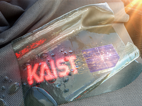 True-meaning Wearable Displays: Self-powered, Washable and Wearable
(Video: The washing process of wearing display module) When we think about clothes, they are usually formed with textiles and have to be both wearable and washable for daily use; however, smart clothing has had a problem with its power sources and moisture permeability, which causes the devices to malfunction. This problem has now been overcome by a KAIST research team, who developed a textile-based wearable display module technology that is washable and does not require an external power source.
To ease out the problem of external power sources and enhance the practicability of wearable displays, Professor Kyung Cheol Choi from the School of Electrical Engineering and his team fabricated their wearing display modules on real textiles that integrated polymer solar cells (PSCs) with organic light emitting diodes (OLEDs).
PSCs have been one of the most promising candidates for a next-generation power source, especially for wearable and optoelectronic applications because they can provide stable power without an external power source, while OLEDs can be driven with milliwatts. However, the problem was that they are both very vulnerable to external moisture and oxygen. The encapsulation barrier is essential for their reliability. The conventional encapsulation barrier is sufficient for normal environments; however, it loses its characteristics in aqueous environments, such as water. It limits the commercialization of wearing displays that must operate even on rainy days or after washing.
To tackle this issue, the team employed a washable encapsulation barrier that can protect the device without losing its characteristics after washing through atomic layer deposition (ALD) and spin coating. With this encapsulation technology, the team confirmed that textile-based wearing display modules including PSCs, OLEDs, and the proposed encapsulation barrier exhibited little change in characteristics even after 20 washings with 10-minute cycles. Moreover, the encapsulated device operated stably with a low curvature radius of 3mm and boasted high reliability.
Finally, it exhibited no deterioration in properties over 30 days even after being subjected to both bending stress and washing. Since it uses a less stressful textile, compared to conventional wearable electronic devices that use traditional plastic substrates, this technology can accelerate the commercialization of wearing electronic devices. Importantly, this wearable electronic device in daily life can save energy through a self-powered system.
Professor Choi said, “I could say that this research realized a truly washable wearable electronic module in the sense that it uses daily wearable textiles instead of the plastic used in conventional wearable electronic devices. Saving energy with PSCs, it can be self-powered, using nature-friendly solar energy, and washed. I believe that it has paved the way for a ‘true-meaning wearable display’ that can be formed on textile, beyond the attachable form of wearable technology.”
This research, in collaboration with Professor Seok Ho Cho from Chonnam National University and led by Eun Gyo Jeong, was published in Energy and Environmental Science (10.1039/c8ee03271h) on January 18, 2019.
Figure 1. Schematic and photo of a washable wearing display module
Figure 2. Cover page of Energy and Environmental Science
2019.03.21 View 32664
True-meaning Wearable Displays: Self-powered, Washable and Wearable
(Video: The washing process of wearing display module) When we think about clothes, they are usually formed with textiles and have to be both wearable and washable for daily use; however, smart clothing has had a problem with its power sources and moisture permeability, which causes the devices to malfunction. This problem has now been overcome by a KAIST research team, who developed a textile-based wearable display module technology that is washable and does not require an external power source.
To ease out the problem of external power sources and enhance the practicability of wearable displays, Professor Kyung Cheol Choi from the School of Electrical Engineering and his team fabricated their wearing display modules on real textiles that integrated polymer solar cells (PSCs) with organic light emitting diodes (OLEDs).
PSCs have been one of the most promising candidates for a next-generation power source, especially for wearable and optoelectronic applications because they can provide stable power without an external power source, while OLEDs can be driven with milliwatts. However, the problem was that they are both very vulnerable to external moisture and oxygen. The encapsulation barrier is essential for their reliability. The conventional encapsulation barrier is sufficient for normal environments; however, it loses its characteristics in aqueous environments, such as water. It limits the commercialization of wearing displays that must operate even on rainy days or after washing.
To tackle this issue, the team employed a washable encapsulation barrier that can protect the device without losing its characteristics after washing through atomic layer deposition (ALD) and spin coating. With this encapsulation technology, the team confirmed that textile-based wearing display modules including PSCs, OLEDs, and the proposed encapsulation barrier exhibited little change in characteristics even after 20 washings with 10-minute cycles. Moreover, the encapsulated device operated stably with a low curvature radius of 3mm and boasted high reliability.
Finally, it exhibited no deterioration in properties over 30 days even after being subjected to both bending stress and washing. Since it uses a less stressful textile, compared to conventional wearable electronic devices that use traditional plastic substrates, this technology can accelerate the commercialization of wearing electronic devices. Importantly, this wearable electronic device in daily life can save energy through a self-powered system.
Professor Choi said, “I could say that this research realized a truly washable wearable electronic module in the sense that it uses daily wearable textiles instead of the plastic used in conventional wearable electronic devices. Saving energy with PSCs, it can be self-powered, using nature-friendly solar energy, and washed. I believe that it has paved the way for a ‘true-meaning wearable display’ that can be formed on textile, beyond the attachable form of wearable technology.”
This research, in collaboration with Professor Seok Ho Cho from Chonnam National University and led by Eun Gyo Jeong, was published in Energy and Environmental Science (10.1039/c8ee03271h) on January 18, 2019.
Figure 1. Schematic and photo of a washable wearing display module
Figure 2. Cover page of Energy and Environmental Science
2019.03.21 View 32664 -
 Wafer-Scale Multilayer Fabrication of Silk Fibroin-Based Microelectronics
A KAIST research team developed a novel fabrication method for the multilayer processing of silk-based microelectronics. This technology for creating a biodegradable silk fibroin film allows microfabrication with polymer or metal structures manufactured from photolithography. It can be a key technology in the implementation of silk fibroin-based biodegradable electronic devices or localized drug delivery through silk fibroin patterns.
Silk fibroins are biocompatible, biodegradable, transparent, and flexible, which makes them excellent candidates for implantable biomedical devices, and they have also been used as biodegradable films and functional microstructures in biomedical applications. However, conventional microfabrication processes require strong etching solutions and solvents to modify the structure of silk fibroins.
To prevent the silk fibroin from being damaged during the process, Professor Hyunjoo J. Lee from the School of Electrical Engineering and her team came up with a novel process, named aluminum hard mask on silk fibroin (AMoS), which is capable of micropatterning multiple layers composed of both fibroin and inorganic materials, such as metal and dielectrics with high-precision microscale alignment. The AMoS process can make silk fibroin patterns on devices, or make patterns on silk fibroin thin films with other materials by using photolithography, which is a core technology in the current microfabrication process.
The team successfully cultured primary neurons on the processed silk fibroin micro-patterns, and confirmed that silk fibroin has excellent biocompatibility before and after the fabrication process and that it also can be applied to implanted biological devices.
Through this technology, the team realized the multilayer micropatterning of fibroin films on a silk fibroin substrate and fabricated a biodegradable microelectric circuit consisting of resistors and silk fibroin dielectric capacitors in a silicon wafer with large areas.
They also used this technology to position the micro-pattern of the silk fibroin thin film closer to the flexible polymer-based brain electrode, and confirmed the dye molecules mounted on the silk fibroin were transferred successfully from the micropatterns.
Professor Lee said, “This technology facilitates wafer-scale, large-area processing of sensitive materials. We expect it to be applied to a wide range of biomedical devices in the future. Using the silk fibroin with micro-patterned brain electrodes can open up many new possibilities in research on brain circuits by mounting drugs that restrict or promote brain cell activities.”
This research, in collaboration with Dr. Nakwon Choi from KIST and led by PhD candidate Geon Kook, was published in ACS AMI (10.1021/acsami.8b13170) on January 16, 2019.
Figure 1. The cover page of ACS AMI
Figure 2. Fibroin microstructures and metal patterns on a fibroin produced by using the AMoS mask.
Figure 3. Biocompatibility assessment of the AMoS Process. Top: Schematics image of a) fibroin-coated silicon b) fibroin-pattered silicon and c) gold-patterned fibroin. Bottom: Representative confocal microscopy images of live (green) and dead (red) primary cortical neurons cultured on the substrates.
2019.03.15 View 23889
Wafer-Scale Multilayer Fabrication of Silk Fibroin-Based Microelectronics
A KAIST research team developed a novel fabrication method for the multilayer processing of silk-based microelectronics. This technology for creating a biodegradable silk fibroin film allows microfabrication with polymer or metal structures manufactured from photolithography. It can be a key technology in the implementation of silk fibroin-based biodegradable electronic devices or localized drug delivery through silk fibroin patterns.
Silk fibroins are biocompatible, biodegradable, transparent, and flexible, which makes them excellent candidates for implantable biomedical devices, and they have also been used as biodegradable films and functional microstructures in biomedical applications. However, conventional microfabrication processes require strong etching solutions and solvents to modify the structure of silk fibroins.
To prevent the silk fibroin from being damaged during the process, Professor Hyunjoo J. Lee from the School of Electrical Engineering and her team came up with a novel process, named aluminum hard mask on silk fibroin (AMoS), which is capable of micropatterning multiple layers composed of both fibroin and inorganic materials, such as metal and dielectrics with high-precision microscale alignment. The AMoS process can make silk fibroin patterns on devices, or make patterns on silk fibroin thin films with other materials by using photolithography, which is a core technology in the current microfabrication process.
The team successfully cultured primary neurons on the processed silk fibroin micro-patterns, and confirmed that silk fibroin has excellent biocompatibility before and after the fabrication process and that it also can be applied to implanted biological devices.
Through this technology, the team realized the multilayer micropatterning of fibroin films on a silk fibroin substrate and fabricated a biodegradable microelectric circuit consisting of resistors and silk fibroin dielectric capacitors in a silicon wafer with large areas.
They also used this technology to position the micro-pattern of the silk fibroin thin film closer to the flexible polymer-based brain electrode, and confirmed the dye molecules mounted on the silk fibroin were transferred successfully from the micropatterns.
Professor Lee said, “This technology facilitates wafer-scale, large-area processing of sensitive materials. We expect it to be applied to a wide range of biomedical devices in the future. Using the silk fibroin with micro-patterned brain electrodes can open up many new possibilities in research on brain circuits by mounting drugs that restrict or promote brain cell activities.”
This research, in collaboration with Dr. Nakwon Choi from KIST and led by PhD candidate Geon Kook, was published in ACS AMI (10.1021/acsami.8b13170) on January 16, 2019.
Figure 1. The cover page of ACS AMI
Figure 2. Fibroin microstructures and metal patterns on a fibroin produced by using the AMoS mask.
Figure 3. Biocompatibility assessment of the AMoS Process. Top: Schematics image of a) fibroin-coated silicon b) fibroin-pattered silicon and c) gold-patterned fibroin. Bottom: Representative confocal microscopy images of live (green) and dead (red) primary cortical neurons cultured on the substrates.
2019.03.15 View 23889 -
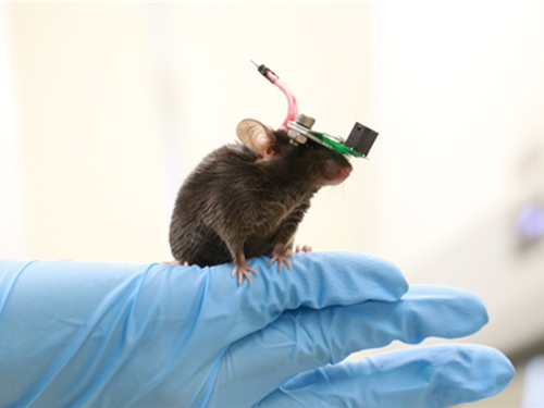 1g-Ultrasound System for the Brain Stimulation of a Freely-moving Mouse
A KAIST research team developed a light-weight capacitive micromachined ultrasonic transducer (CMUT) and succeeded in the ultrasound brain stimulation of a freely-moving mouse. With this lightweight and compact system, researchers can conduct a versatile set of in vivo experiments.
Conventional methods for stimulating a specific brain region, such as deep brain stimulation (DBS) and optogenetics technology, are highly invasive because they have to insert probes into a target brain, which makes them difficult to use for clinical application. While transcranial magnetic stimulation (TMS) and transcranial electrical stimulation (TES) are noninvasive, they have a wide range of stimulation and problems with in-depth stimulation, which makes them problematic for target-specific treatment.
Therefore, noninvasive and focused ultrasound stimulation technology is gaining a great deal of attention as a next-generation brain stimulation alternative. Since it is delivered noninvasively, it can be applied safely in humans as well as animal experiments. Focused ultrasound stimulation is more advantageous than conventional methods in terms of providing both local and deep stimulation.
Animal behavior experiments are essential for brain stimulation research; however, ultrasonic brain stimulation technology is currently in the early stages of development. So far, only research outcomes with fixed anesthetized mice have been studied because of the heavy ultrasonic device.
Professor Hyunjoo J. Lee from the School of Electrical Engineering and her team reported a technology that can provide ultrasound stimulation to the brain of a freely-moving mouse through a microminiaturized ultrasound device.
The team studied miniaturization and ultra-lightweight CMUTs through microelectromechanical systems (MEMS) technology and designed a device suitable for behavior experiments. The device weighing less than 1g (around 0.05% of the mouse’s weight) has the center frequency, size, focal length, and ultrasonic intensity to fit a mouse’s dimensions.
To evaluate the performance of the ultrasonic device, the team stimulated the motor cortex of the mouse brain and observed the movement reaction of its forefoot. They also measured the electromyography (EMG) of the trapezius.
As a result, the team confirmed that their ultrasonic device can deliver ultrasound to a depth of 3-4mm in the mouse brain and stimulate an area of the mouse brain that represents 25% of its total size.
Based on this research, the team is investigating the effects of ultrasound on sleep by stimulating the brain of sleeping mice.
Professor Lee said, “Going beyond experimenting on fixed anesthetized mice, this research succeeded in the brain stimulation of a freely-moving mouse. We are planning to study mice with diseases, such as Parkinson’s disease, dementia, depression, and epilepsy. I believe that this basic research can contribute to treating human brain-related diseases through ultrasound brain stimulation.
This research, led by Masters candidates Hyunggug Kim and Seongyeon Kim, was published in Brain Stimulation (10.1016/j.brs.2018.11.007) on November 17, 2018.
Figure 1. The miniature transducer for the transcranial ultrasound of a freely-moving mouse
Figure 2. Its structure and simulated 2D beam profile in the axial ad radial directions
2019.03.13 View 10389
1g-Ultrasound System for the Brain Stimulation of a Freely-moving Mouse
A KAIST research team developed a light-weight capacitive micromachined ultrasonic transducer (CMUT) and succeeded in the ultrasound brain stimulation of a freely-moving mouse. With this lightweight and compact system, researchers can conduct a versatile set of in vivo experiments.
Conventional methods for stimulating a specific brain region, such as deep brain stimulation (DBS) and optogenetics technology, are highly invasive because they have to insert probes into a target brain, which makes them difficult to use for clinical application. While transcranial magnetic stimulation (TMS) and transcranial electrical stimulation (TES) are noninvasive, they have a wide range of stimulation and problems with in-depth stimulation, which makes them problematic for target-specific treatment.
Therefore, noninvasive and focused ultrasound stimulation technology is gaining a great deal of attention as a next-generation brain stimulation alternative. Since it is delivered noninvasively, it can be applied safely in humans as well as animal experiments. Focused ultrasound stimulation is more advantageous than conventional methods in terms of providing both local and deep stimulation.
Animal behavior experiments are essential for brain stimulation research; however, ultrasonic brain stimulation technology is currently in the early stages of development. So far, only research outcomes with fixed anesthetized mice have been studied because of the heavy ultrasonic device.
Professor Hyunjoo J. Lee from the School of Electrical Engineering and her team reported a technology that can provide ultrasound stimulation to the brain of a freely-moving mouse through a microminiaturized ultrasound device.
The team studied miniaturization and ultra-lightweight CMUTs through microelectromechanical systems (MEMS) technology and designed a device suitable for behavior experiments. The device weighing less than 1g (around 0.05% of the mouse’s weight) has the center frequency, size, focal length, and ultrasonic intensity to fit a mouse’s dimensions.
To evaluate the performance of the ultrasonic device, the team stimulated the motor cortex of the mouse brain and observed the movement reaction of its forefoot. They also measured the electromyography (EMG) of the trapezius.
As a result, the team confirmed that their ultrasonic device can deliver ultrasound to a depth of 3-4mm in the mouse brain and stimulate an area of the mouse brain that represents 25% of its total size.
Based on this research, the team is investigating the effects of ultrasound on sleep by stimulating the brain of sleeping mice.
Professor Lee said, “Going beyond experimenting on fixed anesthetized mice, this research succeeded in the brain stimulation of a freely-moving mouse. We are planning to study mice with diseases, such as Parkinson’s disease, dementia, depression, and epilepsy. I believe that this basic research can contribute to treating human brain-related diseases through ultrasound brain stimulation.
This research, led by Masters candidates Hyunggug Kim and Seongyeon Kim, was published in Brain Stimulation (10.1016/j.brs.2018.11.007) on November 17, 2018.
Figure 1. The miniature transducer for the transcranial ultrasound of a freely-moving mouse
Figure 2. Its structure and simulated 2D beam profile in the axial ad radial directions
2019.03.13 View 10389 -
 KAIST Develops Analog Memristive Synapses for Neuromorphic Chips
(Professor Sung-Yool Choi from the School of Electrical Engineering)
A KAIST research team developed a technology that makes a transition of the operation mode of flexible memristors to synaptic analog switching by reducing the size of the formed filament. Through this technology, memristors can extend their role to memristive synapses for neuromorphic chips, which will lead to developing soft neuromorphic intelligent systems.
Brain-inspired neuromorphic chips have been gaining a great deal of attention for reducing the power consumption and integrating data processing, compared to conventional semiconductor chips. Similarly, memristors are known to be the most suitable candidate for making a crossbar array which is the most efficient architecture for realizing hardware-based artificial neural network (ANN) inside a neuromorphic chip.
A hardware-based ANN consists of a neuron circuit and synapse elements, the connecting pieces. In the neuromorphic system, the synaptic weight, which represents the connection strength between neurons, should be stored and updated as the type of analog data at each synapse.
However, most memristors have digital characteristics suitable for nonvolatile memory. These characteristics put a limitation on the analog operation of the memristors, which makes it difficult to apply them to synaptic devices.
Professor Sung-Yool Choi from the School of Electrical Engineering and his team fabricated a flexible polymer memristor on a plastic substrate, and found that changing the size of the conductive metal filaments formed inside the device on the scale of metal atoms can make a transition of the memristor behavior from digital to analog.
Using this phenomenon, the team developed flexible memristor-based electronic synapses, which can continuously and linearly update synaptic weight, and operate under mechanical deformations such as bending.
The team confirmed that the ANN based on these memristor synapses can effectively classify person’s facial images even when they were damaged. This research demonstrated the possibility of a neuromorphic chip that can efficiently recognize faces, numbers, and objects.
Professor Choi said, “We found the principles underlying the transition from digital to analog operation of the memristors. I believe that this research paves the way for applying various memristors to either digital memory or electronic synapses, and will accelerate the development of a high-performing neuromorphic chip.”
In a joint research project with Professor Sung Gap Im (KAIST) and Professor V. P. Dravid (Northwestern University), this study was led by Dr. Byung Chul Jang (Samsung Electronics), Dr. Sungkyu Kim (Northwestern University) and Dr. Sang Yoon Yang (KAIST), and was published online in Nano Letters (10.1021/acs.nanolett.8b04023) on January 4, 2019.
Figure 1. a) Schematic illustration of a flexible pV3D3 memristor-based electronic synapse array. b) Cross-sectional TEM image of the flexible pV3D3 memristor
2019.02.28 View 11330
KAIST Develops Analog Memristive Synapses for Neuromorphic Chips
(Professor Sung-Yool Choi from the School of Electrical Engineering)
A KAIST research team developed a technology that makes a transition of the operation mode of flexible memristors to synaptic analog switching by reducing the size of the formed filament. Through this technology, memristors can extend their role to memristive synapses for neuromorphic chips, which will lead to developing soft neuromorphic intelligent systems.
Brain-inspired neuromorphic chips have been gaining a great deal of attention for reducing the power consumption and integrating data processing, compared to conventional semiconductor chips. Similarly, memristors are known to be the most suitable candidate for making a crossbar array which is the most efficient architecture for realizing hardware-based artificial neural network (ANN) inside a neuromorphic chip.
A hardware-based ANN consists of a neuron circuit and synapse elements, the connecting pieces. In the neuromorphic system, the synaptic weight, which represents the connection strength between neurons, should be stored and updated as the type of analog data at each synapse.
However, most memristors have digital characteristics suitable for nonvolatile memory. These characteristics put a limitation on the analog operation of the memristors, which makes it difficult to apply them to synaptic devices.
Professor Sung-Yool Choi from the School of Electrical Engineering and his team fabricated a flexible polymer memristor on a plastic substrate, and found that changing the size of the conductive metal filaments formed inside the device on the scale of metal atoms can make a transition of the memristor behavior from digital to analog.
Using this phenomenon, the team developed flexible memristor-based electronic synapses, which can continuously and linearly update synaptic weight, and operate under mechanical deformations such as bending.
The team confirmed that the ANN based on these memristor synapses can effectively classify person’s facial images even when they were damaged. This research demonstrated the possibility of a neuromorphic chip that can efficiently recognize faces, numbers, and objects.
Professor Choi said, “We found the principles underlying the transition from digital to analog operation of the memristors. I believe that this research paves the way for applying various memristors to either digital memory or electronic synapses, and will accelerate the development of a high-performing neuromorphic chip.”
In a joint research project with Professor Sung Gap Im (KAIST) and Professor V. P. Dravid (Northwestern University), this study was led by Dr. Byung Chul Jang (Samsung Electronics), Dr. Sungkyu Kim (Northwestern University) and Dr. Sang Yoon Yang (KAIST), and was published online in Nano Letters (10.1021/acs.nanolett.8b04023) on January 4, 2019.
Figure 1. a) Schematic illustration of a flexible pV3D3 memristor-based electronic synapse array. b) Cross-sectional TEM image of the flexible pV3D3 memristor
2019.02.28 View 11330 -
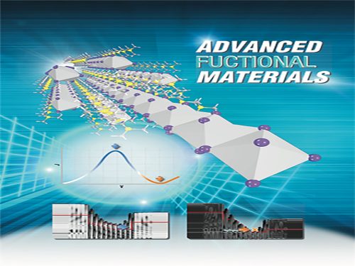 Novel Material Properties of Hybrid Perovskite Nanostructures for Next-generation Non-linear Electronic Devices
(from left: Juho Lee, Dr. Muhammad Ejaz Khan and Professor Yong-Hoon Kim)
A KAIST research team reported a novel non-linear device with the founding property coming from perovskite nanowires. They showed that hybrid perovskite-derived, inorganic-framework nanowires can acquire semi-metallicity, and proposed negative differential resistance (NDR) devices with excellent NDR characteristics that resulted from a novel quantum-hybridization NDR mechanism, implying the potential of perovskite nanowires to be realized in next-generation electronic devices.
Organic-inorganic hybrid halide perovskites have recently emerged as prominent candidates for photonic applications due to their excellent optoelectronic properties as well as their low cost and facile synthesis processes. Prominent progresses have been already made for devices including solar cells, light-emitting diodes, lasers and photodetectors.
However, research on electronic devices based on hybrid halide perovskites has not been actively pursued compared with their photonic device counterparts.
Professor Yong-Hoon Kim from the School of Electrical Engineering and his team took a closer look at low-dimensional organic-inorganic halide perovskite materials, which have enhanced quantum confinement effects, and particularly focused on the recently synthesized trimethylsulfonium (TMS) lead triiodide (CH3)3SPbI3.
Using supercomputer simulations, the team first showed that stripping the (CH3)3S or TMS organic ligands from the TMS PbI3 perovskite nanowires results in semi-metallic PbI3 columns, which contradicts the conventional assumption of the semiconducting or insulating characteristics of the inorganic perovskite framework.
Utilizing the semi-metallic PbI3 inorganic framework as the electrode, the team designed a tunneling junction device from perovskite nanowires and found that they exhibit excellent nonlinear negative differential resistance (NDR) behavior. The NDR property is a key to realizing next-generation, ultra-low-power, and multivalued non-linear devices. Furthermore, the team found that this NDR originates from a novel mechanism that involves the quantum-mechanical hybridization between channel and electrode states.
Professor Kim said, “This research demonstrates the potential of quantum mechanics-based computer simulations to lead developments in advanced nanomaterials and nanodevices. In particular, this research proposes a new direction in the development of a quantum mechanical tunneling device, which was the topic for which the Nobel Laureate in Physics in 1973 was awarded to Dr. Leo Esaki.
This research, led by Dr. Muhammad Ejaz Khan and PhD candidate Juho Lee, was published online in Advanced Functional Materials (10.1002/adfm.201807620) on January 7, 2019.
Figure. The draft version of the cover page of 'Advanced Functional Materials'
2019.02.22 View 8146
Novel Material Properties of Hybrid Perovskite Nanostructures for Next-generation Non-linear Electronic Devices
(from left: Juho Lee, Dr. Muhammad Ejaz Khan and Professor Yong-Hoon Kim)
A KAIST research team reported a novel non-linear device with the founding property coming from perovskite nanowires. They showed that hybrid perovskite-derived, inorganic-framework nanowires can acquire semi-metallicity, and proposed negative differential resistance (NDR) devices with excellent NDR characteristics that resulted from a novel quantum-hybridization NDR mechanism, implying the potential of perovskite nanowires to be realized in next-generation electronic devices.
Organic-inorganic hybrid halide perovskites have recently emerged as prominent candidates for photonic applications due to their excellent optoelectronic properties as well as their low cost and facile synthesis processes. Prominent progresses have been already made for devices including solar cells, light-emitting diodes, lasers and photodetectors.
However, research on electronic devices based on hybrid halide perovskites has not been actively pursued compared with their photonic device counterparts.
Professor Yong-Hoon Kim from the School of Electrical Engineering and his team took a closer look at low-dimensional organic-inorganic halide perovskite materials, which have enhanced quantum confinement effects, and particularly focused on the recently synthesized trimethylsulfonium (TMS) lead triiodide (CH3)3SPbI3.
Using supercomputer simulations, the team first showed that stripping the (CH3)3S or TMS organic ligands from the TMS PbI3 perovskite nanowires results in semi-metallic PbI3 columns, which contradicts the conventional assumption of the semiconducting or insulating characteristics of the inorganic perovskite framework.
Utilizing the semi-metallic PbI3 inorganic framework as the electrode, the team designed a tunneling junction device from perovskite nanowires and found that they exhibit excellent nonlinear negative differential resistance (NDR) behavior. The NDR property is a key to realizing next-generation, ultra-low-power, and multivalued non-linear devices. Furthermore, the team found that this NDR originates from a novel mechanism that involves the quantum-mechanical hybridization between channel and electrode states.
Professor Kim said, “This research demonstrates the potential of quantum mechanics-based computer simulations to lead developments in advanced nanomaterials and nanodevices. In particular, this research proposes a new direction in the development of a quantum mechanical tunneling device, which was the topic for which the Nobel Laureate in Physics in 1973 was awarded to Dr. Leo Esaki.
This research, led by Dr. Muhammad Ejaz Khan and PhD candidate Juho Lee, was published online in Advanced Functional Materials (10.1002/adfm.201807620) on January 7, 2019.
Figure. The draft version of the cover page of 'Advanced Functional Materials'
2019.02.22 View 8146 -
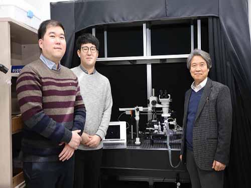 KAIST Develops Core Technology for Ultra-small 3D Image Sensor
(from left: Dr. Jong-Bum Yo, PhD candidate Seong-Hwan Kimand Professor Hyo-Hoon Park)
A KAIST research team developed a silicon optical phased array (OPA) chip, which can be a core component for three-dimensional image sensors. This research was co-led by PhD candidate Seong-Hwan Kim and Dr. Jong-Bum You from the National Nanofab Center (NNFC).
A 3D image sensor adds distance information to a two-dimensional image, such as a photo, to recognize it as a 3D image. It plays a vital role in various electronics including autonomous vehicles, drones, robots, and facial recognition systems, which require accurate measurement of the distance from objects.
Many automobile and drone companies are focusing on developing 3D image sensor systems, based on mechanical light detection and ranging (LiDAR) systems. However, it can only get as small as the size of a fist and has a high possibility of malfunctioning because it employs a mechanical method for laser beam-steering.
OPAs have gained a great attention as a key component to implement solid-state LiDAR because it can control the light direction electronically without moving parts. Silicon-based OPAs are small, durable, and can be mass-produced through conventional Si-CMOS processes.
However, in the development of OPAs, a big issue has been raised about how to achieve wide beam-steering in transversal and longitudinal directions. In the transversal direction, a wide beam-steering has been implemented, relatively easily, through a thermo-optic or electro-optic control of the phase shifters integrated with a 1D array. But the longitudinal beam-steering has been remaining as a technical challenge since only a narrow steering was possible with the same 1D array by changing the wavelengths of light, which is hard to implement in semiconductor processes.
If a light wavelength is changed, characteristics of element devices consisting the OPA can vary, which makes it difficult to control the light direction with reliability as well as to integrate a wavelength-tunable laser on a silicon-based chip. Therefore, it is essential to devise a new structure that can easily adjust the radiated light in both transversal and longitudinal directions.
By integrating tunable radiator, instead of tunable laser in a conventional OPA, Professor Hyo-Hoon Park from the School of Electrical Engineering and his team developed an ultra-small, low-power OPA chip that facilitates a wide 2D beam-steering with a monochromatic light source.
This OPA structure allows the minimizing of the 3D image sensors, as small as a dragonfly’s eye.
According to the team, the OPA can function as a 3D image sensor and also as a wireless transmitter sending the image data to a desired direction, enabling high-quality image data to be freely communicated between electronic devices.
Kim said, “It’s not an easy task to integrate a tunable light source in the OPA structures of previous works. We hope our research proposing a tunable radiator makes a big step towards commercializing OPAs.”
Dr. You added, “We will be able to support application researches of 3D image sensors, especially for facial recognition with smartphones and augmented reality services. We will try to prepare a processing platform in NNFC that provides core technologies of the 3D image sensor fabrication.”
This research was published in Optics Letters on January 15.
Figure 1.The manufactured OPA chip
Figure 2. Schematic feature showing an application of the OPA to a 3D image sensor
2019.02.08 View 8165
KAIST Develops Core Technology for Ultra-small 3D Image Sensor
(from left: Dr. Jong-Bum Yo, PhD candidate Seong-Hwan Kimand Professor Hyo-Hoon Park)
A KAIST research team developed a silicon optical phased array (OPA) chip, which can be a core component for three-dimensional image sensors. This research was co-led by PhD candidate Seong-Hwan Kim and Dr. Jong-Bum You from the National Nanofab Center (NNFC).
A 3D image sensor adds distance information to a two-dimensional image, such as a photo, to recognize it as a 3D image. It plays a vital role in various electronics including autonomous vehicles, drones, robots, and facial recognition systems, which require accurate measurement of the distance from objects.
Many automobile and drone companies are focusing on developing 3D image sensor systems, based on mechanical light detection and ranging (LiDAR) systems. However, it can only get as small as the size of a fist and has a high possibility of malfunctioning because it employs a mechanical method for laser beam-steering.
OPAs have gained a great attention as a key component to implement solid-state LiDAR because it can control the light direction electronically without moving parts. Silicon-based OPAs are small, durable, and can be mass-produced through conventional Si-CMOS processes.
However, in the development of OPAs, a big issue has been raised about how to achieve wide beam-steering in transversal and longitudinal directions. In the transversal direction, a wide beam-steering has been implemented, relatively easily, through a thermo-optic or electro-optic control of the phase shifters integrated with a 1D array. But the longitudinal beam-steering has been remaining as a technical challenge since only a narrow steering was possible with the same 1D array by changing the wavelengths of light, which is hard to implement in semiconductor processes.
If a light wavelength is changed, characteristics of element devices consisting the OPA can vary, which makes it difficult to control the light direction with reliability as well as to integrate a wavelength-tunable laser on a silicon-based chip. Therefore, it is essential to devise a new structure that can easily adjust the radiated light in both transversal and longitudinal directions.
By integrating tunable radiator, instead of tunable laser in a conventional OPA, Professor Hyo-Hoon Park from the School of Electrical Engineering and his team developed an ultra-small, low-power OPA chip that facilitates a wide 2D beam-steering with a monochromatic light source.
This OPA structure allows the minimizing of the 3D image sensors, as small as a dragonfly’s eye.
According to the team, the OPA can function as a 3D image sensor and also as a wireless transmitter sending the image data to a desired direction, enabling high-quality image data to be freely communicated between electronic devices.
Kim said, “It’s not an easy task to integrate a tunable light source in the OPA structures of previous works. We hope our research proposing a tunable radiator makes a big step towards commercializing OPAs.”
Dr. You added, “We will be able to support application researches of 3D image sensors, especially for facial recognition with smartphones and augmented reality services. We will try to prepare a processing platform in NNFC that provides core technologies of the 3D image sensor fabrication.”
This research was published in Optics Letters on January 15.
Figure 1.The manufactured OPA chip
Figure 2. Schematic feature showing an application of the OPA to a 3D image sensor
2019.02.08 View 8165 -
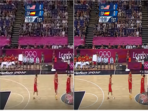 Enhanced Video Quality despite Poor Network Conditions
(from left: Jaehong Kim, Youngmok Jung, Hyunho Yeo, Professor Dongsu Han and Professor Jinwoo Shin)
Professor Jinwoo Shin and Professor Dongsu Han from the School of Electrical Engineering developed neural adaptive content-aware internet video delivery. This technology is a novel method that combines adaptive streaming over HTTP, the video transmission system adopted by YouTube and Netflix, with a deep learning model.
This technology is expected to create an internet environment where users can enjoy watching 4K and AV/VR videos with high-quality and high-definition (HD) videos even with weak internet connections.
Thanks to video streaming services, internet video has experienced remarkable growth; nevertheless, users often suffer from low video quality due to unfavorable network conditions. Currently, existing adaptive streaming systems adjust the quality of the video in real time, accommodating the continuously changing internet bandwidth. Various algorithms are being researched for adaptive streaming systems, but there is an inherent limitation; that is, high-quality videos cannot be streamed in poor network environments regardless of which algorithm is used.
By incorporating super-resolution in adaptive streaming, the team overcame the limit of existing content distribution networks, of which their quality relies too much on the bandwidth. In the conventional method, the server that provides the video splits a video into certain lengths of time in advance. But the novel system introduced by the team allows the downloading of neural network segments. To facilitate this method, the video server needs to provide deep neural networks for each video segment as well as sizes of Deep Neural Networks (DNN) according to the specifications of the user’s computing capacity.
The largest neural network size is two megabytes, which is considerably smaller than video. When downloading the neural network from the user’s video player, it is split into several segments. Even its partial download is sufficient for a slightly comprised super-resolution.
While playing the video, the system converts the low quality video to a high-quality version by employing super-resolution based on deep convolution neural networks (CNN). The entire process is done in real time, and users can enjoy the high-definition video.
Even with a 17% smaller bandwidth, the system can provide the Quality of Experience equivalent to the latest adaptive streaming service. At a given internet bandwidth, it can provide 43% higher average QoE than the latest service.
Using a deep learning method allows this system to achieve a higher level of compression than the existing video compression methods. Their technology was recognized as a next-generation internet video system that applies super-resolution based on a deep convolution neural network to online videos.
Professor Han said, “So far, it has only been implemented on desktops, but we will further develop applications that work in mobile devices as well. This technology has been applied to the same video transmission systems used by streaming channels such as YouTube and Netflix, and thus shows good signs for practicability.”
This research, led by Hyunho Yeo, Youngmok Jung and Jaehong Kim, was presented at the 13th UNSENIX OSDI conference on October 10 2018 and completed for filing international patent application.
For further information, please click here.
Figure 1. Image quality before (left) and after (right) the technology application
Figure 2. The technology Concept
Figure 3. A transition from low-quality to high quality video after video transmission from the video server
2019.01.22 View 7815
Enhanced Video Quality despite Poor Network Conditions
(from left: Jaehong Kim, Youngmok Jung, Hyunho Yeo, Professor Dongsu Han and Professor Jinwoo Shin)
Professor Jinwoo Shin and Professor Dongsu Han from the School of Electrical Engineering developed neural adaptive content-aware internet video delivery. This technology is a novel method that combines adaptive streaming over HTTP, the video transmission system adopted by YouTube and Netflix, with a deep learning model.
This technology is expected to create an internet environment where users can enjoy watching 4K and AV/VR videos with high-quality and high-definition (HD) videos even with weak internet connections.
Thanks to video streaming services, internet video has experienced remarkable growth; nevertheless, users often suffer from low video quality due to unfavorable network conditions. Currently, existing adaptive streaming systems adjust the quality of the video in real time, accommodating the continuously changing internet bandwidth. Various algorithms are being researched for adaptive streaming systems, but there is an inherent limitation; that is, high-quality videos cannot be streamed in poor network environments regardless of which algorithm is used.
By incorporating super-resolution in adaptive streaming, the team overcame the limit of existing content distribution networks, of which their quality relies too much on the bandwidth. In the conventional method, the server that provides the video splits a video into certain lengths of time in advance. But the novel system introduced by the team allows the downloading of neural network segments. To facilitate this method, the video server needs to provide deep neural networks for each video segment as well as sizes of Deep Neural Networks (DNN) according to the specifications of the user’s computing capacity.
The largest neural network size is two megabytes, which is considerably smaller than video. When downloading the neural network from the user’s video player, it is split into several segments. Even its partial download is sufficient for a slightly comprised super-resolution.
While playing the video, the system converts the low quality video to a high-quality version by employing super-resolution based on deep convolution neural networks (CNN). The entire process is done in real time, and users can enjoy the high-definition video.
Even with a 17% smaller bandwidth, the system can provide the Quality of Experience equivalent to the latest adaptive streaming service. At a given internet bandwidth, it can provide 43% higher average QoE than the latest service.
Using a deep learning method allows this system to achieve a higher level of compression than the existing video compression methods. Their technology was recognized as a next-generation internet video system that applies super-resolution based on a deep convolution neural network to online videos.
Professor Han said, “So far, it has only been implemented on desktops, but we will further develop applications that work in mobile devices as well. This technology has been applied to the same video transmission systems used by streaming channels such as YouTube and Netflix, and thus shows good signs for practicability.”
This research, led by Hyunho Yeo, Youngmok Jung and Jaehong Kim, was presented at the 13th UNSENIX OSDI conference on October 10 2018 and completed for filing international patent application.
For further information, please click here.
Figure 1. Image quality before (left) and after (right) the technology application
Figure 2. The technology Concept
Figure 3. A transition from low-quality to high quality video after video transmission from the video server
2019.01.22 View 7815