Global+Singularity+Research+Program
-
 KAIST Turns an Unprecedented Idea into Reality: Quantum Computing with Magnets
What started as an idea under KAIST’s Global Singularity Research Project—"Can we build a quantum computer using magnets?"—has now become a scientific reality. A KAIST-led international research team has successfully demonstrated a core quantum computing technology using magnetic materials (ferromagnets) for the first time in the world.
KAIST (represented by President Kwang-Hyung Lee) announced on the 6th of May that a team led by Professor Kab-Jin Kim from the Department of Physics, in collaboration with the Argonne National Laboratory and the University of Illinois Urbana-Champaign (UIUC), has developed a “photon-magnon hybrid chip” and successfully implemented real-time, multi-pulse interference using magnetic materials—marking a global first.
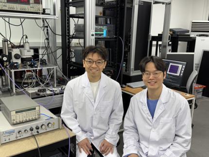
< Photo 1. Dr. Moojune Song (left) and Professor Kab-Jin Kim (right) of KAIST Department of Physics >
In simple terms, the researchers developed a special chip that synchronizes light and internal magnetic vibrations (magnons), enabling the transmission of phase information between distant magnets. They succeeded in observing and controlling interference between multiple signals in real time. This marks the first experimental evidence that magnets can serve as key components in quantum computing, serving as a pivotal step toward magnet-based quantum platforms.
The N and S poles of a magnet stem from the spin of electrons inside atoms. When many atoms align, their collective spin vibrations create a quantum particle known as a “magnon.”
Magnons are especially promising because of their nonreciprocal nature—they can carry information in only one direction, which makes them suitable for quantum noise isolation in compact quantum chips. They can also couple with both light and microwaves, enabling the potential for long-distance quantum communication over tens of kilometers.
Moreover, using special materials like antiferromagnets could allow quantum computers to operate at terahertz (THz) frequencies, far surpassing today’s hardware limitations, and possibly enabling room-temperature quantum computing without the need for bulky cryogenic equipment.
To build such a system, however, one must be able to transmit, measure, and control the phase information of magnons—the starting point and propagation of their waveforms—in real time. This had not been achieved until now.
< Figure 1. Superconducting Circuit-Based Magnon-Photon Hybrid System. (a) Schematic diagram of the device. A NbN superconducting resonator circuit fabricated on a silicon substrate is coupled with spherical YIG magnets (250 μm diameter), and magnons are generated and measured in real-time via a vertical antenna. (b) Photograph of the actual device. The distance between the two YIG spheres is 12 mm, a distance at which they cannot influence each other without the superconducting circuit. >
Professor Kim’s team used two tiny magnetic spheres made of Yttrium Iron Garnet (YIG) placed 12 mm apart with a superconducting resonator in between—similar to those used in quantum processors by Google and IBM. They input pulses into one magnet and successfully observed lossless transmission of magnon vibrations to the second magnet via the superconducting circuit.
They confirmed that from single nanosecond pulses to four microwave pulses, the magnon vibrations maintained their phase information and demonstrated predictable constructive or destructive interference in real time—known as coherent interference.
By adjusting the pulse frequencies and their intervals, the researchers could also freely control the interference patterns of magnons, effectively showing for the first time that electrical signals can be used to manipulate magnonic quantum states.
This work demonstrated that quantum gate operations using multiple pulses—a fundamental technique in quantum information processing—can be implemented using a hybrid system of magnetic materials and superconducting circuits. This opens the door for the practical use of magnet-based quantum devices.
< Figure 2. Experimental Data. (a) Measurement results of magnon-magnon band anticrossing via continuous wave measurement, showing the formation of a strong coupling hybrid system. (b) Magnon pulse exchange oscillation phenomenon between YIG spheres upon single pulse application. It can be seen that magnon information is coherently transmitted at regular time intervals through the superconducting circuit. (c,d) Magnon interference phenomenon upon dual pulse application. The magnon information state can be arbitrarily controlled by adjusting the time interval and carrier frequency between pulses. >
Professor Kab-Jin Kim stated, “This project began with a bold, even unconventional idea proposed to the Global Singularity Research Program: ‘What if we could build a quantum computer with magnets?’ The journey has been fascinating, and this study not only opens a new field of quantum spintronics, but also marks a turning point in developing high-efficiency quantum information processing devices.”
The research was co-led by postdoctoral researcher Moojune Song (KAIST), Dr. Yi Li and Dr. Valentine Novosad from Argonne National Lab, and Prof. Axel Hoffmann’s team at UIUC. The results were published in Nature Communications on April 17 and npj Spintronics on April 1, 2025.
Paper 1: Single-shot magnon interference in a magnon-superconducting-resonator hybrid circuit, Nat. Commun. 16, 3649 (2025)
DOI: https://doi.org/10.1038/s41467-025-58482-2
Paper 2: Single-shot electrical detection of short-wavelength magnon pulse transmission in a magnonic ultra-thin-film waveguide, npj Spintronics 3, 12 (2025)
DOI: https://doi.org/10.1038/s44306-025-00072-5
The research was supported by KAIST’s Global Singularity Research Initiative, the National Research Foundation of Korea (including the Mid-Career Researcher, Leading Research Center, and Quantum Information Science Human Resource Development programs), and the U.S. Department of Energy.
2025.06.12 View 345
KAIST Turns an Unprecedented Idea into Reality: Quantum Computing with Magnets
What started as an idea under KAIST’s Global Singularity Research Project—"Can we build a quantum computer using magnets?"—has now become a scientific reality. A KAIST-led international research team has successfully demonstrated a core quantum computing technology using magnetic materials (ferromagnets) for the first time in the world.
KAIST (represented by President Kwang-Hyung Lee) announced on the 6th of May that a team led by Professor Kab-Jin Kim from the Department of Physics, in collaboration with the Argonne National Laboratory and the University of Illinois Urbana-Champaign (UIUC), has developed a “photon-magnon hybrid chip” and successfully implemented real-time, multi-pulse interference using magnetic materials—marking a global first.
< Photo 1. Dr. Moojune Song (left) and Professor Kab-Jin Kim (right) of KAIST Department of Physics >
In simple terms, the researchers developed a special chip that synchronizes light and internal magnetic vibrations (magnons), enabling the transmission of phase information between distant magnets. They succeeded in observing and controlling interference between multiple signals in real time. This marks the first experimental evidence that magnets can serve as key components in quantum computing, serving as a pivotal step toward magnet-based quantum platforms.
The N and S poles of a magnet stem from the spin of electrons inside atoms. When many atoms align, their collective spin vibrations create a quantum particle known as a “magnon.”
Magnons are especially promising because of their nonreciprocal nature—they can carry information in only one direction, which makes them suitable for quantum noise isolation in compact quantum chips. They can also couple with both light and microwaves, enabling the potential for long-distance quantum communication over tens of kilometers.
Moreover, using special materials like antiferromagnets could allow quantum computers to operate at terahertz (THz) frequencies, far surpassing today’s hardware limitations, and possibly enabling room-temperature quantum computing without the need for bulky cryogenic equipment.
To build such a system, however, one must be able to transmit, measure, and control the phase information of magnons—the starting point and propagation of their waveforms—in real time. This had not been achieved until now.
< Figure 1. Superconducting Circuit-Based Magnon-Photon Hybrid System. (a) Schematic diagram of the device. A NbN superconducting resonator circuit fabricated on a silicon substrate is coupled with spherical YIG magnets (250 μm diameter), and magnons are generated and measured in real-time via a vertical antenna. (b) Photograph of the actual device. The distance between the two YIG spheres is 12 mm, a distance at which they cannot influence each other without the superconducting circuit. >
Professor Kim’s team used two tiny magnetic spheres made of Yttrium Iron Garnet (YIG) placed 12 mm apart with a superconducting resonator in between—similar to those used in quantum processors by Google and IBM. They input pulses into one magnet and successfully observed lossless transmission of magnon vibrations to the second magnet via the superconducting circuit.
They confirmed that from single nanosecond pulses to four microwave pulses, the magnon vibrations maintained their phase information and demonstrated predictable constructive or destructive interference in real time—known as coherent interference.
By adjusting the pulse frequencies and their intervals, the researchers could also freely control the interference patterns of magnons, effectively showing for the first time that electrical signals can be used to manipulate magnonic quantum states.
This work demonstrated that quantum gate operations using multiple pulses—a fundamental technique in quantum information processing—can be implemented using a hybrid system of magnetic materials and superconducting circuits. This opens the door for the practical use of magnet-based quantum devices.
< Figure 2. Experimental Data. (a) Measurement results of magnon-magnon band anticrossing via continuous wave measurement, showing the formation of a strong coupling hybrid system. (b) Magnon pulse exchange oscillation phenomenon between YIG spheres upon single pulse application. It can be seen that magnon information is coherently transmitted at regular time intervals through the superconducting circuit. (c,d) Magnon interference phenomenon upon dual pulse application. The magnon information state can be arbitrarily controlled by adjusting the time interval and carrier frequency between pulses. >
Professor Kab-Jin Kim stated, “This project began with a bold, even unconventional idea proposed to the Global Singularity Research Program: ‘What if we could build a quantum computer with magnets?’ The journey has been fascinating, and this study not only opens a new field of quantum spintronics, but also marks a turning point in developing high-efficiency quantum information processing devices.”
The research was co-led by postdoctoral researcher Moojune Song (KAIST), Dr. Yi Li and Dr. Valentine Novosad from Argonne National Lab, and Prof. Axel Hoffmann’s team at UIUC. The results were published in Nature Communications on April 17 and npj Spintronics on April 1, 2025.
Paper 1: Single-shot magnon interference in a magnon-superconducting-resonator hybrid circuit, Nat. Commun. 16, 3649 (2025)
DOI: https://doi.org/10.1038/s41467-025-58482-2
Paper 2: Single-shot electrical detection of short-wavelength magnon pulse transmission in a magnonic ultra-thin-film waveguide, npj Spintronics 3, 12 (2025)
DOI: https://doi.org/10.1038/s44306-025-00072-5
The research was supported by KAIST’s Global Singularity Research Initiative, the National Research Foundation of Korea (including the Mid-Career Researcher, Leading Research Center, and Quantum Information Science Human Resource Development programs), and the U.S. Department of Energy.
2025.06.12 View 345 -
 Streamlining the Process of Materials Discovery
The materials platform M3I3 reduces the time for materials discovery by reverse engineering future materials using multiscale/multimodal imaging and machine learning of the processing-structure-properties relationship
Developing new materials and novel processes has continued to change the world. The M3I3 Initiative at KAIST has led to new insights into advancing materials development by implementing breakthroughs in materials imaging that have created a paradigm shift in the discovery of materials. The Initiative features the multiscale modeling and imaging of structure and property relationships and materials hierarchies combined with the latest material-processing data.
The research team led by Professor Seungbum Hong analyzed the materials research projects reported by leading global institutes and research groups, and derived a quantitative model using machine learning with a scientific interpretation. This process embodies the research goal of the M3I3: Materials and Molecular Modeling, Imaging, Informatics and Integration.
The researchers discussed the role of multiscale materials and molecular imaging combined with machine learning and also presented a future outlook for developments and the major challenges of M3I3. By building this model, the research team envisions creating desired sets of properties for materials and obtaining the optimum processing recipes to synthesize them.
“The development of various microscopy and diffraction tools with the ability to map the structure, property, and performance of materials at multiscale levels and in real time enabled us to think that materials imaging could radically accelerate materials discovery and development,” says Professor Hong.
“We plan to build an M3I3 repository of searchable structural and property maps using FAIR (Findable, Accessible, Interoperable, and Reusable) principles to standardize best practices as well as streamline the training of early career researchers.”
One of the examples that shows the power of structure-property imaging at the nanoscale is the development of future materials for emerging nonvolatile memory devices. Specifically, the research team focused on microscopy using photons, electrons, and physical probes on the multiscale structural hierarchy, as well as structure-property relationships to enhance the performance of memory devices.
“M3I3 is an algorithm for performing the reverse engineering of future materials. Reverse engineering starts by analyzing the structure and composition of cutting-edge materials or products. Once the research team determines the performance of our targeted future materials, we need to know the candidate structures and compositions for producing the future materials.”
The research team has built a data-driven experimental design based on traditional NCM (nickel, cobalt, and manganese) cathode materials. With this, the research team expanded their future direction for achieving even higher discharge capacity, which can be realized via Li-rich cathodes.
However, one of the major challenges was the limitation of available data that describes the Li-rich cathode properties. To mitigate this problem, the researchers proposed two solutions: First, they should build a machine-learning-guided data generator for data augmentation. Second, they would use a machine-learning method based on ‘transfer learning.’ Since the NCM cathode database shares a common feature with a Li-rich cathode, one could consider repurposing the NCM trained model for assisting the Li-rich prediction. With the pretrained model and transfer learning, the team expects to achieve outstanding predictions for Li-rich cathodes even with the small data set.
With advances in experimental imaging and the availability of well-resolved information and big data, along with significant advances in high-performance computing and a worldwide thrust toward a general, collaborative, integrative, and on-demand research platform, there is a clear confluence in the required capabilities of advancing the M3I3 Initiative.
Professor Hong said, “Once we succeed in using the inverse “property−structure−processing” solver to develop cathode, anode, electrolyte, and membrane materials for high energy density Li-ion batteries, we will expand our scope of materials to battery/fuel cells, aerospace, automobiles, food, medicine, and cosmetic materials.”
The review was published in ACS Nano in March. This study was conducted through collaborations with Dr. Chi Hao Liow, Professor Jong Min Yuk, Professor Hye Ryung Byon, Professor Yongsoo Yang, Professor EunAe Cho, Professor Pyuck-Pa Choi, and Professor Hyuck Mo Lee at KAIST, Professor Joshua C. Agar at Lehigh University, Dr. Sergei V. Kalinin at Oak Ridge National Laboratory, Professor Peter W. Voorhees at Northwestern University, and Professor Peter Littlewood at the University of Chicago (Article title: Reducing Time to Discovery: Materials and Molecular Modeling, Imaging, Informatics, and Integration).This work was supported by the KAIST Global Singularity Research Program for 2019 and 2020.
Publication:
“Reducing Time to Discovery: Materials and Molecular Modeling, Imaging, Informatics and Integration,” S. Hong, C. H. Liow, J. M. Yuk, H. R. Byon, Y. Yang, E. Cho, J. Yeom, G. Park, H. Kang, S. Kim, Y. Shim, M. Na, C. Jeong, G. Hwang, H. Kim, H. Kim, S. Eom, S. Cho, H. Jun, Y. Lee, A. Baucour, K. Bang, M. Kim, S. Yun, J. Ryu, Y. Han, A. Jetybayeva, P.-P. Choi, J. C. Agar, S. V. Kalinin, P. W. Voorhees, P. Littlewood, and H. M. Lee, ACS Nano 15, 3, 3971–3995 (2021) https://doi.org/10.1021/acsnano.1c00211
Profile:
Seungbum Hong, PhD
Associate Professor
seungbum@kaist.ac.kr
http://mii.kaist.ac.kr
Department of Materials Science and Engineering
KAIST
(END)
2021.04.05 View 14468
Streamlining the Process of Materials Discovery
The materials platform M3I3 reduces the time for materials discovery by reverse engineering future materials using multiscale/multimodal imaging and machine learning of the processing-structure-properties relationship
Developing new materials and novel processes has continued to change the world. The M3I3 Initiative at KAIST has led to new insights into advancing materials development by implementing breakthroughs in materials imaging that have created a paradigm shift in the discovery of materials. The Initiative features the multiscale modeling and imaging of structure and property relationships and materials hierarchies combined with the latest material-processing data.
The research team led by Professor Seungbum Hong analyzed the materials research projects reported by leading global institutes and research groups, and derived a quantitative model using machine learning with a scientific interpretation. This process embodies the research goal of the M3I3: Materials and Molecular Modeling, Imaging, Informatics and Integration.
The researchers discussed the role of multiscale materials and molecular imaging combined with machine learning and also presented a future outlook for developments and the major challenges of M3I3. By building this model, the research team envisions creating desired sets of properties for materials and obtaining the optimum processing recipes to synthesize them.
“The development of various microscopy and diffraction tools with the ability to map the structure, property, and performance of materials at multiscale levels and in real time enabled us to think that materials imaging could radically accelerate materials discovery and development,” says Professor Hong.
“We plan to build an M3I3 repository of searchable structural and property maps using FAIR (Findable, Accessible, Interoperable, and Reusable) principles to standardize best practices as well as streamline the training of early career researchers.”
One of the examples that shows the power of structure-property imaging at the nanoscale is the development of future materials for emerging nonvolatile memory devices. Specifically, the research team focused on microscopy using photons, electrons, and physical probes on the multiscale structural hierarchy, as well as structure-property relationships to enhance the performance of memory devices.
“M3I3 is an algorithm for performing the reverse engineering of future materials. Reverse engineering starts by analyzing the structure and composition of cutting-edge materials or products. Once the research team determines the performance of our targeted future materials, we need to know the candidate structures and compositions for producing the future materials.”
The research team has built a data-driven experimental design based on traditional NCM (nickel, cobalt, and manganese) cathode materials. With this, the research team expanded their future direction for achieving even higher discharge capacity, which can be realized via Li-rich cathodes.
However, one of the major challenges was the limitation of available data that describes the Li-rich cathode properties. To mitigate this problem, the researchers proposed two solutions: First, they should build a machine-learning-guided data generator for data augmentation. Second, they would use a machine-learning method based on ‘transfer learning.’ Since the NCM cathode database shares a common feature with a Li-rich cathode, one could consider repurposing the NCM trained model for assisting the Li-rich prediction. With the pretrained model and transfer learning, the team expects to achieve outstanding predictions for Li-rich cathodes even with the small data set.
With advances in experimental imaging and the availability of well-resolved information and big data, along with significant advances in high-performance computing and a worldwide thrust toward a general, collaborative, integrative, and on-demand research platform, there is a clear confluence in the required capabilities of advancing the M3I3 Initiative.
Professor Hong said, “Once we succeed in using the inverse “property−structure−processing” solver to develop cathode, anode, electrolyte, and membrane materials for high energy density Li-ion batteries, we will expand our scope of materials to battery/fuel cells, aerospace, automobiles, food, medicine, and cosmetic materials.”
The review was published in ACS Nano in March. This study was conducted through collaborations with Dr. Chi Hao Liow, Professor Jong Min Yuk, Professor Hye Ryung Byon, Professor Yongsoo Yang, Professor EunAe Cho, Professor Pyuck-Pa Choi, and Professor Hyuck Mo Lee at KAIST, Professor Joshua C. Agar at Lehigh University, Dr. Sergei V. Kalinin at Oak Ridge National Laboratory, Professor Peter W. Voorhees at Northwestern University, and Professor Peter Littlewood at the University of Chicago (Article title: Reducing Time to Discovery: Materials and Molecular Modeling, Imaging, Informatics, and Integration).This work was supported by the KAIST Global Singularity Research Program for 2019 and 2020.
Publication:
“Reducing Time to Discovery: Materials and Molecular Modeling, Imaging, Informatics and Integration,” S. Hong, C. H. Liow, J. M. Yuk, H. R. Byon, Y. Yang, E. Cho, J. Yeom, G. Park, H. Kang, S. Kim, Y. Shim, M. Na, C. Jeong, G. Hwang, H. Kim, H. Kim, S. Eom, S. Cho, H. Jun, Y. Lee, A. Baucour, K. Bang, M. Kim, S. Yun, J. Ryu, Y. Han, A. Jetybayeva, P.-P. Choi, J. C. Agar, S. V. Kalinin, P. W. Voorhees, P. Littlewood, and H. M. Lee, ACS Nano 15, 3, 3971–3995 (2021) https://doi.org/10.1021/acsnano.1c00211
Profile:
Seungbum Hong, PhD
Associate Professor
seungbum@kaist.ac.kr
http://mii.kaist.ac.kr
Department of Materials Science and Engineering
KAIST
(END)
2021.04.05 View 14468 -
 Highly Uniform and Low Hysteresis Pressure Sensor to Increase Practical Applicability
< Professor Steve Park (left) and the First Author Mr. Jinwon Oh (right) >
Researchers have designed a flexible pressure sensor that is expected to have a much wider applicability. A KAIST research team fabricated a piezoresistive pressure sensor of high uniformity with low hysteresis by chemically grafting a conductive polymer onto a porous elastomer template.
The team discovered that the uniformity of pore size and shape is directly related to the uniformity of the sensor. The team noted that by increasing pore size and shape variability, the variability of the sensor characteristics also increases.
Researchers led by Professor Steve Park from the Department of Materials Science and Engineering confirmed that compared to other sensors composed of randomly sized and shaped pores, which had a coefficient of variation in relative resistance change of 69.65%, their newly developed sensor exhibited much higher uniformity with a coefficient of variation of 2.43%. This study was reported in Small as the cover article on August 16.
Flexible pressure sensors have been actively researched and widely applied in electronic equipment such as touch screens, robots, wearable healthcare devices, electronic skin, and human-machine interfaces. In particular, piezoresistive pressure sensors based on elastomer‐conductive material composites hold significant potential due to their many advantages including a simple and low-cost fabrication process.
Various research results have been reported for ways to improve the performance of piezoresistive pressure sensors, most of which have been focused on increasing the sensitivity. Despite its significance, maximizing the sensitivity of composite-based piezoresistive pressure sensors is not necessary for many applications. On the other hand, sensor-to-sensor uniformity and hysteresis are two properties that are of critical importance to realize any application.
The importance of sensor-to-sensor uniformity is obvious. If the sensors manufactured under the same conditions have different properties, measurement reliability is compromised, and therefore the sensor cannot be used in a practical setting.
In addition, low hysteresis is also essential for improved measurement reliability. Hysteresis is a phenomenon in which the electrical readings differ depending on how fast or slow the sensor is being pressed, whether pressure is being released or applied, and how long and to what degree the sensor has been pressed. When a sensor has high hysteresis, the electrical readings will differ even under the same pressure, making the measurements unreliable.
Researchers said they observed a negligible hysteresis degree which was only 2%. This was attributed to the strong chemical bonding between the conductive polymer and the elastomer template, which prevents their relative sliding and displacement, and the porosity of the elastomer that enhances elastic behavior.
“This technology brings forth insight into how to address the two critical issues in pressure sensors: uniformity and hysteresis. We expect our technology to play an important role in increasing practical applications and the commercialization of pressure sensors in the near future,” said Professor Park.
This work was conducted as part of the KAIST‐funded Global Singularity Research Program for 2019, and also supported by the KUSTAR‐KAIST Institute.
Figure 1. Image of a porous elastomer template with uniform pore size and shape (left), Graph showing high uniformity in the sensors’ performance (right).
Figure 2. Hysteresis loops of the sensor at different pressure levels (left), and after a different number of cycles (right).
Figure 3. The cover page of Small Journal, Volume 15, Issue 33.
Publication:
Jinwon Oh, Jin‐Oh Kim, Yunjoo Kim, Han Byul Choi, Jun Chang Yang, Serin Lee, Mikhail Pyatykh, Jung Kim, Joo Yong Sim, and Steve Park. 2019. Highly Uniform and Low Hysteresis Piezoresistive Pressure Sensors Based on Chemical Grafting of Polypyrrole on Elastomer Template with Uniform Pore Size. Small. Wiley-VCH Verlag GmbH & Co. KgaA, Weinheim, Germany, Volume No. 15, Issue No. 33, Full Paper No. 201901744, 8 pages. https://doi.org/10.1002/smll.201901744
Profile: Prof. Steve Park, MS, PhD
stevepark@kaist.ac.kr
http://steveparklab.kaist.ac.kr/
Assistant Professor
Organic and Nano Electronics Laboratory
Department of Materials Science and Engineering
Korea Advanced Institute of Science and Technology (KAIST)
http://kaist.ac.kr
Daejeon 34141, Korea
Profile: Mr. Jinwon Oh, MS
jwoh1701@gmail.com
http://steveparklab.kaist.ac.kr/
Researcher
Organic and Nano Electronics Laboratory
Department of Materials Science and Engineering
Korea Advanced Institute of Science and Technology (KAIST)
http://kaist.ac.kr Daejeon 34141, Korea
Profile: Prof. Jung Kim, MS, PhD
jungkim@kaist.ac.kr
http://medev.kaist.ac.kr/
Professor
Biorobotics Laboratory
Department of Mechanical Engineering
Korea Advanced Institute of Science and Technology (KAIST)
http://kaist.ac.kr Daejeon 34141, Korea
Profile: Joo Yong Sim, PhD
jsim@etri.re.kr
Researcher
Bio-Medical IT Convergence Research Department
Electronics and Telecommunications Research Institute (ETRI)
https://www.etri.re.krDaejeon 34129, Korea
(END)
2019.08.19 View 28765
Highly Uniform and Low Hysteresis Pressure Sensor to Increase Practical Applicability
< Professor Steve Park (left) and the First Author Mr. Jinwon Oh (right) >
Researchers have designed a flexible pressure sensor that is expected to have a much wider applicability. A KAIST research team fabricated a piezoresistive pressure sensor of high uniformity with low hysteresis by chemically grafting a conductive polymer onto a porous elastomer template.
The team discovered that the uniformity of pore size and shape is directly related to the uniformity of the sensor. The team noted that by increasing pore size and shape variability, the variability of the sensor characteristics also increases.
Researchers led by Professor Steve Park from the Department of Materials Science and Engineering confirmed that compared to other sensors composed of randomly sized and shaped pores, which had a coefficient of variation in relative resistance change of 69.65%, their newly developed sensor exhibited much higher uniformity with a coefficient of variation of 2.43%. This study was reported in Small as the cover article on August 16.
Flexible pressure sensors have been actively researched and widely applied in electronic equipment such as touch screens, robots, wearable healthcare devices, electronic skin, and human-machine interfaces. In particular, piezoresistive pressure sensors based on elastomer‐conductive material composites hold significant potential due to their many advantages including a simple and low-cost fabrication process.
Various research results have been reported for ways to improve the performance of piezoresistive pressure sensors, most of which have been focused on increasing the sensitivity. Despite its significance, maximizing the sensitivity of composite-based piezoresistive pressure sensors is not necessary for many applications. On the other hand, sensor-to-sensor uniformity and hysteresis are two properties that are of critical importance to realize any application.
The importance of sensor-to-sensor uniformity is obvious. If the sensors manufactured under the same conditions have different properties, measurement reliability is compromised, and therefore the sensor cannot be used in a practical setting.
In addition, low hysteresis is also essential for improved measurement reliability. Hysteresis is a phenomenon in which the electrical readings differ depending on how fast or slow the sensor is being pressed, whether pressure is being released or applied, and how long and to what degree the sensor has been pressed. When a sensor has high hysteresis, the electrical readings will differ even under the same pressure, making the measurements unreliable.
Researchers said they observed a negligible hysteresis degree which was only 2%. This was attributed to the strong chemical bonding between the conductive polymer and the elastomer template, which prevents their relative sliding and displacement, and the porosity of the elastomer that enhances elastic behavior.
“This technology brings forth insight into how to address the two critical issues in pressure sensors: uniformity and hysteresis. We expect our technology to play an important role in increasing practical applications and the commercialization of pressure sensors in the near future,” said Professor Park.
This work was conducted as part of the KAIST‐funded Global Singularity Research Program for 2019, and also supported by the KUSTAR‐KAIST Institute.
Figure 1. Image of a porous elastomer template with uniform pore size and shape (left), Graph showing high uniformity in the sensors’ performance (right).
Figure 2. Hysteresis loops of the sensor at different pressure levels (left), and after a different number of cycles (right).
Figure 3. The cover page of Small Journal, Volume 15, Issue 33.
Publication:
Jinwon Oh, Jin‐Oh Kim, Yunjoo Kim, Han Byul Choi, Jun Chang Yang, Serin Lee, Mikhail Pyatykh, Jung Kim, Joo Yong Sim, and Steve Park. 2019. Highly Uniform and Low Hysteresis Piezoresistive Pressure Sensors Based on Chemical Grafting of Polypyrrole on Elastomer Template with Uniform Pore Size. Small. Wiley-VCH Verlag GmbH & Co. KgaA, Weinheim, Germany, Volume No. 15, Issue No. 33, Full Paper No. 201901744, 8 pages. https://doi.org/10.1002/smll.201901744
Profile: Prof. Steve Park, MS, PhD
stevepark@kaist.ac.kr
http://steveparklab.kaist.ac.kr/
Assistant Professor
Organic and Nano Electronics Laboratory
Department of Materials Science and Engineering
Korea Advanced Institute of Science and Technology (KAIST)
http://kaist.ac.kr
Daejeon 34141, Korea
Profile: Mr. Jinwon Oh, MS
jwoh1701@gmail.com
http://steveparklab.kaist.ac.kr/
Researcher
Organic and Nano Electronics Laboratory
Department of Materials Science and Engineering
Korea Advanced Institute of Science and Technology (KAIST)
http://kaist.ac.kr Daejeon 34141, Korea
Profile: Prof. Jung Kim, MS, PhD
jungkim@kaist.ac.kr
http://medev.kaist.ac.kr/
Professor
Biorobotics Laboratory
Department of Mechanical Engineering
Korea Advanced Institute of Science and Technology (KAIST)
http://kaist.ac.kr Daejeon 34141, Korea
Profile: Joo Yong Sim, PhD
jsim@etri.re.kr
Researcher
Bio-Medical IT Convergence Research Department
Electronics and Telecommunications Research Institute (ETRI)
https://www.etri.re.krDaejeon 34129, Korea
(END)
2019.08.19 View 28765