%63%69%72%63%75%69%74
-
 Secret to Drug Addiction Relapse Found: Brain's Addiction Circuit Identified
<(From Left) Dr. Minju Jeong,(UCSD), Prof. Byung Kook Lim (UCSD), Prof. Se-Bum Paik (KAIST)>
Drug addiction carries an extremely high risk of relapse, as cravings can be reignited by minor stimuli even long after one has stopped using. Previously, this phenomenon was attributed to a decline in the function of the prefrontal cortex (PFC), which regulates impulses. However, a joint international research team has recently revealed that the cause of addiction relapse is not a simple decline in brain function, but rather an imbalance in specific neural circuits.
KAIST announced on March 9th that a research team led by Prof. Se-Bum Paik from the Department of Brain and Cognitive Sciences and Prof. Byung Kook Lim from the University of California, San Diego (UCSD) has identified the core principle by which specific inhibitory neurons in the prefrontal cortex regulate cocaine-seeking behavior.
In particular, the research team focused on parvalbumin-positive (PV) inhibitory neurons, which regulate the balance of neural signals by suppressing the activity of other neurons in the brain. They confirmed that these cells act as a "brake gate" that controls excitatory signals in the brain and serve as a crucial factor in determining drug-seeking behavior that emerges after withdrawal.
The prefrontal cortex (PFC) of our brain can properly perform its "braking" function to suppress impulses when excitatory and inhibitory signals are in balance. To investigate how chronic drug exposure disrupts this balance, the research team conducted cocaine administration experiments on mice. During this process, they tracked when inhibitory neurons in the PFC were activated and how they sent signals to downstream brain regions.
The experimental results showed that parvalbumin (PV) cells, which account for about 60-70% of the inhibitory neurons in the PFC, were highly active when the mice attempted to seek cocaine. However, when "extinction training"—training to stop seeking the drug—was conducted, the activity of these cells significantly decreased. This demonstrates that the activity patterns of PV cells are not permanently fixed by addiction but can be readjusted through the extinction process.
<Figure 1. Experimental design illustrating cocaine self-administration and longitudinal tracking of prefrontal cortical neural activity during cocaine-seeking behavior>
The research team confirmed that artificially suppressing PV cell activity significantly reduced cocaine-seeking behavior in mice. Conversely, activating these cells caused the drug-seeking behavior to persist even after the extinction process. This effect was specifically observed in drug-addiction behavior and did not appear with general rewards like sugar water. Furthermore, this phenomenon was not observed in somatostatin (SOM) cells—another type of inhibitory neuron—indicating that PV cells selectively regulate drug addiction behavior.
<Figure 2. Comparison of single-neuron activity, population activity patterns, and behavioral modulation of prefrontal inhibitory neurons across different stages of cocaine-seeking behavior>
The team also identified the specific brain circuit through which these PV cells operate. Signals originating from the prefrontal cortex are transmitted to the reward circuit of the Ventral Tegmental Area (VTA), a key brain region related to reward. This pathway emerged as the central channel for regulating addiction behavior, determining whether or not to seek the drug again. In this process, PV neurons act as a "regulatory switch," controlling the flow of signals to influence dopamine signaling and deciding whether to maintain or suppress addictive behavior.
In short, the study revealed that addiction relapse is not due to an overall functional decline of the prefrontal cortex, but is determined by whether PV neurons regulate the neural pathway connecting the PFC to the reward circuit.
<Figure 3. Schematic illustrating the prefrontal–reward circuit mechanism that determines drug-seeking behavior>
Prof. Se-Bum Paik stated, "This research shows that drug addiction is a circuit-level problem arising from a collapse in the regulatory balance of specific neurons and downstream neural circuits. The discovery that parvalbumin (PV) cells act as a 'gate' for addictive behavior will provide a crucial lead for developing precision-targeted treatment strategies in the future."
This study was led by Dr. Minju Jeong (UCSD) as the first author, with Prof. Byung Kook Lim (UCSD) and Prof. Se-Bum Paik (KAIST) serving as co-corresponding authors. The findings were published online on February 26 in Neuron, a premier journal in the field of neuroscience.
Paper Title: Distinct Interneuronal Dynamics Selectively Gate Target-Specific Cortical Projections in Drug Seeking
DOI: 10.1016/j.neuron.2026.01.002
Full Author List: Minju Jeong, Seungdae Baek, Qingdi Wang, Li Yao, Eun Ji Lee, Arturo Marroquin Rivera, Joann Jocelynn Lee, Hyeonseok Jang, Dhananjay Bambah-Mukku, Christine Hyun-Seung Mun, Tyler Boesen, Sumit Nanda, Cheol Ryong Ku, Hong-wei Dong, Benoit Labonté, Se-Bum Paik, and Byung Kook Lim.
This research was conducted with the support of the Basic Research Program in Science and Engineering of the National Research Foundation of Korea.
2026.03.10 View 1102
Secret to Drug Addiction Relapse Found: Brain's Addiction Circuit Identified
<(From Left) Dr. Minju Jeong,(UCSD), Prof. Byung Kook Lim (UCSD), Prof. Se-Bum Paik (KAIST)>
Drug addiction carries an extremely high risk of relapse, as cravings can be reignited by minor stimuli even long after one has stopped using. Previously, this phenomenon was attributed to a decline in the function of the prefrontal cortex (PFC), which regulates impulses. However, a joint international research team has recently revealed that the cause of addiction relapse is not a simple decline in brain function, but rather an imbalance in specific neural circuits.
KAIST announced on March 9th that a research team led by Prof. Se-Bum Paik from the Department of Brain and Cognitive Sciences and Prof. Byung Kook Lim from the University of California, San Diego (UCSD) has identified the core principle by which specific inhibitory neurons in the prefrontal cortex regulate cocaine-seeking behavior.
In particular, the research team focused on parvalbumin-positive (PV) inhibitory neurons, which regulate the balance of neural signals by suppressing the activity of other neurons in the brain. They confirmed that these cells act as a "brake gate" that controls excitatory signals in the brain and serve as a crucial factor in determining drug-seeking behavior that emerges after withdrawal.
The prefrontal cortex (PFC) of our brain can properly perform its "braking" function to suppress impulses when excitatory and inhibitory signals are in balance. To investigate how chronic drug exposure disrupts this balance, the research team conducted cocaine administration experiments on mice. During this process, they tracked when inhibitory neurons in the PFC were activated and how they sent signals to downstream brain regions.
The experimental results showed that parvalbumin (PV) cells, which account for about 60-70% of the inhibitory neurons in the PFC, were highly active when the mice attempted to seek cocaine. However, when "extinction training"—training to stop seeking the drug—was conducted, the activity of these cells significantly decreased. This demonstrates that the activity patterns of PV cells are not permanently fixed by addiction but can be readjusted through the extinction process.
<Figure 1. Experimental design illustrating cocaine self-administration and longitudinal tracking of prefrontal cortical neural activity during cocaine-seeking behavior>
The research team confirmed that artificially suppressing PV cell activity significantly reduced cocaine-seeking behavior in mice. Conversely, activating these cells caused the drug-seeking behavior to persist even after the extinction process. This effect was specifically observed in drug-addiction behavior and did not appear with general rewards like sugar water. Furthermore, this phenomenon was not observed in somatostatin (SOM) cells—another type of inhibitory neuron—indicating that PV cells selectively regulate drug addiction behavior.
<Figure 2. Comparison of single-neuron activity, population activity patterns, and behavioral modulation of prefrontal inhibitory neurons across different stages of cocaine-seeking behavior>
The team also identified the specific brain circuit through which these PV cells operate. Signals originating from the prefrontal cortex are transmitted to the reward circuit of the Ventral Tegmental Area (VTA), a key brain region related to reward. This pathway emerged as the central channel for regulating addiction behavior, determining whether or not to seek the drug again. In this process, PV neurons act as a "regulatory switch," controlling the flow of signals to influence dopamine signaling and deciding whether to maintain or suppress addictive behavior.
In short, the study revealed that addiction relapse is not due to an overall functional decline of the prefrontal cortex, but is determined by whether PV neurons regulate the neural pathway connecting the PFC to the reward circuit.
<Figure 3. Schematic illustrating the prefrontal–reward circuit mechanism that determines drug-seeking behavior>
Prof. Se-Bum Paik stated, "This research shows that drug addiction is a circuit-level problem arising from a collapse in the regulatory balance of specific neurons and downstream neural circuits. The discovery that parvalbumin (PV) cells act as a 'gate' for addictive behavior will provide a crucial lead for developing precision-targeted treatment strategies in the future."
This study was led by Dr. Minju Jeong (UCSD) as the first author, with Prof. Byung Kook Lim (UCSD) and Prof. Se-Bum Paik (KAIST) serving as co-corresponding authors. The findings were published online on February 26 in Neuron, a premier journal in the field of neuroscience.
Paper Title: Distinct Interneuronal Dynamics Selectively Gate Target-Specific Cortical Projections in Drug Seeking
DOI: 10.1016/j.neuron.2026.01.002
Full Author List: Minju Jeong, Seungdae Baek, Qingdi Wang, Li Yao, Eun Ji Lee, Arturo Marroquin Rivera, Joann Jocelynn Lee, Hyeonseok Jang, Dhananjay Bambah-Mukku, Christine Hyun-Seung Mun, Tyler Boesen, Sumit Nanda, Cheol Ryong Ku, Hong-wei Dong, Benoit Labonté, Se-Bum Paik, and Byung Kook Lim.
This research was conducted with the support of the Basic Research Program in Science and Engineering of the National Research Foundation of Korea.
2026.03.10 View 1102 -
 KAIST Turns an Unprecedented Idea into Reality: Quantum Computing with Magnets
What started as an idea under KAIST’s Global Singularity Research Project—"Can we build a quantum computer using magnets?"—has now become a scientific reality. A KAIST-led international research team has successfully demonstrated a core quantum computing technology using magnetic materials (ferromagnets) for the first time in the world.
KAIST (represented by President Kwang-Hyung Lee) announced on the 6th of May that a team led by Professor Kab-Jin Kim from the Department of Physics, in collaboration with the Argonne National Laboratory and the University of Illinois Urbana-Champaign (UIUC), has developed a “photon-magnon hybrid chip” and successfully implemented real-time, multi-pulse interference using magnetic materials—marking a global first.
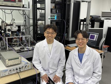
< Photo 1. Dr. Moojune Song (left) and Professor Kab-Jin Kim (right) of KAIST Department of Physics >
In simple terms, the researchers developed a special chip that synchronizes light and internal magnetic vibrations (magnons), enabling the transmission of phase information between distant magnets. They succeeded in observing and controlling interference between multiple signals in real time. This marks the first experimental evidence that magnets can serve as key components in quantum computing, serving as a pivotal step toward magnet-based quantum platforms.
The N and S poles of a magnet stem from the spin of electrons inside atoms. When many atoms align, their collective spin vibrations create a quantum particle known as a “magnon.”
Magnons are especially promising because of their nonreciprocal nature—they can carry information in only one direction, which makes them suitable for quantum noise isolation in compact quantum chips. They can also couple with both light and microwaves, enabling the potential for long-distance quantum communication over tens of kilometers.
Moreover, using special materials like antiferromagnets could allow quantum computers to operate at terahertz (THz) frequencies, far surpassing today’s hardware limitations, and possibly enabling room-temperature quantum computing without the need for bulky cryogenic equipment.
To build such a system, however, one must be able to transmit, measure, and control the phase information of magnons—the starting point and propagation of their waveforms—in real time. This had not been achieved until now.
< Figure 1. Superconducting Circuit-Based Magnon-Photon Hybrid System. (a) Schematic diagram of the device. A NbN superconducting resonator circuit fabricated on a silicon substrate is coupled with spherical YIG magnets (250 μm diameter), and magnons are generated and measured in real-time via a vertical antenna. (b) Photograph of the actual device. The distance between the two YIG spheres is 12 mm, a distance at which they cannot influence each other without the superconducting circuit. >
Professor Kim’s team used two tiny magnetic spheres made of Yttrium Iron Garnet (YIG) placed 12 mm apart with a superconducting resonator in between—similar to those used in quantum processors by Google and IBM. They input pulses into one magnet and successfully observed lossless transmission of magnon vibrations to the second magnet via the superconducting circuit.
They confirmed that from single nanosecond pulses to four microwave pulses, the magnon vibrations maintained their phase information and demonstrated predictable constructive or destructive interference in real time—known as coherent interference.
By adjusting the pulse frequencies and their intervals, the researchers could also freely control the interference patterns of magnons, effectively showing for the first time that electrical signals can be used to manipulate magnonic quantum states.
This work demonstrated that quantum gate operations using multiple pulses—a fundamental technique in quantum information processing—can be implemented using a hybrid system of magnetic materials and superconducting circuits. This opens the door for the practical use of magnet-based quantum devices.
< Figure 2. Experimental Data. (a) Measurement results of magnon-magnon band anticrossing via continuous wave measurement, showing the formation of a strong coupling hybrid system. (b) Magnon pulse exchange oscillation phenomenon between YIG spheres upon single pulse application. It can be seen that magnon information is coherently transmitted at regular time intervals through the superconducting circuit. (c,d) Magnon interference phenomenon upon dual pulse application. The magnon information state can be arbitrarily controlled by adjusting the time interval and carrier frequency between pulses. >
Professor Kab-Jin Kim stated, “This project began with a bold, even unconventional idea proposed to the Global Singularity Research Program: ‘What if we could build a quantum computer with magnets?’ The journey has been fascinating, and this study not only opens a new field of quantum spintronics, but also marks a turning point in developing high-efficiency quantum information processing devices.”
The research was co-led by postdoctoral researcher Moojune Song (KAIST), Dr. Yi Li and Dr. Valentine Novosad from Argonne National Lab, and Prof. Axel Hoffmann’s team at UIUC. The results were published in Nature Communications on April 17 and npj Spintronics on April 1, 2025.
Paper 1: Single-shot magnon interference in a magnon-superconducting-resonator hybrid circuit, Nat. Commun. 16, 3649 (2025)
DOI: https://doi.org/10.1038/s41467-025-58482-2
Paper 2: Single-shot electrical detection of short-wavelength magnon pulse transmission in a magnonic ultra-thin-film waveguide, npj Spintronics 3, 12 (2025)
DOI: https://doi.org/10.1038/s44306-025-00072-5
The research was supported by KAIST’s Global Singularity Research Initiative, the National Research Foundation of Korea (including the Mid-Career Researcher, Leading Research Center, and Quantum Information Science Human Resource Development programs), and the U.S. Department of Energy.
2025.06.12 View 11576
KAIST Turns an Unprecedented Idea into Reality: Quantum Computing with Magnets
What started as an idea under KAIST’s Global Singularity Research Project—"Can we build a quantum computer using magnets?"—has now become a scientific reality. A KAIST-led international research team has successfully demonstrated a core quantum computing technology using magnetic materials (ferromagnets) for the first time in the world.
KAIST (represented by President Kwang-Hyung Lee) announced on the 6th of May that a team led by Professor Kab-Jin Kim from the Department of Physics, in collaboration with the Argonne National Laboratory and the University of Illinois Urbana-Champaign (UIUC), has developed a “photon-magnon hybrid chip” and successfully implemented real-time, multi-pulse interference using magnetic materials—marking a global first.
< Photo 1. Dr. Moojune Song (left) and Professor Kab-Jin Kim (right) of KAIST Department of Physics >
In simple terms, the researchers developed a special chip that synchronizes light and internal magnetic vibrations (magnons), enabling the transmission of phase information between distant magnets. They succeeded in observing and controlling interference between multiple signals in real time. This marks the first experimental evidence that magnets can serve as key components in quantum computing, serving as a pivotal step toward magnet-based quantum platforms.
The N and S poles of a magnet stem from the spin of electrons inside atoms. When many atoms align, their collective spin vibrations create a quantum particle known as a “magnon.”
Magnons are especially promising because of their nonreciprocal nature—they can carry information in only one direction, which makes them suitable for quantum noise isolation in compact quantum chips. They can also couple with both light and microwaves, enabling the potential for long-distance quantum communication over tens of kilometers.
Moreover, using special materials like antiferromagnets could allow quantum computers to operate at terahertz (THz) frequencies, far surpassing today’s hardware limitations, and possibly enabling room-temperature quantum computing without the need for bulky cryogenic equipment.
To build such a system, however, one must be able to transmit, measure, and control the phase information of magnons—the starting point and propagation of their waveforms—in real time. This had not been achieved until now.
< Figure 1. Superconducting Circuit-Based Magnon-Photon Hybrid System. (a) Schematic diagram of the device. A NbN superconducting resonator circuit fabricated on a silicon substrate is coupled with spherical YIG magnets (250 μm diameter), and magnons are generated and measured in real-time via a vertical antenna. (b) Photograph of the actual device. The distance between the two YIG spheres is 12 mm, a distance at which they cannot influence each other without the superconducting circuit. >
Professor Kim’s team used two tiny magnetic spheres made of Yttrium Iron Garnet (YIG) placed 12 mm apart with a superconducting resonator in between—similar to those used in quantum processors by Google and IBM. They input pulses into one magnet and successfully observed lossless transmission of magnon vibrations to the second magnet via the superconducting circuit.
They confirmed that from single nanosecond pulses to four microwave pulses, the magnon vibrations maintained their phase information and demonstrated predictable constructive or destructive interference in real time—known as coherent interference.
By adjusting the pulse frequencies and their intervals, the researchers could also freely control the interference patterns of magnons, effectively showing for the first time that electrical signals can be used to manipulate magnonic quantum states.
This work demonstrated that quantum gate operations using multiple pulses—a fundamental technique in quantum information processing—can be implemented using a hybrid system of magnetic materials and superconducting circuits. This opens the door for the practical use of magnet-based quantum devices.
< Figure 2. Experimental Data. (a) Measurement results of magnon-magnon band anticrossing via continuous wave measurement, showing the formation of a strong coupling hybrid system. (b) Magnon pulse exchange oscillation phenomenon between YIG spheres upon single pulse application. It can be seen that magnon information is coherently transmitted at regular time intervals through the superconducting circuit. (c,d) Magnon interference phenomenon upon dual pulse application. The magnon information state can be arbitrarily controlled by adjusting the time interval and carrier frequency between pulses. >
Professor Kab-Jin Kim stated, “This project began with a bold, even unconventional idea proposed to the Global Singularity Research Program: ‘What if we could build a quantum computer with magnets?’ The journey has been fascinating, and this study not only opens a new field of quantum spintronics, but also marks a turning point in developing high-efficiency quantum information processing devices.”
The research was co-led by postdoctoral researcher Moojune Song (KAIST), Dr. Yi Li and Dr. Valentine Novosad from Argonne National Lab, and Prof. Axel Hoffmann’s team at UIUC. The results were published in Nature Communications on April 17 and npj Spintronics on April 1, 2025.
Paper 1: Single-shot magnon interference in a magnon-superconducting-resonator hybrid circuit, Nat. Commun. 16, 3649 (2025)
DOI: https://doi.org/10.1038/s41467-025-58482-2
Paper 2: Single-shot electrical detection of short-wavelength magnon pulse transmission in a magnonic ultra-thin-film waveguide, npj Spintronics 3, 12 (2025)
DOI: https://doi.org/10.1038/s44306-025-00072-5
The research was supported by KAIST’s Global Singularity Research Initiative, the National Research Foundation of Korea (including the Mid-Career Researcher, Leading Research Center, and Quantum Information Science Human Resource Development programs), and the U.S. Department of Energy.
2025.06.12 View 11576 -
 Decoding Fear: KAIST Identifies An Affective Brain Circuit Crucial for Fear Memory Formation by Non-nociceptive Threat Stimulus
Fear memories can form in the brain following exposure to threatening situations such as natural disasters, accidents, or violence. When these memories become excessive or distorted, they can lead to severe mental health disorders, including post-traumatic stress disorder (PTSD), anxiety disorders, and depression. However, the mechanisms underlying fear memory formation triggered by affective pain rather than direct physical pain have remained largely unexplored – until now.
A KAIST research team has identified, for the first time, a brain circuit specifically responsible for forming fear memories in the absence of physical pain, marking a significant advance in understanding how psychological distress is processed and drives fear memory formation in the brain. This discovery opens the door to the development of targeted treatments for trauma-related conditions by addressing the underlying neural pathways.
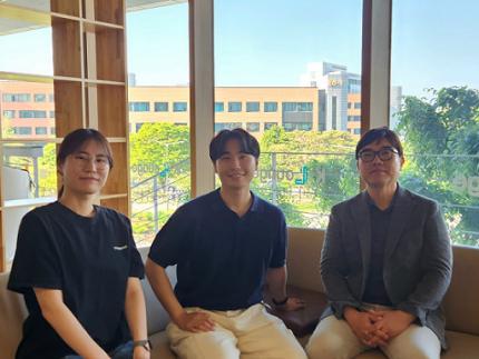
< Photo 1. (from left) Professor Jin-Hee Han, Dr. Junho Han and Ph.D. Candidate Boin Suh of the Department of Biological Sciences >
KAIST (President Kwang-Hyung Lee) announced on May 15th that the research team led by Professor Jin-Hee Han in the Department of Biological Sciences has identified the pIC-PBN circuit*, a key neural pathway involved in forming fear memories triggered by psychological threats in the absence of sensory pain. This groundbreaking work was conducted through experiments with mice.*pIC–PBN circuit: A newly identified descending neural pathway from the posterior insular cortex (pIC) to the parabrachial nucleus (PBN), specialized for transmitting psychological threat information.
Traditionally, the lateral parabrachial nucleus (PBN) has been recognized as a critical part of the ascending pain pathway, receiving pain signals from the spinal cord. However, this study reveals a previously unknown role for the PBN in processing fear induced by non-painful psychological stimuli, fundamentally changing our understanding of its function in the brain.
This work is considered the first experimental evidence that 'emotional distress' and 'physical pain' are processed through different neural circuits to form fear memories, making it a significant contribution to the field of neuroscience. It clearly demonstrates the existence of a dedicated pathway (pIC-PBN) for transmitting emotional distress.
The study's first author, Dr. Junho Han, shared the personal motivation behind this research: “Our dog, Lego, is afraid of motorcycles. He never actually crashed into one, but ever since having a traumatizing event of having a motorbike almost run into him, just hearing the sound now triggers a fearful response. Humans react similarly – even if you didn’t have a personal experience of being involved in an accident, a near-miss or exposure to alarming media can create lasting fear memories, which may eventually lead to PTSD.”
He continued, “Until now, fear memory research has mainly relied on experimental models involving physical pain. However, much of real-world human fears arise from psychological threats, rather than from direct physical harm. Despite this, little was known about the brain circuits responsible for processing these psychological threats that can drive fear memory formation.”
To investigate this, the research team developed a novel fear conditioning model that utilizes visual threat stimuli instead of electrical shocks. In this model, mice were exposed to a rapidly expanding visual disk on a ceiling screen, simulating the threat of an approaching predator. This approach allowed the team to demonstrate that fear memories can form in response to a non-nociceptive, psychological threat alone, without the need for physical pain.
< Figure 1. Artificial activation of the posterior insular cortex (pIC) to lateral parabrachial nucleus (PBN) neural circuit induces anxiety-like behaviors and fear memory formation in mice. >
Using advanced chemogenetic and optogenetic techniques, the team precisely controlled neuronal activity, revealing that the lateral parabrachial nucleus (PBN) is essential to form fear memories in response to visual threats. They further traced the origin of these signals to the posterior insular cortex (pIC), a region known to process negative emotions and pain, confirming a direct connection between the two areas.
The study also showed that inhibiting the pIC–PBN circuit significantly reduced fear memory formation in response to visual threats, without affecting innate fear responses or physical pain-based learning. Conversely, artificially activating this circuit alone was sufficient to drive fear memory formation, confirming its role as a key pathway for processing psychological threat information.
< Figure 2. Schematic diagram of brain neural circuits transmitting emotional & physical pain threat signals. Visual threat stimuli do not involve physical pain but can create an anxious state and form fear memory through the affective pain signaling pathway. >
Professor Jin-Hee Han commented, “This study lays an important foundation for understanding how emotional distress-based mental disorders, such as PTSD, panic disorder, and anxiety disorder, develop, and opens new possibilities for targeted treatment approaches.”
The findings, authored by Dr. Junho Han (first author), Ph.D. candidate Boin Suh (second author), and Dr. Jin-Hee Han (corresponding author) of the Department of Biological Sciences, were published online in the international journal Science Advances on May 9, 2025.※ Paper Title: A top-down insular cortex circuit crucial for non-nociceptive fear learning. Science Advances (https://doi.org/10.1101/2024.10.14.618356)※ Author Information: Junho Han (first author), Boin Suh (second author), and Jin-Hee Han (corresponding author)
This research was supported by grants from the National Research Foundation of Korea (NRF-2022M3E5E8081183 and NRF-2017M3C7A1031322).
2025.05.15 View 9489
Decoding Fear: KAIST Identifies An Affective Brain Circuit Crucial for Fear Memory Formation by Non-nociceptive Threat Stimulus
Fear memories can form in the brain following exposure to threatening situations such as natural disasters, accidents, or violence. When these memories become excessive or distorted, they can lead to severe mental health disorders, including post-traumatic stress disorder (PTSD), anxiety disorders, and depression. However, the mechanisms underlying fear memory formation triggered by affective pain rather than direct physical pain have remained largely unexplored – until now.
A KAIST research team has identified, for the first time, a brain circuit specifically responsible for forming fear memories in the absence of physical pain, marking a significant advance in understanding how psychological distress is processed and drives fear memory formation in the brain. This discovery opens the door to the development of targeted treatments for trauma-related conditions by addressing the underlying neural pathways.
< Photo 1. (from left) Professor Jin-Hee Han, Dr. Junho Han and Ph.D. Candidate Boin Suh of the Department of Biological Sciences >
KAIST (President Kwang-Hyung Lee) announced on May 15th that the research team led by Professor Jin-Hee Han in the Department of Biological Sciences has identified the pIC-PBN circuit*, a key neural pathway involved in forming fear memories triggered by psychological threats in the absence of sensory pain. This groundbreaking work was conducted through experiments with mice.*pIC–PBN circuit: A newly identified descending neural pathway from the posterior insular cortex (pIC) to the parabrachial nucleus (PBN), specialized for transmitting psychological threat information.
Traditionally, the lateral parabrachial nucleus (PBN) has been recognized as a critical part of the ascending pain pathway, receiving pain signals from the spinal cord. However, this study reveals a previously unknown role for the PBN in processing fear induced by non-painful psychological stimuli, fundamentally changing our understanding of its function in the brain.
This work is considered the first experimental evidence that 'emotional distress' and 'physical pain' are processed through different neural circuits to form fear memories, making it a significant contribution to the field of neuroscience. It clearly demonstrates the existence of a dedicated pathway (pIC-PBN) for transmitting emotional distress.
The study's first author, Dr. Junho Han, shared the personal motivation behind this research: “Our dog, Lego, is afraid of motorcycles. He never actually crashed into one, but ever since having a traumatizing event of having a motorbike almost run into him, just hearing the sound now triggers a fearful response. Humans react similarly – even if you didn’t have a personal experience of being involved in an accident, a near-miss or exposure to alarming media can create lasting fear memories, which may eventually lead to PTSD.”
He continued, “Until now, fear memory research has mainly relied on experimental models involving physical pain. However, much of real-world human fears arise from psychological threats, rather than from direct physical harm. Despite this, little was known about the brain circuits responsible for processing these psychological threats that can drive fear memory formation.”
To investigate this, the research team developed a novel fear conditioning model that utilizes visual threat stimuli instead of electrical shocks. In this model, mice were exposed to a rapidly expanding visual disk on a ceiling screen, simulating the threat of an approaching predator. This approach allowed the team to demonstrate that fear memories can form in response to a non-nociceptive, psychological threat alone, without the need for physical pain.
< Figure 1. Artificial activation of the posterior insular cortex (pIC) to lateral parabrachial nucleus (PBN) neural circuit induces anxiety-like behaviors and fear memory formation in mice. >
Using advanced chemogenetic and optogenetic techniques, the team precisely controlled neuronal activity, revealing that the lateral parabrachial nucleus (PBN) is essential to form fear memories in response to visual threats. They further traced the origin of these signals to the posterior insular cortex (pIC), a region known to process negative emotions and pain, confirming a direct connection between the two areas.
The study also showed that inhibiting the pIC–PBN circuit significantly reduced fear memory formation in response to visual threats, without affecting innate fear responses or physical pain-based learning. Conversely, artificially activating this circuit alone was sufficient to drive fear memory formation, confirming its role as a key pathway for processing psychological threat information.
< Figure 2. Schematic diagram of brain neural circuits transmitting emotional & physical pain threat signals. Visual threat stimuli do not involve physical pain but can create an anxious state and form fear memory through the affective pain signaling pathway. >
Professor Jin-Hee Han commented, “This study lays an important foundation for understanding how emotional distress-based mental disorders, such as PTSD, panic disorder, and anxiety disorder, develop, and opens new possibilities for targeted treatment approaches.”
The findings, authored by Dr. Junho Han (first author), Ph.D. candidate Boin Suh (second author), and Dr. Jin-Hee Han (corresponding author) of the Department of Biological Sciences, were published online in the international journal Science Advances on May 9, 2025.※ Paper Title: A top-down insular cortex circuit crucial for non-nociceptive fear learning. Science Advances (https://doi.org/10.1101/2024.10.14.618356)※ Author Information: Junho Han (first author), Boin Suh (second author), and Jin-Hee Han (corresponding author)
This research was supported by grants from the National Research Foundation of Korea (NRF-2022M3E5E8081183 and NRF-2017M3C7A1031322).
2025.05.15 View 9489 -
 KAIST researchers discovers the neural circuit that reacts to alarm clock
KAIST (President Kwang Hyung Lee) announced on the 20th that a research team led by Professor Daesoo Kim of the Department of Brain and Cognitive Sciences and Dr. Jeongjin Kim 's team from the Korea Institute of Science and Technology (KIST) have identified the principle of awakening animals by responding to sounds even while sleeping.
Sleep is a very important physiological process that organizes brain activity and maintains health. During sleep, the function of sensory nerves is blocked, so the ability to detect danger in the proximity is reduced. However, many animals detect approaching predators and respond even while sleeping. Scientists thought that animals ready for danger by alternating between deep sleep and light sleep.
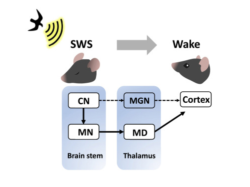
A research team led by Professor Daesoo Kim at KAIST discovered that animals have neural circuits that respond to sounds even during deep sleep. While awake, the medial geniculate thalamus responds to sounds, but during deep sleep, or Non-REM sleep, the Mediodorsal thalamus responds to sounds to wake up the brain.
As a result of the study, when the rats fell into deep sleep, the nerves of the medial geniculate thalamus were also sleeping, but the nerves of mediodorsal thalamus were awake and responded immediately to sounds. In addition, it was observed that when mediodorsal thalamus was inhibited, the rats could not wake up even when a sound was heard, and when the mediodorsal thalamus was stimulated, the rats woke up within a few seconds without sound.
This is the first study to show that sleep and wakefulness can transmit auditory signals through different neural circuits, and was reported in the international journal, Current Biology on February 7, and was highlighted by Nature. (https://www.nature.com/articles/d41586-023-00354-0)
Professor Daesoo Kim explained, “The findings of this study can used in developing digital healthcare technologies to be used to improve understanding of disorders of senses and wakefulness seen in various brain diseases and to control the senses in the future.”
This research was carried out with the support from the National Research Foundation of Korea's Mid-Career Research Foundation Program.
Figure 1. Traditionally, sound signals were thought to be propagated from the auditory nerve to the auditory thalamus. However, while in slow-wave sleep, the auditory nerve sends sound signals to the mediodorsal thalamic neurons via the brainstem nerve to induce arousal in the brain.
Figure 2. GRIK4 dorsomedial nerve in response to sound stimulation. The awakening effect is induced as the activity of the GRIK4 dorsal medial nerve increases based on the time when sound stimulation is given.
2023.03.03 View 10311
KAIST researchers discovers the neural circuit that reacts to alarm clock
KAIST (President Kwang Hyung Lee) announced on the 20th that a research team led by Professor Daesoo Kim of the Department of Brain and Cognitive Sciences and Dr. Jeongjin Kim 's team from the Korea Institute of Science and Technology (KIST) have identified the principle of awakening animals by responding to sounds even while sleeping.
Sleep is a very important physiological process that organizes brain activity and maintains health. During sleep, the function of sensory nerves is blocked, so the ability to detect danger in the proximity is reduced. However, many animals detect approaching predators and respond even while sleeping. Scientists thought that animals ready for danger by alternating between deep sleep and light sleep.
A research team led by Professor Daesoo Kim at KAIST discovered that animals have neural circuits that respond to sounds even during deep sleep. While awake, the medial geniculate thalamus responds to sounds, but during deep sleep, or Non-REM sleep, the Mediodorsal thalamus responds to sounds to wake up the brain.
As a result of the study, when the rats fell into deep sleep, the nerves of the medial geniculate thalamus were also sleeping, but the nerves of mediodorsal thalamus were awake and responded immediately to sounds. In addition, it was observed that when mediodorsal thalamus was inhibited, the rats could not wake up even when a sound was heard, and when the mediodorsal thalamus was stimulated, the rats woke up within a few seconds without sound.
This is the first study to show that sleep and wakefulness can transmit auditory signals through different neural circuits, and was reported in the international journal, Current Biology on February 7, and was highlighted by Nature. (https://www.nature.com/articles/d41586-023-00354-0)
Professor Daesoo Kim explained, “The findings of this study can used in developing digital healthcare technologies to be used to improve understanding of disorders of senses and wakefulness seen in various brain diseases and to control the senses in the future.”
This research was carried out with the support from the National Research Foundation of Korea's Mid-Career Research Foundation Program.
Figure 1. Traditionally, sound signals were thought to be propagated from the auditory nerve to the auditory thalamus. However, while in slow-wave sleep, the auditory nerve sends sound signals to the mediodorsal thalamic neurons via the brainstem nerve to induce arousal in the brain.
Figure 2. GRIK4 dorsomedial nerve in response to sound stimulation. The awakening effect is induced as the activity of the GRIK4 dorsal medial nerve increases based on the time when sound stimulation is given.
2023.03.03 View 10311 -
 Neuromorphic Memory Device Simulates Neurons and Synapses
Simultaneous emulation of neuronal and synaptic properties promotes the development of brain-like artificial intelligence
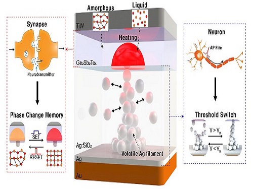
Researchers have reported a nano-sized neuromorphic memory device that emulates neurons and synapses simultaneously in a unit cell, another step toward completing the goal of neuromorphic computing designed to rigorously mimic the human brain with semiconductor devices.
Neuromorphic computing aims to realize artificial intelligence (AI) by mimicking the mechanisms of neurons and synapses that make up the human brain. Inspired by the cognitive functions of the human brain that current computers cannot provide, neuromorphic devices have been widely investigated. However, current Complementary Metal-Oxide Semiconductor (CMOS)-based neuromorphic circuits simply connect artificial neurons and synapses without synergistic interactions, and the concomitant implementation of neurons and synapses still remains a challenge. To address these issues, a research team led by Professor Keon Jae Lee from the Department of Materials Science and Engineering implemented the biological working mechanisms of humans by introducing the neuron-synapse interactions in a single memory cell, rather than the conventional approach of electrically connecting artificial neuronal and synaptic devices.
Similar to commercial graphics cards, the artificial synaptic devices previously studied often used to accelerate parallel computations, which shows clear differences from the operational mechanisms of the human brain. The research team implemented the synergistic interactions between neurons and synapses in the neuromorphic memory device, emulating the mechanisms of the biological neural network. In addition, the developed neuromorphic device can replace complex CMOS neuron circuits with a single device, providing high scalability and cost efficiency.
The human brain consists of a complex network of 100 billion neurons and 100 trillion synapses. The functions and structures of neurons and synapses can flexibly change according to the external stimuli, adapting to the surrounding environment. The research team developed a neuromorphic device in which short-term and long-term memories coexist using volatile and non-volatile memory devices that mimic the characteristics of neurons and synapses, respectively. A threshold switch device is used as volatile memory and phase-change memory is used as a non-volatile device. Two thin-film devices are integrated without intermediate electrodes, implementing the functional adaptability of neurons and synapses in the neuromorphic memory.
Professor Keon Jae Lee explained, "Neurons and synapses interact with each other to establish cognitive functions such as memory and learning, so simulating both is an essential element for brain-inspired artificial intelligence. The developed neuromorphic memory device also mimics the retraining effect that allows quick learning of the forgotten information by implementing a positive feedback effect between neurons and synapses.”
This result entitled “Simultaneous emulation of synaptic and intrinsic plasticity using a memristive synapse” was published in the May 19, 2022 issue of Nature Communications.
-Publication:Sang Hyun Sung, Tae Jin Kim, Hyera Shin, Tae Hong Im, and Keon Jae Lee (2022) “Simultaneous emulation of synaptic and intrinsic plasticity using a memristive synapse,” Nature Communications May 19, 2022 (DOI: 10.1038/s41467-022-30432-2)
-Profile:Professor Keon Jae Leehttp://fand.kaist.ac.kr
Department of Materials Science and EngineeringKAIST
2022.05.20 View 22217
Neuromorphic Memory Device Simulates Neurons and Synapses
Simultaneous emulation of neuronal and synaptic properties promotes the development of brain-like artificial intelligence
Researchers have reported a nano-sized neuromorphic memory device that emulates neurons and synapses simultaneously in a unit cell, another step toward completing the goal of neuromorphic computing designed to rigorously mimic the human brain with semiconductor devices.
Neuromorphic computing aims to realize artificial intelligence (AI) by mimicking the mechanisms of neurons and synapses that make up the human brain. Inspired by the cognitive functions of the human brain that current computers cannot provide, neuromorphic devices have been widely investigated. However, current Complementary Metal-Oxide Semiconductor (CMOS)-based neuromorphic circuits simply connect artificial neurons and synapses without synergistic interactions, and the concomitant implementation of neurons and synapses still remains a challenge. To address these issues, a research team led by Professor Keon Jae Lee from the Department of Materials Science and Engineering implemented the biological working mechanisms of humans by introducing the neuron-synapse interactions in a single memory cell, rather than the conventional approach of electrically connecting artificial neuronal and synaptic devices.
Similar to commercial graphics cards, the artificial synaptic devices previously studied often used to accelerate parallel computations, which shows clear differences from the operational mechanisms of the human brain. The research team implemented the synergistic interactions between neurons and synapses in the neuromorphic memory device, emulating the mechanisms of the biological neural network. In addition, the developed neuromorphic device can replace complex CMOS neuron circuits with a single device, providing high scalability and cost efficiency.
The human brain consists of a complex network of 100 billion neurons and 100 trillion synapses. The functions and structures of neurons and synapses can flexibly change according to the external stimuli, adapting to the surrounding environment. The research team developed a neuromorphic device in which short-term and long-term memories coexist using volatile and non-volatile memory devices that mimic the characteristics of neurons and synapses, respectively. A threshold switch device is used as volatile memory and phase-change memory is used as a non-volatile device. Two thin-film devices are integrated without intermediate electrodes, implementing the functional adaptability of neurons and synapses in the neuromorphic memory.
Professor Keon Jae Lee explained, "Neurons and synapses interact with each other to establish cognitive functions such as memory and learning, so simulating both is an essential element for brain-inspired artificial intelligence. The developed neuromorphic memory device also mimics the retraining effect that allows quick learning of the forgotten information by implementing a positive feedback effect between neurons and synapses.”
This result entitled “Simultaneous emulation of synaptic and intrinsic plasticity using a memristive synapse” was published in the May 19, 2022 issue of Nature Communications.
-Publication:Sang Hyun Sung, Tae Jin Kim, Hyera Shin, Tae Hong Im, and Keon Jae Lee (2022) “Simultaneous emulation of synaptic and intrinsic plasticity using a memristive synapse,” Nature Communications May 19, 2022 (DOI: 10.1038/s41467-022-30432-2)
-Profile:Professor Keon Jae Leehttp://fand.kaist.ac.kr
Department of Materials Science and EngineeringKAIST
2022.05.20 View 22217 -
 Energy-Efficient AI Hardware Technology Via a Brain-Inspired Stashing System
Researchers demonstrate neuromodulation-inspired stashing system for the energy-efficient learning of a spiking neural network using a self-rectifying memristor array
Researchers have proposed a novel system inspired by the neuromodulation of the brain, referred to as a ‘stashing system,’ that requires less energy consumption. The research group led by Professor Kyung Min Kim from the Department of Materials Science and Engineering has developed a technology that can efficiently handle mathematical operations for artificial intelligence by imitating the continuous changes in the topology of the neural network according to the situation. The human brain changes its neural topology in real time, learning to store or recall memories as needed. The research group presented a new artificial intelligence learning method that directly implements these neural coordination circuit configurations.
Research on artificial intelligence is becoming very active, and the development of artificial intelligence-based electronic devices and product releases are accelerating, especially in the Fourth Industrial Revolution age. To implement artificial intelligence in electronic devices, customized hardware development should also be supported. However most electronic devices for artificial intelligence require high power consumption and highly integrated memory arrays for large-scale tasks. It has been challenging to solve these power consumption and integration limitations, and efforts have been made to find out how the human brain solves problems.
To prove the efficiency of the developed technology, the research group created artificial neural network hardware equipped with a self-rectifying synaptic array and algorithm called a ‘stashing system’ that was developed to conduct artificial intelligence learning. As a result, it was able to reduce energy by 37% within the stashing system without any accuracy degradation. This result proves that emulating the neuromodulation in humans is possible.
Professor Kim said, "In this study, we implemented the learning method of the human brain with only a simple circuit composition and through this we were able to reduce the energy needed by nearly 40 percent.”
This neuromodulation-inspired stashing system that mimics the brain’s neural activity is compatible with existing electronic devices and commercialized semiconductor hardware. It is expected to be used in the design of next-generation semiconductor chips for artificial intelligence.
This study was published in Advanced Functional Materials in March 2022 and supported by KAIST, the National Research Foundation of Korea, the National NanoFab Center, and SK Hynix.
-Publication:
Woon Hyung Cheong, Jae Bum Jeon†, Jae Hyun In, Geunyoung Kim, Hanchan Song, Janho An, Juseong Park, Young Seok Kim, Cheol Seong Hwang, and Kyung Min Kim (2022)
“Demonstration of Neuromodulation-inspired Stashing System for Energy-efficient Learning of Spiking Neural Network using a Self-Rectifying Memristor Array,” Advanced FunctionalMaterials March 31, 2022 (DOI: 10.1002/adfm.202200337)
-Profile:
Professor Kyung Min Kimhttp://semi.kaist.ac.kr https://scholar.google.com/citations?user=BGw8yDYAAAAJ&hl=ko
Department of Materials Science and EngineeringKAIST
2022.05.18 View 17340
Energy-Efficient AI Hardware Technology Via a Brain-Inspired Stashing System
Researchers demonstrate neuromodulation-inspired stashing system for the energy-efficient learning of a spiking neural network using a self-rectifying memristor array
Researchers have proposed a novel system inspired by the neuromodulation of the brain, referred to as a ‘stashing system,’ that requires less energy consumption. The research group led by Professor Kyung Min Kim from the Department of Materials Science and Engineering has developed a technology that can efficiently handle mathematical operations for artificial intelligence by imitating the continuous changes in the topology of the neural network according to the situation. The human brain changes its neural topology in real time, learning to store or recall memories as needed. The research group presented a new artificial intelligence learning method that directly implements these neural coordination circuit configurations.
Research on artificial intelligence is becoming very active, and the development of artificial intelligence-based electronic devices and product releases are accelerating, especially in the Fourth Industrial Revolution age. To implement artificial intelligence in electronic devices, customized hardware development should also be supported. However most electronic devices for artificial intelligence require high power consumption and highly integrated memory arrays for large-scale tasks. It has been challenging to solve these power consumption and integration limitations, and efforts have been made to find out how the human brain solves problems.
To prove the efficiency of the developed technology, the research group created artificial neural network hardware equipped with a self-rectifying synaptic array and algorithm called a ‘stashing system’ that was developed to conduct artificial intelligence learning. As a result, it was able to reduce energy by 37% within the stashing system without any accuracy degradation. This result proves that emulating the neuromodulation in humans is possible.
Professor Kim said, "In this study, we implemented the learning method of the human brain with only a simple circuit composition and through this we were able to reduce the energy needed by nearly 40 percent.”
This neuromodulation-inspired stashing system that mimics the brain’s neural activity is compatible with existing electronic devices and commercialized semiconductor hardware. It is expected to be used in the design of next-generation semiconductor chips for artificial intelligence.
This study was published in Advanced Functional Materials in March 2022 and supported by KAIST, the National Research Foundation of Korea, the National NanoFab Center, and SK Hynix.
-Publication:
Woon Hyung Cheong, Jae Bum Jeon†, Jae Hyun In, Geunyoung Kim, Hanchan Song, Janho An, Juseong Park, Young Seok Kim, Cheol Seong Hwang, and Kyung Min Kim (2022)
“Demonstration of Neuromodulation-inspired Stashing System for Energy-efficient Learning of Spiking Neural Network using a Self-Rectifying Memristor Array,” Advanced FunctionalMaterials March 31, 2022 (DOI: 10.1002/adfm.202200337)
-Profile:
Professor Kyung Min Kimhttp://semi.kaist.ac.kr https://scholar.google.com/citations?user=BGw8yDYAAAAJ&hl=ko
Department of Materials Science and EngineeringKAIST
2022.05.18 View 17340 -
 A Team of Three PhD Candidates Wins the Korea Semiconductor Design Contest
“We felt a sense of responsibility to help the nation advance its semiconductor design technology”
A CMOS (complementary metal-oxide semiconductor)-based “ultra-low noise signal chip” for 6G communications designed by three PhD candidates at the KAIST School of Electrical Engineering won the Presidential Award at the 22nd Korea Semiconductor Design Contest.
The winners are PhD candidates Sun-Eui Park, Yoon-Seo Cho, and Ju-Eun Bang from the Integrated Circuits and System Lab run by Professor Jaehyouk Choi. The contest, which is hosted by the Ministry of Trade, Industry and Energy and the Korea Semiconductors Industry Association, is one of the top national semiconductor design contests for college students.
Park said the team felt a sense of responsibility to help advance semiconductor design technology in Korea when deciding to participate the contest. The team expressed deep gratitude to Professor Choi for guiding their research on 6G communications.
“Our colleagues from other labs and seniors who already graduated helped us a great deal, so we owe them a lot,” explained Park. Cho added that their hard work finally got recognized and that acknowledgement pushes her to move forward with her research. Meanwhile, Bang said she is delighted to see that many people seem to be interested in her research topic.
Research for 6G is attempting to reach 1 tera bps (Tbps), 50 times faster than 5G communications with transmission speeds of up to 20 gigabytes. In general, the wider the communication frequency band, the higher the data transmission speed. Thus, the use of frequency bands above 100 gigahertz is essential for delivering high data transmission speeds for 6G communications.
However, it remains a big challenge to make a precise benchmark signal that can be used as a carrier wave in a high frequency band. Despite the advantages of CMOS’s ultra-small and low-power design, it still has limitations at high frequency bands and its operating frequency. Thus, it was difficult to achieve a frequency band above 100 gigahertz.
To overcome these challenges, the three students introduced ultra-low noise signal generation technology that can support high-order modulation technologies. This technology is expected to contribute to increasing the price competitiveness and density of 6G communication chips that will be used in the future.
5G just got started in 2020 and still has long way to go for full commercialization. Nevertheless, many researchers have started preparing for 6G technology, targeting 2030 since a new cellular communication appears in every other decade.
Professor Choi said, “Generating ultra-high frequency signals in bands above 100 GHz with highly accurate timing is one of the key technologies for implementing 6G communication hardware. Our research is significant for the development of the world’s first semiconductor chip that will use the CMOS process to achieve noise performance of less than 80fs in a frequency band above 100 GHz.”
The team members plan to work as circuit designers in Korean semiconductor companies after graduation. “We will continue to research the development of signal generators on the topic of award-winning 6G. We would like to continue our research on high-speed circuit designs such as ultra-fast analog-to-digital converters,” Park added.
2021.11.30 View 15194
A Team of Three PhD Candidates Wins the Korea Semiconductor Design Contest
“We felt a sense of responsibility to help the nation advance its semiconductor design technology”
A CMOS (complementary metal-oxide semiconductor)-based “ultra-low noise signal chip” for 6G communications designed by three PhD candidates at the KAIST School of Electrical Engineering won the Presidential Award at the 22nd Korea Semiconductor Design Contest.
The winners are PhD candidates Sun-Eui Park, Yoon-Seo Cho, and Ju-Eun Bang from the Integrated Circuits and System Lab run by Professor Jaehyouk Choi. The contest, which is hosted by the Ministry of Trade, Industry and Energy and the Korea Semiconductors Industry Association, is one of the top national semiconductor design contests for college students.
Park said the team felt a sense of responsibility to help advance semiconductor design technology in Korea when deciding to participate the contest. The team expressed deep gratitude to Professor Choi for guiding their research on 6G communications.
“Our colleagues from other labs and seniors who already graduated helped us a great deal, so we owe them a lot,” explained Park. Cho added that their hard work finally got recognized and that acknowledgement pushes her to move forward with her research. Meanwhile, Bang said she is delighted to see that many people seem to be interested in her research topic.
Research for 6G is attempting to reach 1 tera bps (Tbps), 50 times faster than 5G communications with transmission speeds of up to 20 gigabytes. In general, the wider the communication frequency band, the higher the data transmission speed. Thus, the use of frequency bands above 100 gigahertz is essential for delivering high data transmission speeds for 6G communications.
However, it remains a big challenge to make a precise benchmark signal that can be used as a carrier wave in a high frequency band. Despite the advantages of CMOS’s ultra-small and low-power design, it still has limitations at high frequency bands and its operating frequency. Thus, it was difficult to achieve a frequency band above 100 gigahertz.
To overcome these challenges, the three students introduced ultra-low noise signal generation technology that can support high-order modulation technologies. This technology is expected to contribute to increasing the price competitiveness and density of 6G communication chips that will be used in the future.
5G just got started in 2020 and still has long way to go for full commercialization. Nevertheless, many researchers have started preparing for 6G technology, targeting 2030 since a new cellular communication appears in every other decade.
Professor Choi said, “Generating ultra-high frequency signals in bands above 100 GHz with highly accurate timing is one of the key technologies for implementing 6G communication hardware. Our research is significant for the development of the world’s first semiconductor chip that will use the CMOS process to achieve noise performance of less than 80fs in a frequency band above 100 GHz.”
The team members plan to work as circuit designers in Korean semiconductor companies after graduation. “We will continue to research the development of signal generators on the topic of award-winning 6G. We would like to continue our research on high-speed circuit designs such as ultra-fast analog-to-digital converters,” Park added.
2021.11.30 View 15194 -
 Scientists Develop Wireless Networks that Allow Brain Circuits to Be Controlled Remotely through the Internet
Wireless implantable devices and IoT could manipulate the brains of animals from anywhere around the world due to their minimalistic hardware, low setup cost, ease of use, and customizable versatility
A new study shows that researchers can remotely control the brain circuits of numerous animals simultaneously and independently through the internet. The scientists believe this newly developed technology can speed up brain research and various neuroscience studies to uncover basic brain functions as well as the underpinnings of various neuropsychiatric and neurological disorders.
A multidisciplinary team of researchers at KAIST, Washington University in St. Louis, and the University of Colorado, Boulder, created a wireless ecosystem with its own wireless implantable devices and Internet of Things (IoT) infrastructure to enable high-throughput neuroscience experiments over the internet. This innovative technology could enable scientists to manipulate the brains of animals from anywhere around the world. The study was published in the journal Nature Biomedical Engineering on November 25
“This novel technology is highly versatile and adaptive. It can remotely control numerous neural implants and laboratory tools in real-time or in a scheduled way without direct human interactions,” said Professor Jae-Woong Jeong of the School of Electrical Engineering at KAIST and a senior author of the study. “These wireless neural devices and equipment integrated with IoT technology have enormous potential for science and medicine.”
The wireless ecosystem only requires a mini-computer that can be purchased for under $45, which connects to the internet and communicates with wireless multifunctional brain probes or other types of conventional laboratory equipment using IoT control modules. By optimally integrating the versatility and modular construction of both unique IoT hardware and software within a single ecosystem, this wireless technology offers new applications that have not been demonstrated before by a single standalone technology. This includes, but is not limited to minimalistic hardware, global remote access, selective and scheduled experiments, customizable automation, and high-throughput scalability.
“As long as researchers have internet access, they are able to trigger, customize, stop, validate, and store the outcomes of large experiments at any time and from anywhere in the world. They can remotely perform large-scale neuroscience experiments in animals deployed in multiple countries,” said one of the lead authors, Dr. Raza Qazi, a researcher with KAIST and the University of Colorado, Boulder. “The low cost of this system allows it to be easily adopted and can further fuel innovation across many laboratories,” Dr. Qazi added.
One of the significant advantages of this IoT neurotechnology is its ability to be mass deployed across the globe due to its minimalistic hardware, low setup cost, ease of use, and customizable versatility. Scientists across the world can quickly implement this technology within their existing laboratories with minimal budget concerns to achieve globally remote access, scalable experimental automation, or both, thus potentially reducing the time needed to unravel various neuroscientific challenges such as those associated with intractable neurological conditions.
Another senior author on the study, Professor Jordan McCall from the Department of Anesthesiology and Center for Clinical Pharmacology at Washington University in St. Louis, said this technology has the potential to change how basic neuroscience studies are performed. “One of the biggest limitations when trying to understand how the mammalian brain works is that we have to study these functions in unnatural conditions. This technology brings us one step closer to performing important studies without direct human interaction with the study subjects.”
The ability to remotely schedule experiments moves toward automating these types of experiments. Dr. Kyle Parker, an instructor at Washington University in St. Louis and another lead author on the study added, “This experimental automation can potentially help us reduce the number of animals used in biomedical research by reducing the variability introduced by various experimenters. This is especially important given our moral imperative to seek research designs that enable this reduction.”
The researchers believe this wireless technology may open new opportunities for many applications including brain research, pharmaceuticals, and telemedicine to treat diseases in the brain and other organs remotely. This remote automation technology could become even more valuable when many labs need to shut down, such as during the height of the COVID-19 pandemic.
This work was supported by grants from the KAIST Global Singularity Research Program, the National Research Foundation of Korea, the United States National Institute of Health, and Oak Ridge Associated Universities.
-PublicationRaza Qazi, Kyle Parker, Choong Yeon Kim, Jordan McCall, Jae-Woong Jeong et al. “Scalable and modular wireless-network infrastructure for large-scale behavioral neuroscience,” Nature Biomedical Engineering, November 25 2021 (doi.org/10.1038/s41551-021-00814-w)
-ProfileProfessor Jae-Woong JeongBio-Integrated Electronics and Systems LabSchool of Electrical EngineeringKAIST
2021.11.29 View 23713
Scientists Develop Wireless Networks that Allow Brain Circuits to Be Controlled Remotely through the Internet
Wireless implantable devices and IoT could manipulate the brains of animals from anywhere around the world due to their minimalistic hardware, low setup cost, ease of use, and customizable versatility
A new study shows that researchers can remotely control the brain circuits of numerous animals simultaneously and independently through the internet. The scientists believe this newly developed technology can speed up brain research and various neuroscience studies to uncover basic brain functions as well as the underpinnings of various neuropsychiatric and neurological disorders.
A multidisciplinary team of researchers at KAIST, Washington University in St. Louis, and the University of Colorado, Boulder, created a wireless ecosystem with its own wireless implantable devices and Internet of Things (IoT) infrastructure to enable high-throughput neuroscience experiments over the internet. This innovative technology could enable scientists to manipulate the brains of animals from anywhere around the world. The study was published in the journal Nature Biomedical Engineering on November 25
“This novel technology is highly versatile and adaptive. It can remotely control numerous neural implants and laboratory tools in real-time or in a scheduled way without direct human interactions,” said Professor Jae-Woong Jeong of the School of Electrical Engineering at KAIST and a senior author of the study. “These wireless neural devices and equipment integrated with IoT technology have enormous potential for science and medicine.”
The wireless ecosystem only requires a mini-computer that can be purchased for under $45, which connects to the internet and communicates with wireless multifunctional brain probes or other types of conventional laboratory equipment using IoT control modules. By optimally integrating the versatility and modular construction of both unique IoT hardware and software within a single ecosystem, this wireless technology offers new applications that have not been demonstrated before by a single standalone technology. This includes, but is not limited to minimalistic hardware, global remote access, selective and scheduled experiments, customizable automation, and high-throughput scalability.
“As long as researchers have internet access, they are able to trigger, customize, stop, validate, and store the outcomes of large experiments at any time and from anywhere in the world. They can remotely perform large-scale neuroscience experiments in animals deployed in multiple countries,” said one of the lead authors, Dr. Raza Qazi, a researcher with KAIST and the University of Colorado, Boulder. “The low cost of this system allows it to be easily adopted and can further fuel innovation across many laboratories,” Dr. Qazi added.
One of the significant advantages of this IoT neurotechnology is its ability to be mass deployed across the globe due to its minimalistic hardware, low setup cost, ease of use, and customizable versatility. Scientists across the world can quickly implement this technology within their existing laboratories with minimal budget concerns to achieve globally remote access, scalable experimental automation, or both, thus potentially reducing the time needed to unravel various neuroscientific challenges such as those associated with intractable neurological conditions.
Another senior author on the study, Professor Jordan McCall from the Department of Anesthesiology and Center for Clinical Pharmacology at Washington University in St. Louis, said this technology has the potential to change how basic neuroscience studies are performed. “One of the biggest limitations when trying to understand how the mammalian brain works is that we have to study these functions in unnatural conditions. This technology brings us one step closer to performing important studies without direct human interaction with the study subjects.”
The ability to remotely schedule experiments moves toward automating these types of experiments. Dr. Kyle Parker, an instructor at Washington University in St. Louis and another lead author on the study added, “This experimental automation can potentially help us reduce the number of animals used in biomedical research by reducing the variability introduced by various experimenters. This is especially important given our moral imperative to seek research designs that enable this reduction.”
The researchers believe this wireless technology may open new opportunities for many applications including brain research, pharmaceuticals, and telemedicine to treat diseases in the brain and other organs remotely. This remote automation technology could become even more valuable when many labs need to shut down, such as during the height of the COVID-19 pandemic.
This work was supported by grants from the KAIST Global Singularity Research Program, the National Research Foundation of Korea, the United States National Institute of Health, and Oak Ridge Associated Universities.
-PublicationRaza Qazi, Kyle Parker, Choong Yeon Kim, Jordan McCall, Jae-Woong Jeong et al. “Scalable and modular wireless-network infrastructure for large-scale behavioral neuroscience,” Nature Biomedical Engineering, November 25 2021 (doi.org/10.1038/s41551-021-00814-w)
-ProfileProfessor Jae-Woong JeongBio-Integrated Electronics and Systems LabSchool of Electrical EngineeringKAIST
2021.11.29 View 23713 -
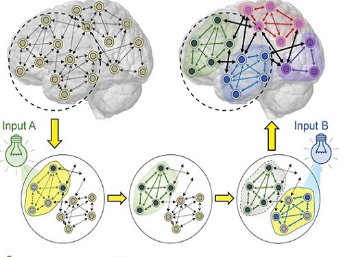
 Before Eyes Open, They Get Ready to See
- Spontaneous retinal waves can generate long-range horizontal connectivity in visual cortex. -
A KAIST research team’s computational simulations demonstrated that the waves of spontaneous neural activity in the retinas of still-closed eyes in mammals develop long-range horizontal connections in the visual cortex during early developmental stages.
This new finding featured in the August 19 edition of Journal of Neuroscience as a cover article has resolved a long-standing puzzle for understanding visual neuroscience regarding the early organization of functional architectures in the mammalian visual cortex before eye-opening, especially the long-range horizontal connectivity known as “feature-specific” circuitry.
To prepare the animal to see when its eyes open, neural circuits in the brain’s visual system must begin developing earlier. However, the proper development of many brain regions involved in vision generally requires sensory input through the eyes.
In the primary visual cortex of the higher mammalian taxa, cortical neurons of similar functional tuning to a visual feature are linked together by long-range horizontal circuits that play a crucial role in visual information processing.
Surprisingly, these long-range horizontal connections in the primary visual cortex of higher mammals emerge before the onset of sensory experience, and the mechanism underlying this phenomenon has remained elusive.
To investigate this mechanism, a group of researchers led by Professor Se-Bum Paik from the Department of Bio and Brain Engineering at KAIST implemented computational simulations of early visual pathways using data obtained from the retinal circuits in young animals before eye-opening, including cats, monkeys, and mice.
From these simulations, the researchers found that spontaneous waves propagating in ON and OFF retinal mosaics can initialize the wiring of long-range horizontal connections by selectively co-activating cortical neurons of similar functional tuning, whereas equivalent random activities cannot induce such organizations.
The simulations also showed that emerged long-range horizontal connections can induce the patterned cortical activities, matching the topography of underlying functional maps even in salt-and-pepper type organizations observed in rodents. This result implies that the model developed by Professor Paik and his group can provide a universal principle for the developmental mechanism of long-range horizontal connections in both higher mammals as well as rodents.
Professor Paik said, “Our model provides a deeper understanding of how the functional architectures in the visual cortex can originate from the spatial organization of the periphery, without sensory experience during early developmental periods.”
He continued, “We believe that our findings will be of great interest to scientists working in a wide range of fields such as neuroscience, vision science, and developmental biology.”
This work was supported by the National Research Foundation of Korea (NRF). Undergraduate student Jinwoo Kim participated in this research project and presented the findings as the lead author as part of the Undergraduate Research Participation (URP) Program at KAIST.
Figures and image credit: Professor Se-Bum Paik, KAIST
Image usage restrictions: News organizations may use or redistribute these figures and image, with proper attribution, as part of news coverage of this paper only.
Publication:
Jinwoo Kim, Min Song, and Se-Bum Paik. (2020). Spontaneous retinal waves generate long-range horizontal connectivity in visual cortex. Journal of Neuroscience, Available online athttps://www.jneurosci.org/content/early/2020/07/17/JNEUROSCI.0649-20.2020
Profile: Se-Bum Paik
Assistant Professor
sbpaik@kaist.ac.kr
http://vs.kaist.ac.kr/
VSNN Laboratory
Department of Bio and Brain Engineering
Program of Brain and Cognitive Engineering
http://kaist.ac.kr
Korea Advanced Institute of Science and Technology (KAIST) Daejeon, Republic of Korea
Profile: Jinwoo Kim
Undergraduate Student
bugkjw@kaist.ac.kr
Department of Bio and Brain Engineering, KAIST
Profile: Min Song
Ph.D. Candidate
night@kaist.ac.kr
Program of Brain and Cognitive Engineering, KAIST
(END)
2020.08.25 View 20124
Before Eyes Open, They Get Ready to See
- Spontaneous retinal waves can generate long-range horizontal connectivity in visual cortex. -
A KAIST research team’s computational simulations demonstrated that the waves of spontaneous neural activity in the retinas of still-closed eyes in mammals develop long-range horizontal connections in the visual cortex during early developmental stages.
This new finding featured in the August 19 edition of Journal of Neuroscience as a cover article has resolved a long-standing puzzle for understanding visual neuroscience regarding the early organization of functional architectures in the mammalian visual cortex before eye-opening, especially the long-range horizontal connectivity known as “feature-specific” circuitry.
To prepare the animal to see when its eyes open, neural circuits in the brain’s visual system must begin developing earlier. However, the proper development of many brain regions involved in vision generally requires sensory input through the eyes.
In the primary visual cortex of the higher mammalian taxa, cortical neurons of similar functional tuning to a visual feature are linked together by long-range horizontal circuits that play a crucial role in visual information processing.
Surprisingly, these long-range horizontal connections in the primary visual cortex of higher mammals emerge before the onset of sensory experience, and the mechanism underlying this phenomenon has remained elusive.
To investigate this mechanism, a group of researchers led by Professor Se-Bum Paik from the Department of Bio and Brain Engineering at KAIST implemented computational simulations of early visual pathways using data obtained from the retinal circuits in young animals before eye-opening, including cats, monkeys, and mice.
From these simulations, the researchers found that spontaneous waves propagating in ON and OFF retinal mosaics can initialize the wiring of long-range horizontal connections by selectively co-activating cortical neurons of similar functional tuning, whereas equivalent random activities cannot induce such organizations.
The simulations also showed that emerged long-range horizontal connections can induce the patterned cortical activities, matching the topography of underlying functional maps even in salt-and-pepper type organizations observed in rodents. This result implies that the model developed by Professor Paik and his group can provide a universal principle for the developmental mechanism of long-range horizontal connections in both higher mammals as well as rodents.
Professor Paik said, “Our model provides a deeper understanding of how the functional architectures in the visual cortex can originate from the spatial organization of the periphery, without sensory experience during early developmental periods.”
He continued, “We believe that our findings will be of great interest to scientists working in a wide range of fields such as neuroscience, vision science, and developmental biology.”
This work was supported by the National Research Foundation of Korea (NRF). Undergraduate student Jinwoo Kim participated in this research project and presented the findings as the lead author as part of the Undergraduate Research Participation (URP) Program at KAIST.
Figures and image credit: Professor Se-Bum Paik, KAIST
Image usage restrictions: News organizations may use or redistribute these figures and image, with proper attribution, as part of news coverage of this paper only.
Publication:
Jinwoo Kim, Min Song, and Se-Bum Paik. (2020). Spontaneous retinal waves generate long-range horizontal connectivity in visual cortex. Journal of Neuroscience, Available online athttps://www.jneurosci.org/content/early/2020/07/17/JNEUROSCI.0649-20.2020
Profile: Se-Bum Paik
Assistant Professor
sbpaik@kaist.ac.kr
http://vs.kaist.ac.kr/
VSNN Laboratory
Department of Bio and Brain Engineering
Program of Brain and Cognitive Engineering
http://kaist.ac.kr
Korea Advanced Institute of Science and Technology (KAIST) Daejeon, Republic of Korea
Profile: Jinwoo Kim
Undergraduate Student
bugkjw@kaist.ac.kr
Department of Bio and Brain Engineering, KAIST
Profile: Min Song
Ph.D. Candidate
night@kaist.ac.kr
Program of Brain and Cognitive Engineering, KAIST
(END)
2020.08.25 View 20124 -
 Novel Via-Hole-Less Multilevel Metal Interconnection Methods
Forming reliable multi-level metal interconnections is a key technology for integrating devices into organic integrated circuits (ICs). The conventional approach, called “via-hole,” locally removes the insulator and utilizes metal interconnects through the holes. Due to the high sensitivity of organic materials to chemical solvents, heat, and photo-radiation used in conventional “via-hole” methods, alternative printing methods or laser drilling methods have been developed. However, finding a reliable and practical metal interconnection for organic ICs is still challenging.
The research team of KAIST Professor Sung Gap Im and Postech Professor Kim Jae-Joon reported a new interconnection method that does not require via-hole formation, “via-hole-less metal interconnection,” in Nature Communications on June 3.
Metal electrodes in different layers can be isolated from each other by patterned dielectric layers, where they then can be interconnected to others in the open area where the dielectric layer is not present. See the images below. Vapor phase deposition and in-situ patterning of dielectric layer using iCVD (initiated chemical vapor deposition), used in the “via-hole-less” method, ensure a damage-free process for organic semiconductor materials and result in outstanding performance of the organic devices as multilevel metal interconnects are reliably formed. The team successfully demonstrated three-dimensional (3D) stacking of five organic transistors and integrated circuits using the proposed via-hole-less interconnect method. See the image below.
Vapor phase deposition and in-situ patterning of dielectric layer using iCVD (initiated chemical vapor deposition), used in the “via-hole-less” method, ensure a damage-free process for organic semiconductor materials and result in outstanding performance of the organic devices as multilevel metal interconnects are reliably formed. The team successfully demonstrated three-dimensional (3D) stacking of five organic transistors and integrated circuits using the proposed via-hole-less interconnect method. See the image below.
Professor Kim explained, “Our proposed via-hole-less interconnect method using a selectively patterned dielectric overcomes the limitations of the previous time-consuming, one-by-one via-hole formation process and provides reliable methods for creating metal interconnects in organic ICs. We expect the via-hole-less scheme to bring advances to organic IC technology.”
2019.06.18 View 49594
Novel Via-Hole-Less Multilevel Metal Interconnection Methods
Forming reliable multi-level metal interconnections is a key technology for integrating devices into organic integrated circuits (ICs). The conventional approach, called “via-hole,” locally removes the insulator and utilizes metal interconnects through the holes. Due to the high sensitivity of organic materials to chemical solvents, heat, and photo-radiation used in conventional “via-hole” methods, alternative printing methods or laser drilling methods have been developed. However, finding a reliable and practical metal interconnection for organic ICs is still challenging.
The research team of KAIST Professor Sung Gap Im and Postech Professor Kim Jae-Joon reported a new interconnection method that does not require via-hole formation, “via-hole-less metal interconnection,” in Nature Communications on June 3.
Metal electrodes in different layers can be isolated from each other by patterned dielectric layers, where they then can be interconnected to others in the open area where the dielectric layer is not present. See the images below. Vapor phase deposition and in-situ patterning of dielectric layer using iCVD (initiated chemical vapor deposition), used in the “via-hole-less” method, ensure a damage-free process for organic semiconductor materials and result in outstanding performance of the organic devices as multilevel metal interconnects are reliably formed. The team successfully demonstrated three-dimensional (3D) stacking of five organic transistors and integrated circuits using the proposed via-hole-less interconnect method. See the image below.
Vapor phase deposition and in-situ patterning of dielectric layer using iCVD (initiated chemical vapor deposition), used in the “via-hole-less” method, ensure a damage-free process for organic semiconductor materials and result in outstanding performance of the organic devices as multilevel metal interconnects are reliably formed. The team successfully demonstrated three-dimensional (3D) stacking of five organic transistors and integrated circuits using the proposed via-hole-less interconnect method. See the image below.
Professor Kim explained, “Our proposed via-hole-less interconnect method using a selectively patterned dielectric overcomes the limitations of the previous time-consuming, one-by-one via-hole formation process and provides reliable methods for creating metal interconnects in organic ICs. We expect the via-hole-less scheme to bring advances to organic IC technology.”
2019.06.18 View 49594 -
 First Female Grand Prize Awardee of Samsung Humantech
Yeunhee Huh, PhD candidate (Professor Gyu-Hyeong Cho) from the School of Electrical Engineering received the grand prize of the 24th Humantech Paper Award. She is the first female recipient of this prize since its establishment in 1994. The Humantech Paper Award is hosted by Samsung Electronics and sponsored by the Ministry of Science and ICT with JoongAng Daily Newspaper. Her paper is titled, ‘A Hybrid Structure Dual-Path Step-Down Converter with 96.2% Peak Efficiency using 250mΩ Large-DCR Inductor’. Electronic devices require numerous chips and have a power converter to supply energy adequately. She proposed a new structure to enhance energy efficiency by combining inductors and capacitors. Enhancing energy efficiency can reduce energy loss, which prolongs battery hours and solves overheating of devices; for instance, energy loss leads to the overheating issue affecting phone chargers. This technology can be applied to various electronic devices, such as cell phones, laptops, and drones. Huh said, “Power has to go up in order to meet customers’ needs; however the overheating problem emerges during this process. This problem affects surrounding circuits and causes other issues, such as malfunctions of electronic devices. This technology may vary according to the conditions, but it can enhance energy efficiency up to 4%.”During the ceremony, about eight hundred million KRW worth cash prizes was conferred to 119 papers. KAIST (44 papers) and Gyeonggi Science High School (6 papers) received special awards given to the schools.
2018.02.12 View 14822
First Female Grand Prize Awardee of Samsung Humantech
Yeunhee Huh, PhD candidate (Professor Gyu-Hyeong Cho) from the School of Electrical Engineering received the grand prize of the 24th Humantech Paper Award. She is the first female recipient of this prize since its establishment in 1994. The Humantech Paper Award is hosted by Samsung Electronics and sponsored by the Ministry of Science and ICT with JoongAng Daily Newspaper. Her paper is titled, ‘A Hybrid Structure Dual-Path Step-Down Converter with 96.2% Peak Efficiency using 250mΩ Large-DCR Inductor’. Electronic devices require numerous chips and have a power converter to supply energy adequately. She proposed a new structure to enhance energy efficiency by combining inductors and capacitors. Enhancing energy efficiency can reduce energy loss, which prolongs battery hours and solves overheating of devices; for instance, energy loss leads to the overheating issue affecting phone chargers. This technology can be applied to various electronic devices, such as cell phones, laptops, and drones. Huh said, “Power has to go up in order to meet customers’ needs; however the overheating problem emerges during this process. This problem affects surrounding circuits and causes other issues, such as malfunctions of electronic devices. This technology may vary according to the conditions, but it can enhance energy efficiency up to 4%.”During the ceremony, about eight hundred million KRW worth cash prizes was conferred to 119 papers. KAIST (44 papers) and Gyeonggi Science High School (6 papers) received special awards given to the schools.
2018.02.12 View 14822 -
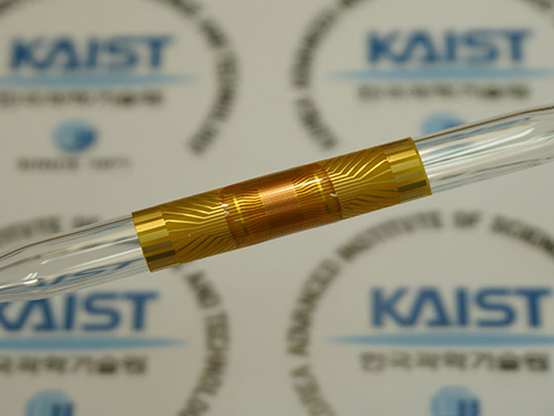 Continuous Roll-Process Technology for Transferring and Packaging Flexible Large-Scale Integrated Circuits
A research team led by Professor Keon Jae Lee from KAIST and by Dr. Jae-Hyun Kim from the Korea Institute of Machinery and Materials (KIMM) has jointly developed a continuous roll-processing technology that transfers and packages flexible large-scale integrated circuits (LSI), the key element in constructing the computer’s brain such as CPU, on plastics to realize flexible electronics.
Professor Lee previously demonstrated the silicon-based flexible LSIs using 0.18 CMOS (complementary metal-oxide semiconductor) process in 2013 (ACS Nano, “In Vivo Silicon-based Flexible Radio Frequency Integrated Circuits Monolithically Encapsulated with Biocompatible Liquid Crystal Polymers”) and presented the work in an invited talk of 2015 International Electron Device Meeting (IEDM), the world’s premier semiconductor forum.
Highly productive roll-processing is considered a core technology for accelerating the commercialization of wearable computers using flexible LSI. However, realizing it has been a difficult challenge not only from the roll-based manufacturing perspective but also for creating roll-based packaging for the interconnection of flexible LSI with flexible displays, batteries, and other peripheral devices.
To overcome these challenges, the research team started fabricating NAND flash memories on a silicon wafer using conventional semiconductor processes, and then removed a sacrificial wafer leaving a top hundreds-nanometer-thick circuit layer. Next, they simultaneously transferred and interconnected the ultrathin device on a flexible substrate through the continuous roll-packaging technology using anisotropic conductive film (ACF). The final silicon-based flexible NAND memory successfully demonstrated stable memory operations and interconnections even under severe bending conditions. This roll-based flexible LSI technology can be potentially utilized to produce flexible application processors (AP), high-density memories, and high-speed communication devices for mass manufacture.
Professor Lee said, “Highly productive roll-process was successfully applied to flexible LSIs to continuously transfer and interconnect them onto plastics. For example, we have confirmed the reliable operation of our flexible NAND memory at the circuit level by programming and reading letters in ASCII codes. Out results may open up new opportunities to integrate silicon-based flexible LSIs on plastics with the ACF packing for roll-based manufacturing.”
Dr. Kim added, “We employed the roll-to-plate ACF packaging, which showed outstanding bonding capability for continuous roll-based transfer and excellent flexibility of interconnecting core and peripheral devices. This can be a key process to the new era of flexible computers combining the already developed flexible displays and batteries.”
The team’s results will be published on the front cover of Advanced Materials (August 31, 2016) in an article entitled “Simultaneous Roll Transfer and Interconnection of Silicon NAND Flash Memory.” (DOI: 10.1002/adma.201602339)
YouTube Link: https://www.youtube.com/watch?v=8OJjAEm27sw
Picture 1: This schematic image shows the flexible silicon NAND flash memory produced by the simultaneous roll-transfer and interconnection process.
Picture 2: The flexible silicon NAND flash memory is attached to a 7 mm diameter glass rod.
2016.09.01 View 15894
Continuous Roll-Process Technology for Transferring and Packaging Flexible Large-Scale Integrated Circuits
A research team led by Professor Keon Jae Lee from KAIST and by Dr. Jae-Hyun Kim from the Korea Institute of Machinery and Materials (KIMM) has jointly developed a continuous roll-processing technology that transfers and packages flexible large-scale integrated circuits (LSI), the key element in constructing the computer’s brain such as CPU, on plastics to realize flexible electronics.
Professor Lee previously demonstrated the silicon-based flexible LSIs using 0.18 CMOS (complementary metal-oxide semiconductor) process in 2013 (ACS Nano, “In Vivo Silicon-based Flexible Radio Frequency Integrated Circuits Monolithically Encapsulated with Biocompatible Liquid Crystal Polymers”) and presented the work in an invited talk of 2015 International Electron Device Meeting (IEDM), the world’s premier semiconductor forum.
Highly productive roll-processing is considered a core technology for accelerating the commercialization of wearable computers using flexible LSI. However, realizing it has been a difficult challenge not only from the roll-based manufacturing perspective but also for creating roll-based packaging for the interconnection of flexible LSI with flexible displays, batteries, and other peripheral devices.
To overcome these challenges, the research team started fabricating NAND flash memories on a silicon wafer using conventional semiconductor processes, and then removed a sacrificial wafer leaving a top hundreds-nanometer-thick circuit layer. Next, they simultaneously transferred and interconnected the ultrathin device on a flexible substrate through the continuous roll-packaging technology using anisotropic conductive film (ACF). The final silicon-based flexible NAND memory successfully demonstrated stable memory operations and interconnections even under severe bending conditions. This roll-based flexible LSI technology can be potentially utilized to produce flexible application processors (AP), high-density memories, and high-speed communication devices for mass manufacture.
Professor Lee said, “Highly productive roll-process was successfully applied to flexible LSIs to continuously transfer and interconnect them onto plastics. For example, we have confirmed the reliable operation of our flexible NAND memory at the circuit level by programming and reading letters in ASCII codes. Out results may open up new opportunities to integrate silicon-based flexible LSIs on plastics with the ACF packing for roll-based manufacturing.”
Dr. Kim added, “We employed the roll-to-plate ACF packaging, which showed outstanding bonding capability for continuous roll-based transfer and excellent flexibility of interconnecting core and peripheral devices. This can be a key process to the new era of flexible computers combining the already developed flexible displays and batteries.”
The team’s results will be published on the front cover of Advanced Materials (August 31, 2016) in an article entitled “Simultaneous Roll Transfer and Interconnection of Silicon NAND Flash Memory.” (DOI: 10.1002/adma.201602339)
YouTube Link: https://www.youtube.com/watch?v=8OJjAEm27sw
Picture 1: This schematic image shows the flexible silicon NAND flash memory produced by the simultaneous roll-transfer and interconnection process.
Picture 2: The flexible silicon NAND flash memory is attached to a 7 mm diameter glass rod.
2016.09.01 View 15894