electron
-
 Approaches to Human-Robot Interaction Using Biosignals
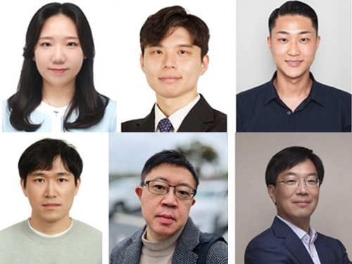
<(From left) Dr. Hwa-young Jeong, Professor Kyung-seo Park, Dr. Yoon-tae Jeong, Dr. Ji-hoon Seo, Professor Min-kyu Je, Professor Jung Kim >
A joint research team led by Professor Jung Kim of KAIST Department of Mechanical Engineering and Professor Min-kyu Je of the Department of Electrical and Electronic Engineering recently published a review paper on the latest trends and advancements in intuitive Human-Robot Interaction (HRI) using bio-potential and bio-impedance in the internationally renowned academic journal 'Nature Reviews Electrical Engineering'.
This review paper is the result of a collaborative effort by Dr. Kyung-seo Park (DGIST, co-first author), Dr. Hwa-young Jeong (EPFL, co-first author), Dr. Yoon-tae Jeong (IMEC), and Dr. Ji-hoon Seo (UCSD), all doctoral graduates from the two laboratories. Nature Reviews Electrical Engineering is a review specialized journal in the field of electrical, electronic, and artificial intelligence technology, newly launched by Nature Publishing Group last year. It is known to invite world-renowned scholars in the field through strict selection criteria. Professor Jung Kim's research team's paper, titled "Using bio-potential and bio-impedance for intuitive human-robot interaction," was published on July 18, 2025. (DOI: https://doi.org/10.1038/s44287-025-00191-5)
This review paper explains how biosignals can be used to quickly and accurately detect movement intentions and introduces advancements in movement prediction technology based on neural signals and muscle activity. It also focuses on the crucial role of integrated circuits (ICs) in maximizing low-noise performance and energy efficiency in biosignal sensing, covering thelatest development trends in low-noise, low-power designs for accurately measuring bio-potential and impedance signals.
The review emphasizes the importance of hybrid and multi-modal sensing approaches, presenting the possibility of building robust, intuitive, and scalable HRI systems. The research team stressed that collaboration between sensor and IC design fields is essential for the practical application of biosignal-based HRI systems and stated that interdisciplinary collaboration will play a significant role in the development of next-generation HRI technology. Dr. Hwa-young Jeong, a co-first author of the paper, presented the potential of bio-potential and impedance signals to make human-robot interaction more intuitive and efficient, predicting that it will make significant contributions to the development of HRI technologies such as rehabilitation robots and robotic prostheses using biosignals in the future. This research was supported by several research projects, including the Human Plus Project of the National Research Foundation of Korea.
2025.07.24 View 343
Approaches to Human-Robot Interaction Using Biosignals
<(From left) Dr. Hwa-young Jeong, Professor Kyung-seo Park, Dr. Yoon-tae Jeong, Dr. Ji-hoon Seo, Professor Min-kyu Je, Professor Jung Kim >
A joint research team led by Professor Jung Kim of KAIST Department of Mechanical Engineering and Professor Min-kyu Je of the Department of Electrical and Electronic Engineering recently published a review paper on the latest trends and advancements in intuitive Human-Robot Interaction (HRI) using bio-potential and bio-impedance in the internationally renowned academic journal 'Nature Reviews Electrical Engineering'.
This review paper is the result of a collaborative effort by Dr. Kyung-seo Park (DGIST, co-first author), Dr. Hwa-young Jeong (EPFL, co-first author), Dr. Yoon-tae Jeong (IMEC), and Dr. Ji-hoon Seo (UCSD), all doctoral graduates from the two laboratories. Nature Reviews Electrical Engineering is a review specialized journal in the field of electrical, electronic, and artificial intelligence technology, newly launched by Nature Publishing Group last year. It is known to invite world-renowned scholars in the field through strict selection criteria. Professor Jung Kim's research team's paper, titled "Using bio-potential and bio-impedance for intuitive human-robot interaction," was published on July 18, 2025. (DOI: https://doi.org/10.1038/s44287-025-00191-5)
This review paper explains how biosignals can be used to quickly and accurately detect movement intentions and introduces advancements in movement prediction technology based on neural signals and muscle activity. It also focuses on the crucial role of integrated circuits (ICs) in maximizing low-noise performance and energy efficiency in biosignal sensing, covering thelatest development trends in low-noise, low-power designs for accurately measuring bio-potential and impedance signals.
The review emphasizes the importance of hybrid and multi-modal sensing approaches, presenting the possibility of building robust, intuitive, and scalable HRI systems. The research team stressed that collaboration between sensor and IC design fields is essential for the practical application of biosignal-based HRI systems and stated that interdisciplinary collaboration will play a significant role in the development of next-generation HRI technology. Dr. Hwa-young Jeong, a co-first author of the paper, presented the potential of bio-potential and impedance signals to make human-robot interaction more intuitive and efficient, predicting that it will make significant contributions to the development of HRI technologies such as rehabilitation robots and robotic prostheses using biosignals in the future. This research was supported by several research projects, including the Human Plus Project of the National Research Foundation of Korea.
2025.07.24 View 343 -
 Professor Jung-woo' Choi ‘s Team Comes in First at the World's Top Acoustic AI Challenge
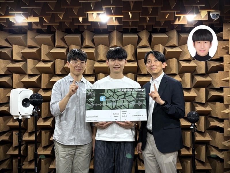
<Photo1. (From left) Ph.D candidate Yong-hoo Kwon, M.S candidate Do-hwan Kim, Professor Jung-woo Choi, Dr. Dong-heon Lee>
'Acoustic separation and classification technology' is a next-generation artificial intelligence (AI) core technology that enables the early detection of abnormal sounds in areas such as drones, fault detection of factory pipelines, and border surveillance systems, or allows for the separation and editing of spatial audio by sound source when producing AR/VR content.
On the 11th of July, a research team led by Professor Jung-woo Choi of KAIST's Department of Electrical and Electronic Engineering won first place in the 'Spatial Semantic Segmentation of Sound Scenes' task of the 'DCASE2025 Challenge,' the world's most prestigious acoustic detection and analysis competition.
This year’s challenge featured 86 teams competing across six tasks. In this competition, the KAIST research team achieved the best performance in their first-ever participation to Task 4. Professor Jung-woo Choi’s research team consisted of Dr. Dong-heon, Lee, Ph.D. candidate Young-hoo Kwon, and M.S. candidate Do-hwan Kim.
Task 4 titled 'Spatial Semantic Segmentation of Sound Scenes' is a highly demanding task requiring the analysis of spatial information in multi-channel audio signals with overlapping sound sources. The goal was to separate individual sounds and classify them into 18 predefined categories. The research team plans to present their technology at the DCASE workshop in Barcelona this October.
<Figure 1. Example of an acoustic scene with multiple mixed sounds>
Early this year, Dr. Dong-heon Lee developed a state-of-the-art sound source separation AI that combines Transformer and Mamba architectures. During the competition, centered around researcher Young-hoo Kwon, they completed a ‘chain-of-inference architecture' AI model that performs sound source separation and classification again, using the waveforms and types of the initially separated sound sources as clues. This AI model is inspired by human’s auditory scene analysis mechanism that isolates individual sounds by focusing on incomplete clues such as sound type, rhythm, or direction, when listening to complex sounds.
Through this, the team was the only participant to achieve double-digit performance (11 dB) in 'Class-Aware Signal-to-Distortion Ratio Improvement (CA-SDRi)*,' which is the measure for ranking how well the AI separated and classified sounds, proving their technical excellence.
Class-Aware Signal-to-Distortion Ratio Improvement (CA-SDRi): Measures how much clearer (less distorted) the desired sound is separated and classified compared to the original audio, in dB (decibels). A higher number indicates more accurate and cleaner sound separation.
Prof. Jung-woo Choi remarked, "The research team has showcased world-leading acoustic separation AI models for the past three years, and I am delighted that these results have been officially recognized." He added, "I am proud of every member of the research team for winning first place through focused research, despite the significant increase in difficulty and having only a few weeks for development."
<Figure 2. Time-frequency patterns of sound sources separated from a mixed source>
The IEEE DCASE Challenge 2025 was held online, with submissions accepted from April 1 to June 15 and results announced on June 30. Since its launch in 2013, the DCASE Challenge has served as a premier global platform of IEEE Signal Processing Society for showcasing cutting-edge AI models in acoustic signal processing.
This research was supported by the Mid-Career Researcher Support Project and STEAM Research Project of the National Research Foundation of Korea, funded by the Ministry of Education, Science and Technology, as well as support from the Future Defense Research Center, funded by the Defense Acquisition Program Administration and the Agency for Defense Development.
2025.07.13 View 399
Professor Jung-woo' Choi ‘s Team Comes in First at the World's Top Acoustic AI Challenge
<Photo1. (From left) Ph.D candidate Yong-hoo Kwon, M.S candidate Do-hwan Kim, Professor Jung-woo Choi, Dr. Dong-heon Lee>
'Acoustic separation and classification technology' is a next-generation artificial intelligence (AI) core technology that enables the early detection of abnormal sounds in areas such as drones, fault detection of factory pipelines, and border surveillance systems, or allows for the separation and editing of spatial audio by sound source when producing AR/VR content.
On the 11th of July, a research team led by Professor Jung-woo Choi of KAIST's Department of Electrical and Electronic Engineering won first place in the 'Spatial Semantic Segmentation of Sound Scenes' task of the 'DCASE2025 Challenge,' the world's most prestigious acoustic detection and analysis competition.
This year’s challenge featured 86 teams competing across six tasks. In this competition, the KAIST research team achieved the best performance in their first-ever participation to Task 4. Professor Jung-woo Choi’s research team consisted of Dr. Dong-heon, Lee, Ph.D. candidate Young-hoo Kwon, and M.S. candidate Do-hwan Kim.
Task 4 titled 'Spatial Semantic Segmentation of Sound Scenes' is a highly demanding task requiring the analysis of spatial information in multi-channel audio signals with overlapping sound sources. The goal was to separate individual sounds and classify them into 18 predefined categories. The research team plans to present their technology at the DCASE workshop in Barcelona this October.
<Figure 1. Example of an acoustic scene with multiple mixed sounds>
Early this year, Dr. Dong-heon Lee developed a state-of-the-art sound source separation AI that combines Transformer and Mamba architectures. During the competition, centered around researcher Young-hoo Kwon, they completed a ‘chain-of-inference architecture' AI model that performs sound source separation and classification again, using the waveforms and types of the initially separated sound sources as clues. This AI model is inspired by human’s auditory scene analysis mechanism that isolates individual sounds by focusing on incomplete clues such as sound type, rhythm, or direction, when listening to complex sounds.
Through this, the team was the only participant to achieve double-digit performance (11 dB) in 'Class-Aware Signal-to-Distortion Ratio Improvement (CA-SDRi)*,' which is the measure for ranking how well the AI separated and classified sounds, proving their technical excellence.
Class-Aware Signal-to-Distortion Ratio Improvement (CA-SDRi): Measures how much clearer (less distorted) the desired sound is separated and classified compared to the original audio, in dB (decibels). A higher number indicates more accurate and cleaner sound separation.
Prof. Jung-woo Choi remarked, "The research team has showcased world-leading acoustic separation AI models for the past three years, and I am delighted that these results have been officially recognized." He added, "I am proud of every member of the research team for winning first place through focused research, despite the significant increase in difficulty and having only a few weeks for development."
<Figure 2. Time-frequency patterns of sound sources separated from a mixed source>
The IEEE DCASE Challenge 2025 was held online, with submissions accepted from April 1 to June 15 and results announced on June 30. Since its launch in 2013, the DCASE Challenge has served as a premier global platform of IEEE Signal Processing Society for showcasing cutting-edge AI models in acoustic signal processing.
This research was supported by the Mid-Career Researcher Support Project and STEAM Research Project of the National Research Foundation of Korea, funded by the Ministry of Education, Science and Technology, as well as support from the Future Defense Research Center, funded by the Defense Acquisition Program Administration and the Agency for Defense Development.
2025.07.13 View 399 -
 Military Combatants Usher in an Era of Personalized Training with New Materials
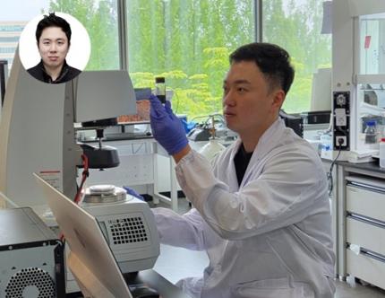
< Photo 1. (From left) Professor Steve Park of Materials Science and Engineering, Kyusoon Pak, Ph.D. Candidate (Army Major) >
Traditional military training often relies on standardized methods, which has limited the provision of optimized training tailored to individual combatants' characteristics or specific combat situations. To address this, our research team developed an e-textile platform, securing core technology that can reflect the unique traits of individual combatants and various combat scenarios. This technology has proven robust enough for battlefield use and is economical enough for widespread distribution to a large number of troops.
On June 25th, Professor Steve Park's research team at KAIST's Department of Materials Science and Engineering announced the development of a flexible, wearable electronic textile (E-textile) platform using an innovative technology that 'draws' electronic circuits directly onto fabric.
The wearable e-textile platform developed by the research team combines 3D printing technology with new materials engineering design to directly print flexible and highly durable sensors and electrodes onto textile substrates. This enables the collection of precise movement and human body data from individual combatants, which can then be used to propose customized training models.
Existing e-textile fabrication methods were often complex or limited in their ability to provide personalized customization. To overcome these challenges, the research team adopted an additive manufacturing technology called 'Direct Ink Writing (DIW)' 3D printing.
< Figure 1. Schematic diagram of e-textile manufactured with Direct Ink Writing (DIW) printing technology on various textiles, including combat uniforms >
This technology involves directly dispensing and printing special ink, which functions as sensors and electrodes, onto textile substrates in desired patterns. This allows for flexible implementation of various designs without the complex process of mask fabrication. This is expected to be an effective technology that can be easily supplied to hundreds of thousands of military personnel.
The core of this technology lies in the development of high-performance functional inks based on advanced materials engineering design. The research team combined styrene-butadiene-styrene (SBS) polymer, which provides flexibility, with multi-walled carbon nanotubes (MWCNT) for electrical conductivity. They developed a tensile/bending sensor ink that can stretch up to 102% and maintain stable performance even after 10,000 repetitive tests. This means that accurate data can be consistently obtained even during the strenuous movements of combatants.
< Figure 2. Measurement of human movement and breathing patterns using e-textile >
Furthermore, new material technology was applied to implement 'interconnect electrodes' that electrically connect the upper and lower layers of the fabric. The team developed an electrode ink combining silver (Ag) flakes with rigid polystyrene (PS) polymer, precisely controlling the impregnation level (how much the ink penetrates the fabric) to effectively connect both sides or multiple layers of the fabric. This secures the technology for producing multi-layered wearable electronic systems integrating sensors and electrodes.
< Figure 3. Experimental results of recognizing unknown objects after machine learning six objects using a smart glove >
The research team proved the platform's performance through actual human movement monitoring experiments. They printed the developed e-textile on major joint areas of clothing (shoulders, elbows, knees) and measured movements and posture changes during various exercises such as running, jumping jacks, and push-ups in real-time.
Additionally, they demonstrated the potential for applications such as monitoring breathing patterns using a smart mask and recognizing objects through machine learning and perceiving complex tactile information by printing multiple sensors and electrodes on gloves. These results show that the developed e-textile platform is effective in precisely understanding the movement dynamics of combatants.
This research is an important example demonstrating how cutting-edge new material technology can contribute to the advancement of the defense sector. Major Kyusoon Pak of the Army, who participated in this research, considered required objectives such as military applicability and economic feasibility for practical distribution from the research design stage.
< Figure 4. Experimental results showing that a multi-layered e-textile glove connected with interconnect electrodes can measure tensile/bending signals and pressure signals at a single point >
Major Pak stated, "Our military is currently facing both a crisis and an opportunity due to the decrease in military personnel resources caused by the demographic cliff and the advancement of science and technology. Also, respect for life in the battlefield is emerging as a significant issue. This research aims to secure original technology that can provide customized training according to military branch/duty and type of combat, thereby enhancing the combat power and ensuring the survivability of our soldiers."
He added, "I hope this research will be evaluated as a case that achieved both scientific contribution and military applicability."
This research, where Kyusoon Pak, Ph.D. Candidate (Army Major) from KAIST's Department of Materials Science and Engineering, participated as the first author and Professor Steve Park supervised, was published on May 27, 2025, in `npj Flexible Electronics (top 1.8% in JCR field)', an international academic journal in the electrical, electronic, and materials engineering fields.
* Paper Title: Fabrication of Multifunctional Wearable Interconnect E-textile Platform Using Direct Ink Writing (DIW) 3D Printing
* DOI: https://doi.org/10.1038/s41528-025-00414-7
This research was supported by the Ministry of Trade, Industry and Energy and the National Research Foundation of Korea.
2025.06.25 View 1867
Military Combatants Usher in an Era of Personalized Training with New Materials
< Photo 1. (From left) Professor Steve Park of Materials Science and Engineering, Kyusoon Pak, Ph.D. Candidate (Army Major) >
Traditional military training often relies on standardized methods, which has limited the provision of optimized training tailored to individual combatants' characteristics or specific combat situations. To address this, our research team developed an e-textile platform, securing core technology that can reflect the unique traits of individual combatants and various combat scenarios. This technology has proven robust enough for battlefield use and is economical enough for widespread distribution to a large number of troops.
On June 25th, Professor Steve Park's research team at KAIST's Department of Materials Science and Engineering announced the development of a flexible, wearable electronic textile (E-textile) platform using an innovative technology that 'draws' electronic circuits directly onto fabric.
The wearable e-textile platform developed by the research team combines 3D printing technology with new materials engineering design to directly print flexible and highly durable sensors and electrodes onto textile substrates. This enables the collection of precise movement and human body data from individual combatants, which can then be used to propose customized training models.
Existing e-textile fabrication methods were often complex or limited in their ability to provide personalized customization. To overcome these challenges, the research team adopted an additive manufacturing technology called 'Direct Ink Writing (DIW)' 3D printing.
< Figure 1. Schematic diagram of e-textile manufactured with Direct Ink Writing (DIW) printing technology on various textiles, including combat uniforms >
This technology involves directly dispensing and printing special ink, which functions as sensors and electrodes, onto textile substrates in desired patterns. This allows for flexible implementation of various designs without the complex process of mask fabrication. This is expected to be an effective technology that can be easily supplied to hundreds of thousands of military personnel.
The core of this technology lies in the development of high-performance functional inks based on advanced materials engineering design. The research team combined styrene-butadiene-styrene (SBS) polymer, which provides flexibility, with multi-walled carbon nanotubes (MWCNT) for electrical conductivity. They developed a tensile/bending sensor ink that can stretch up to 102% and maintain stable performance even after 10,000 repetitive tests. This means that accurate data can be consistently obtained even during the strenuous movements of combatants.
< Figure 2. Measurement of human movement and breathing patterns using e-textile >
Furthermore, new material technology was applied to implement 'interconnect electrodes' that electrically connect the upper and lower layers of the fabric. The team developed an electrode ink combining silver (Ag) flakes with rigid polystyrene (PS) polymer, precisely controlling the impregnation level (how much the ink penetrates the fabric) to effectively connect both sides or multiple layers of the fabric. This secures the technology for producing multi-layered wearable electronic systems integrating sensors and electrodes.
< Figure 3. Experimental results of recognizing unknown objects after machine learning six objects using a smart glove >
The research team proved the platform's performance through actual human movement monitoring experiments. They printed the developed e-textile on major joint areas of clothing (shoulders, elbows, knees) and measured movements and posture changes during various exercises such as running, jumping jacks, and push-ups in real-time.
Additionally, they demonstrated the potential for applications such as monitoring breathing patterns using a smart mask and recognizing objects through machine learning and perceiving complex tactile information by printing multiple sensors and electrodes on gloves. These results show that the developed e-textile platform is effective in precisely understanding the movement dynamics of combatants.
This research is an important example demonstrating how cutting-edge new material technology can contribute to the advancement of the defense sector. Major Kyusoon Pak of the Army, who participated in this research, considered required objectives such as military applicability and economic feasibility for practical distribution from the research design stage.
< Figure 4. Experimental results showing that a multi-layered e-textile glove connected with interconnect electrodes can measure tensile/bending signals and pressure signals at a single point >
Major Pak stated, "Our military is currently facing both a crisis and an opportunity due to the decrease in military personnel resources caused by the demographic cliff and the advancement of science and technology. Also, respect for life in the battlefield is emerging as a significant issue. This research aims to secure original technology that can provide customized training according to military branch/duty and type of combat, thereby enhancing the combat power and ensuring the survivability of our soldiers."
He added, "I hope this research will be evaluated as a case that achieved both scientific contribution and military applicability."
This research, where Kyusoon Pak, Ph.D. Candidate (Army Major) from KAIST's Department of Materials Science and Engineering, participated as the first author and Professor Steve Park supervised, was published on May 27, 2025, in `npj Flexible Electronics (top 1.8% in JCR field)', an international academic journal in the electrical, electronic, and materials engineering fields.
* Paper Title: Fabrication of Multifunctional Wearable Interconnect E-textile Platform Using Direct Ink Writing (DIW) 3D Printing
* DOI: https://doi.org/10.1038/s41528-025-00414-7
This research was supported by the Ministry of Trade, Industry and Energy and the National Research Foundation of Korea.
2025.06.25 View 1867 -
 KAIST Successfully Develops High-Performance Water Electrolysis Without Platinum, Bringing Hydrogen Economy Closer
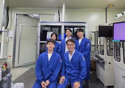
< Photo 1. (Front row, from left) Jeesoo Park (Ph.D. Candidate), Professor Hee-Tak Kim (Back row, from left) Kyunghwa Seok (Ph.D. Candidate), Dr. Gisu Doo, Euntaek Oh (Ph.D. Candidate) >
Hydrogen is gaining attention as a clean energy source that emits no carbon. Among various methods, water electrolysis, which splits water into hydrogen and oxygen using electricity, is recognized as an eco-friendly hydrogen production method. Specifically, proton exchange membrane water electrolysis (PEMWE) is considered a next-generation hydrogen production technology due to its ability to produce high-purity hydrogen at high pressure. However, existing PEMWE technology has faced limitations in commercialization due to its heavy reliance on expensive precious metal catalysts and coating materials. Korean researchers have now proposed a new solution to address these technical and economic bottlenecks.
KAIST (President Kwang Hyung Lee) announced on June 11th that a research team led by Professor Hee-Tak Kim of the Department of Chemical and Biomolecular Engineering, in a joint study with Dr. Gisu Doo of the Korea Institute of Energy Research (KIER, President Chang-keun Lee), has developed a next-generation water electrolysis technology that achieves high performance without the need for expensive platinum (Pt) coating.
The research team focused on the primary reason why 'iridium oxide (IrOx),' a highly active catalyst for water electrolysis electrodes, fails to perform optimally. They found that this is due to inefficient electron transfer and, for the first time in the world, demonstrated that performance can be maximized simply by controlling the catalyst particle size.
In this study, it was revealed that the reason iridium oxide catalysts do not exhibit excellent performance without platinum coating is due to 'electron transport resistance' that occurs at the interface between the catalyst, the ion conductor (hereinafter referred to as ionomer), and the Ti (titanium) substrate—core components inherently used together in water electrolysis electrodes.
Specifically, they identified that the 'pinch-off' phenomenon, where the electron pathway is blocked between the catalyst, ionomer, and titanium substrate, is the critical cause of reduced conductivity. The ionomer has properties close to an electron insulator, thereby hindering electron flow when it surrounds catalyst particles. Furthermore, when the ionomer comes into contact with the titanium substrate, an electron barrier forms on the surface oxide layer of the titanium substrate, significantly increasing resistance.
< Figure 1. Infographic related to electron transport resistance at the catalyst layer/diffusion layer interface >
To address this, the research team fabricated and compared catalysts of various particle sizes. Through single-cell evaluation and multiphysics simulations, they demonstrated, for the first time globally, that when iridium oxide catalyst particles with a size of 20 nanometers (nm) or larger are used, the ionomer mixed region decreases, ensuring an electron pathway and restoring conductivity.
Moreover, they successfully optimized the interfacial structure through precise design, simultaneously ensuring both reactivity and electron transport. This achievement demonstrated that the previously unavoidable trade-off between catalyst activity and conductivity can be overcome through meticulous interfacial design.
This breakthrough is expected to be a significant milestone not only for the development of high-performance catalyst materials but also for the future commercialization of proton exchange membrane water electrolysis systems that can achieve high efficiency while drastically reducing the amount of precious metals used.
Professor Hee-Tak Kim stated, "This research presents a new interface design strategy that can resolve the interfacial conductivity problem, which was a bottleneck in high-performance water electrolysis technology." He added, "By securing high performance even without expensive materials like platinum, it will be a stepping stone closer to realizing a hydrogen economy."
This research, with Jeesoo Park, a Ph.D. student from the Department of Chemical and Biomolecular Engineering at KAIST, as the first author, was published on June 7th in 'Energy & Environmental Science' (IF: 32.4, 2025), a leading international journal in the energy and environmental fields, and was recognized for its innovativeness and impact. (Paper title: On the interface electron transport problem of highly active IrOx catalysts, DOI: 10.1039/D4EE05816J).
This research was supported by the New and Renewable Energy Core Technology Development Project of the Ministry of Trade, Industry and Energy.
2025.06.11 View 3286
KAIST Successfully Develops High-Performance Water Electrolysis Without Platinum, Bringing Hydrogen Economy Closer
< Photo 1. (Front row, from left) Jeesoo Park (Ph.D. Candidate), Professor Hee-Tak Kim (Back row, from left) Kyunghwa Seok (Ph.D. Candidate), Dr. Gisu Doo, Euntaek Oh (Ph.D. Candidate) >
Hydrogen is gaining attention as a clean energy source that emits no carbon. Among various methods, water electrolysis, which splits water into hydrogen and oxygen using electricity, is recognized as an eco-friendly hydrogen production method. Specifically, proton exchange membrane water electrolysis (PEMWE) is considered a next-generation hydrogen production technology due to its ability to produce high-purity hydrogen at high pressure. However, existing PEMWE technology has faced limitations in commercialization due to its heavy reliance on expensive precious metal catalysts and coating materials. Korean researchers have now proposed a new solution to address these technical and economic bottlenecks.
KAIST (President Kwang Hyung Lee) announced on June 11th that a research team led by Professor Hee-Tak Kim of the Department of Chemical and Biomolecular Engineering, in a joint study with Dr. Gisu Doo of the Korea Institute of Energy Research (KIER, President Chang-keun Lee), has developed a next-generation water electrolysis technology that achieves high performance without the need for expensive platinum (Pt) coating.
The research team focused on the primary reason why 'iridium oxide (IrOx),' a highly active catalyst for water electrolysis electrodes, fails to perform optimally. They found that this is due to inefficient electron transfer and, for the first time in the world, demonstrated that performance can be maximized simply by controlling the catalyst particle size.
In this study, it was revealed that the reason iridium oxide catalysts do not exhibit excellent performance without platinum coating is due to 'electron transport resistance' that occurs at the interface between the catalyst, the ion conductor (hereinafter referred to as ionomer), and the Ti (titanium) substrate—core components inherently used together in water electrolysis electrodes.
Specifically, they identified that the 'pinch-off' phenomenon, where the electron pathway is blocked between the catalyst, ionomer, and titanium substrate, is the critical cause of reduced conductivity. The ionomer has properties close to an electron insulator, thereby hindering electron flow when it surrounds catalyst particles. Furthermore, when the ionomer comes into contact with the titanium substrate, an electron barrier forms on the surface oxide layer of the titanium substrate, significantly increasing resistance.
< Figure 1. Infographic related to electron transport resistance at the catalyst layer/diffusion layer interface >
To address this, the research team fabricated and compared catalysts of various particle sizes. Through single-cell evaluation and multiphysics simulations, they demonstrated, for the first time globally, that when iridium oxide catalyst particles with a size of 20 nanometers (nm) or larger are used, the ionomer mixed region decreases, ensuring an electron pathway and restoring conductivity.
Moreover, they successfully optimized the interfacial structure through precise design, simultaneously ensuring both reactivity and electron transport. This achievement demonstrated that the previously unavoidable trade-off between catalyst activity and conductivity can be overcome through meticulous interfacial design.
This breakthrough is expected to be a significant milestone not only for the development of high-performance catalyst materials but also for the future commercialization of proton exchange membrane water electrolysis systems that can achieve high efficiency while drastically reducing the amount of precious metals used.
Professor Hee-Tak Kim stated, "This research presents a new interface design strategy that can resolve the interfacial conductivity problem, which was a bottleneck in high-performance water electrolysis technology." He added, "By securing high performance even without expensive materials like platinum, it will be a stepping stone closer to realizing a hydrogen economy."
This research, with Jeesoo Park, a Ph.D. student from the Department of Chemical and Biomolecular Engineering at KAIST, as the first author, was published on June 7th in 'Energy & Environmental Science' (IF: 32.4, 2025), a leading international journal in the energy and environmental fields, and was recognized for its innovativeness and impact. (Paper title: On the interface electron transport problem of highly active IrOx catalysts, DOI: 10.1039/D4EE05816J).
This research was supported by the New and Renewable Energy Core Technology Development Project of the Ministry of Trade, Industry and Energy.
2025.06.11 View 3286 -
 KAIST Research Team Develops Electronic Ink for Room-Temperature Printing of High-Resolution, Variable-Stiffness Electronics
A team of researchers from KAIST and Seoul National University has developed a groundbreaking electronic ink that enables room-temperature printing of variable-stiffness circuits capable of switching between rigid and soft modes. This advancement marks a significant leap toward next-generation wearable, implantable, and robotic devices.
< Photo 1. (From left) Professor Jae-Woong Jeong and PhD candidate Simok Lee of the School of Electrical Engineering, (in separate bubbles, from left) Professor Gun-Hee Lee of Pusan National University, Professor Seongjun Park of Seoul National University, Professor Steve Park of the Department of Materials Science and Engineering>
Variable-stiffness electronics are at the forefront of adaptive technology, offering the ability for a single device to transition between rigid and soft modes depending on its use case. Gallium, a metal known for its high rigidity contrast between solid and liquid states, is a promising candidate for such applications. However, its use has been hindered by challenges including high surface tension, low viscosity, and undesirable phase transitions during manufacturing.
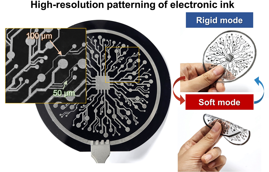
On June 4th, a research team led by Professor Jae-Woong Jeong from the School of Electrical Engineering at KAIST, Professor Seongjun Park from the Digital Healthcare Major at Seoul National University, and Professor Steve Park from the Department of Materials Science and Engineering at KAIST introduced a novel liquid metal electronic ink. This ink allows for micro-scale circuit printing – thinner than a human hair – at room temperature, with the ability to reversibly switch between rigid and soft modes depending on temperature.
The new ink combines printable viscosity with excellent electrical conductivity, enabling the creation of complex, high-resolution multilayer circuits comparable to commercial printed circuit boards (PCBs). These circuits can dynamically change stiffness in response to temperature, presenting new opportunities for multifunctional electronics, medical technologies, and robotics.
Conventional electronics typically have fixed form factors – either rigid for durability or soft for wearability. Rigid devices like smartphones and laptops offer robust performance but are uncomfortable when worn, while soft electronics are more comfortable but lack precise handling. As demand grows for devices that can adapt their stiffness to context, variable-stiffness electronics are becoming increasingly important.
< Figure 1. Fabrication process of stable, high-viscosity electronic ink by dispersing micro-sized gallium particles in a polymer matrix (left). High-resolution large-area circuit printing process through pH-controlled chemical sintering (right). >
To address this challenge, the researchers focused on gallium, which melts just below body temperature. Solid gallium is quite stiff, while its liquid form is fluid and soft. Despite its potential, gallium’s use in electronic printing has been limited by its high surface tension and instability when melted.
To overcome these issues, the team developed a pH-controlled liquid metal ink printing process. By dispersing micro-sized gallium particles into a hydrophilic polyurethane matrix using a neutral solvent (dimethyl sulfoxide, or DMSO), they created a stable, high-viscosity ink suitable for precision printing. During post-print heating, the DMSO decomposes to form an acidic environment, which removes the oxide layer on the gallium particles. This triggers the particles to coalesce into electrically conductive networks with tunable mechanical properties.
The resulting printed circuits exhibit fine feature sizes (~50 μm), high conductivity (2.27 × 10⁶ S/m), and a stiffness modulation ratio of up to 1,465 – allowing the material to shift from plastic-like rigidity to rubber-like softness. Furthermore, the ink is compatible with conventional printing techniques such as screen printing and dip coating, supporting large-area and 3D device fabrication.
< Figure 2. Key features of the electronic ink. (i) High-resolution printing and multilayer integration capability. (ii) Batch fabrication capability through large-area screen printing. (iii) Complex three-dimensional structure printing capability through dip coating. (iv) Excellent electrical conductivity and stiffness control capability.>
The team demonstrated this technology by developing a multi-functional device that operates as a rigid portable electronic under normal conditions but transforms into a soft wearable healthcare device when attached to the body. They also created a neural probe that remains stiff during surgical insertion for accurate positioning but softens once inside brain tissue to reduce inflammation – highlighting its potential for biomedical implants.
< Figure 3. Variable stiffness wearable electronics with high-resolution circuits and multilayer structure comparable to commercial printed circuit boards (PCBs). Functions as a rigid portable electronic device at room temperature, then transforms into a wearable healthcare device by softening at body temperature upon skin contact.>
“The core achievement of this research lies in overcoming the longstanding challenges of liquid metal printing through our innovative technology,” said Professor Jeong. “By controlling the ink’s acidity, we were able to electrically and mechanically connect printed gallium particles, enabling the room-temperature fabrication of high-resolution, large-area circuits with tunable stiffness. This opens up new possibilities for future personal electronics, medical devices, and robotics.”
< Figure 4. Body-temperature softening neural probe implemented by coating electronic ink on an optical waveguide structure. (Left) Remains rigid during surgery for precise manipulation and brain insertion, then softens after implantation to minimize mechanical stress on the brain and greatly enhance biocompatibility. (Right) >
This research was published in Science Advances under the title, “Phase-Change Metal Ink with pH-Controlled Chemical Sintering for Versatile and Scalable Fabrication of Variable Stiffness Electronics.” The work was supported by the National Research Foundation of Korea, the Boston-Korea Project, and the BK21 FOUR Program.
2025.06.04 View 3851
KAIST Research Team Develops Electronic Ink for Room-Temperature Printing of High-Resolution, Variable-Stiffness Electronics
A team of researchers from KAIST and Seoul National University has developed a groundbreaking electronic ink that enables room-temperature printing of variable-stiffness circuits capable of switching between rigid and soft modes. This advancement marks a significant leap toward next-generation wearable, implantable, and robotic devices.
< Photo 1. (From left) Professor Jae-Woong Jeong and PhD candidate Simok Lee of the School of Electrical Engineering, (in separate bubbles, from left) Professor Gun-Hee Lee of Pusan National University, Professor Seongjun Park of Seoul National University, Professor Steve Park of the Department of Materials Science and Engineering>
Variable-stiffness electronics are at the forefront of adaptive technology, offering the ability for a single device to transition between rigid and soft modes depending on its use case. Gallium, a metal known for its high rigidity contrast between solid and liquid states, is a promising candidate for such applications. However, its use has been hindered by challenges including high surface tension, low viscosity, and undesirable phase transitions during manufacturing.
On June 4th, a research team led by Professor Jae-Woong Jeong from the School of Electrical Engineering at KAIST, Professor Seongjun Park from the Digital Healthcare Major at Seoul National University, and Professor Steve Park from the Department of Materials Science and Engineering at KAIST introduced a novel liquid metal electronic ink. This ink allows for micro-scale circuit printing – thinner than a human hair – at room temperature, with the ability to reversibly switch between rigid and soft modes depending on temperature.
The new ink combines printable viscosity with excellent electrical conductivity, enabling the creation of complex, high-resolution multilayer circuits comparable to commercial printed circuit boards (PCBs). These circuits can dynamically change stiffness in response to temperature, presenting new opportunities for multifunctional electronics, medical technologies, and robotics.
Conventional electronics typically have fixed form factors – either rigid for durability or soft for wearability. Rigid devices like smartphones and laptops offer robust performance but are uncomfortable when worn, while soft electronics are more comfortable but lack precise handling. As demand grows for devices that can adapt their stiffness to context, variable-stiffness electronics are becoming increasingly important.
< Figure 1. Fabrication process of stable, high-viscosity electronic ink by dispersing micro-sized gallium particles in a polymer matrix (left). High-resolution large-area circuit printing process through pH-controlled chemical sintering (right). >
To address this challenge, the researchers focused on gallium, which melts just below body temperature. Solid gallium is quite stiff, while its liquid form is fluid and soft. Despite its potential, gallium’s use in electronic printing has been limited by its high surface tension and instability when melted.
To overcome these issues, the team developed a pH-controlled liquid metal ink printing process. By dispersing micro-sized gallium particles into a hydrophilic polyurethane matrix using a neutral solvent (dimethyl sulfoxide, or DMSO), they created a stable, high-viscosity ink suitable for precision printing. During post-print heating, the DMSO decomposes to form an acidic environment, which removes the oxide layer on the gallium particles. This triggers the particles to coalesce into electrically conductive networks with tunable mechanical properties.
The resulting printed circuits exhibit fine feature sizes (~50 μm), high conductivity (2.27 × 10⁶ S/m), and a stiffness modulation ratio of up to 1,465 – allowing the material to shift from plastic-like rigidity to rubber-like softness. Furthermore, the ink is compatible with conventional printing techniques such as screen printing and dip coating, supporting large-area and 3D device fabrication.
< Figure 2. Key features of the electronic ink. (i) High-resolution printing and multilayer integration capability. (ii) Batch fabrication capability through large-area screen printing. (iii) Complex three-dimensional structure printing capability through dip coating. (iv) Excellent electrical conductivity and stiffness control capability.>
The team demonstrated this technology by developing a multi-functional device that operates as a rigid portable electronic under normal conditions but transforms into a soft wearable healthcare device when attached to the body. They also created a neural probe that remains stiff during surgical insertion for accurate positioning but softens once inside brain tissue to reduce inflammation – highlighting its potential for biomedical implants.
< Figure 3. Variable stiffness wearable electronics with high-resolution circuits and multilayer structure comparable to commercial printed circuit boards (PCBs). Functions as a rigid portable electronic device at room temperature, then transforms into a wearable healthcare device by softening at body temperature upon skin contact.>
“The core achievement of this research lies in overcoming the longstanding challenges of liquid metal printing through our innovative technology,” said Professor Jeong. “By controlling the ink’s acidity, we were able to electrically and mechanically connect printed gallium particles, enabling the room-temperature fabrication of high-resolution, large-area circuits with tunable stiffness. This opens up new possibilities for future personal electronics, medical devices, and robotics.”
< Figure 4. Body-temperature softening neural probe implemented by coating electronic ink on an optical waveguide structure. (Left) Remains rigid during surgery for precise manipulation and brain insertion, then softens after implantation to minimize mechanical stress on the brain and greatly enhance biocompatibility. (Right) >
This research was published in Science Advances under the title, “Phase-Change Metal Ink with pH-Controlled Chemical Sintering for Versatile and Scalable Fabrication of Variable Stiffness Electronics.” The work was supported by the National Research Foundation of Korea, the Boston-Korea Project, and the BK21 FOUR Program.
2025.06.04 View 3851 -
 Professor Hyun Myung's Team Wins First Place in a Challenge at ICRA by IEEE
< Photo 1. (From left) Daebeom Kim (Team Leader, Ph.D. student), Seungjae Lee (Ph.D. student), Seoyeon Jang (Ph.D. student), Jei Kong (Master's student), Professor Hyun Myung >
A team of the Urban Robotics Lab, led by Professor Hyun Myung from the KAIST School of Electrical Engineering, achieved a remarkable first-place overall victory in the Nothing Stands Still Challenge (NSS Challenge) 2025, held at the 2025 IEEE International Conference on Robotics and Automation (ICRA), the world's most prestigious robotics conference, from May 19 to 23 in Atlanta, USA.
The NSS Challenge was co-hosted by HILTI, a global construction company based in Liechtenstein, and Stanford University's Gradient Spaces Group. It is an expanded version of the HILTI SLAM (Simultaneous Localization and Mapping)* Challenge, which has been held since 2021, and is considered one of the most prominent challenges at 2025 IEEE ICRA.*SLAM: Refers to Simultaneous Localization and Mapping, a technology where robots, drones, autonomous vehicles, etc., determine their own position and simultaneously create a map of their surroundings.
< Photo 2. A scene from the oral presentation on the winning team's technology (Speakers: Seungjae Lee and Seoyeon Jang, Ph.D. candidates of KAIST School of Electrical Engineering) >
This challenge primarily evaluates how accurately and robustly LiDAR scan data, collected at various times, can be registered in situations with frequent structural changes, such as construction and industrial environments. In particular, it is regarded as a highly technical competition because it deals with multi-session localization and mapping (Multi-session SLAM) technology that responds to structural changes occurring over multiple timeframes, rather than just single-point registration accuracy.
The Urban Robotics Lab team secured first place overall, surpassing National Taiwan University (3rd place) and Northwestern Polytechnical University of China (2nd place) by a significant margin, with their unique localization and mapping technology that solves the problem of registering LiDAR data collected across multiple times and spaces. The winning team will be awarded a prize of $4,000.
< Figure 1. Example of Multiway-Registration for Registering Multiple Scans >
The Urban Robotics Lab team independently developed a multiway-registration framework that can robustly register multiple scans even without prior connection information. This framework consists of an algorithm for summarizing feature points within scans and finding correspondences (CubicFeat), an algorithm for performing global registration based on the found correspondences (Quatro), and an algorithm for refining results based on change detection (Chamelion). This combination of technologies ensures stable registration performance based on fixed structures, even in highly dynamic industrial environments.
< Figure 2. Example of Change Detection Using the Chamelion Algorithm>
LiDAR scan registration technology is a core component of SLAM (Simultaneous Localization And Mapping) in various autonomous systems such as autonomous vehicles, autonomous robots, autonomous walking systems, and autonomous flying vehicles.
Professor Hyun Myung of the School of Electrical Engineering stated, "This award-winning technology is evaluated as a case that simultaneously proves both academic value and industrial applicability by maximizing the performance of precisely estimating the relative positions between different scans even in complex environments. I am grateful to the students who challenged themselves and never gave up, even when many teams abandoned due to the high difficulty."
< Figure 3. Competition Result Board, Lower RMSE (Root Mean Squared Error) Indicates Higher Score (Unit: meters)>
The Urban Robotics Lab team first participated in the SLAM Challenge in 2022, winning second place among academic teams, and in 2023, they secured first place overall in the LiDAR category and first place among academic teams in the vision category.
2025.05.30 View 4613
Professor Hyun Myung's Team Wins First Place in a Challenge at ICRA by IEEE
< Photo 1. (From left) Daebeom Kim (Team Leader, Ph.D. student), Seungjae Lee (Ph.D. student), Seoyeon Jang (Ph.D. student), Jei Kong (Master's student), Professor Hyun Myung >
A team of the Urban Robotics Lab, led by Professor Hyun Myung from the KAIST School of Electrical Engineering, achieved a remarkable first-place overall victory in the Nothing Stands Still Challenge (NSS Challenge) 2025, held at the 2025 IEEE International Conference on Robotics and Automation (ICRA), the world's most prestigious robotics conference, from May 19 to 23 in Atlanta, USA.
The NSS Challenge was co-hosted by HILTI, a global construction company based in Liechtenstein, and Stanford University's Gradient Spaces Group. It is an expanded version of the HILTI SLAM (Simultaneous Localization and Mapping)* Challenge, which has been held since 2021, and is considered one of the most prominent challenges at 2025 IEEE ICRA.*SLAM: Refers to Simultaneous Localization and Mapping, a technology where robots, drones, autonomous vehicles, etc., determine their own position and simultaneously create a map of their surroundings.
< Photo 2. A scene from the oral presentation on the winning team's technology (Speakers: Seungjae Lee and Seoyeon Jang, Ph.D. candidates of KAIST School of Electrical Engineering) >
This challenge primarily evaluates how accurately and robustly LiDAR scan data, collected at various times, can be registered in situations with frequent structural changes, such as construction and industrial environments. In particular, it is regarded as a highly technical competition because it deals with multi-session localization and mapping (Multi-session SLAM) technology that responds to structural changes occurring over multiple timeframes, rather than just single-point registration accuracy.
The Urban Robotics Lab team secured first place overall, surpassing National Taiwan University (3rd place) and Northwestern Polytechnical University of China (2nd place) by a significant margin, with their unique localization and mapping technology that solves the problem of registering LiDAR data collected across multiple times and spaces. The winning team will be awarded a prize of $4,000.
< Figure 1. Example of Multiway-Registration for Registering Multiple Scans >
The Urban Robotics Lab team independently developed a multiway-registration framework that can robustly register multiple scans even without prior connection information. This framework consists of an algorithm for summarizing feature points within scans and finding correspondences (CubicFeat), an algorithm for performing global registration based on the found correspondences (Quatro), and an algorithm for refining results based on change detection (Chamelion). This combination of technologies ensures stable registration performance based on fixed structures, even in highly dynamic industrial environments.
< Figure 2. Example of Change Detection Using the Chamelion Algorithm>
LiDAR scan registration technology is a core component of SLAM (Simultaneous Localization And Mapping) in various autonomous systems such as autonomous vehicles, autonomous robots, autonomous walking systems, and autonomous flying vehicles.
Professor Hyun Myung of the School of Electrical Engineering stated, "This award-winning technology is evaluated as a case that simultaneously proves both academic value and industrial applicability by maximizing the performance of precisely estimating the relative positions between different scans even in complex environments. I am grateful to the students who challenged themselves and never gave up, even when many teams abandoned due to the high difficulty."
< Figure 3. Competition Result Board, Lower RMSE (Root Mean Squared Error) Indicates Higher Score (Unit: meters)>
The Urban Robotics Lab team first participated in the SLAM Challenge in 2022, winning second place among academic teams, and in 2023, they secured first place overall in the LiDAR category and first place among academic teams in the vision category.
2025.05.30 View 4613 -
 KAIST Captures Protein Reaction in Just Six Milliseconds
Understanding biomolecular processes - such as protein-protein interactions and enzyme-substrate reactions that occur on the microseconds to millisecond time scale is essential for comprehending life processes and advancing drug development. KAIST researchers have developed a method for freezing and analyzing biochemical reaction dynamics within a span of just a few milliseconds, marking a significant step forward in better understanding complex biological reactions.
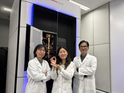
< Photo. (From left) Professor Jin Young Kang and Haerang Hwang of the Integrated Master's and Doctoral Program of the Department of Chemistry, along with Professor Wonhee Lee of the Department of Physics >
KAIST (represented by President Kwang Hyung Lee) announced on the 24th of March that a joint research team led by Professor Jin Young Kang from the Department of Chemistry and Professor Wonhee Lee from the Department of Physics has developed a parylene-based thin-film microfluidic mixing-and-spraying device for ultra-fast biochemical reaction studies.
*Parylene: A key material for microfluidic devices used to observe protein dynamics at ultra-high speeds. It can be fabricated into a few micrometer-thick films, which can be used in making a spray nozzle for microfluidic devices.
This research overcomes the limitations of the existing time-resolved cryo-electron microscopy (TRCEM) method by reducing sample consumption to one-third of the conventional amount while improving the minimum time resolution—down to just six milliseconds (6 ms).
TRCEM is a technique that rapidly freezes protein complexes during intermediate reaction stages under cryogenic conditions, which allows researchers to analyze their structures. This approach has gained significant attention recently for its ability to capture transient biochemical events.
< Figure 1. Time-resolved cryo-EM (TRCEM) technique using microfluidic channels. In order to capture the intermediate structure of biomolecules during a biochemical reaction over time, biomolecules and reaction substrates are mixed in a microfluidic channel, and then sprayed on a grid after a certain reaction time and frozen in liquid ethane to prepare a cryo-EM sample. This can then be analyzed by cryo-EM to observe the structural changes of proteins over time. >
Transient intermediate structures of protein complexes could not be captured by traditional cryo-electron microscopy due to their extremely short lifespans. Although several TRCEM techniques have been developed to address this issue, previous methods were hindered by large sample consumption and limited time resolution. To overcome these challenges, the KAIST team developed a new mixing-and-spraying device using ultra-thin parylene films. The integrated design of the device further enhanced the precision and reproducibility of experiments.
< Figure 2. TRCEM grid fabrication setup using a parylene-based thin-film microfluidic device and actual appearance of the device. You can see that a thin-film parylene channel is inserted into the injection nozzle. The integration of the reaction channel and the injection nozzle allowed the residence time in the device to be reduced to at least 0.5 ms. >
“This research makes TRCEM more practical and paves the way for diverse applications of the parylene thin-film device in structural biology, drug development, enzyme reaction studies, and biosensor research.” Professor Jin Young Kang explained, emphasizing the significance of the study.
Professor Wonhee Lee added, “The team aims to continue this research, focusing on improvement of the technique to achieve higher time resolution with minimal sample consumption.”
< Figure 3. Comparison of the spraying patterns of the parylene mixing-jet device and the conventional mixing-jet device and the filament length in the resulting RecA-ssDNA filament formation reaction. It was shown that the thin film spray nozzle structure affects the uniformity and accuracy of the final reaction time. >
The research findings, with Haerang Hwang (a graduate student in the integrated master's and Ph.D. program in the Department of Chemistry) as the first author, were published online on January 28, 2025, in the international journal Advanced Functional Materials. (Paper Title: “Integrated Parylene-Based Thin-Film Microfluidic Device for Time-Resolved Cryo-Electron Microscopy”, DOI: doi.org/10.1002/adfm.202418224)
This research was supported by the National Research Foundation of Korea (NRF), the Samsung Future Technology Development Program, and the CELINE consortium.
2025.03.24 View 4888
KAIST Captures Protein Reaction in Just Six Milliseconds
Understanding biomolecular processes - such as protein-protein interactions and enzyme-substrate reactions that occur on the microseconds to millisecond time scale is essential for comprehending life processes and advancing drug development. KAIST researchers have developed a method for freezing and analyzing biochemical reaction dynamics within a span of just a few milliseconds, marking a significant step forward in better understanding complex biological reactions.
< Photo. (From left) Professor Jin Young Kang and Haerang Hwang of the Integrated Master's and Doctoral Program of the Department of Chemistry, along with Professor Wonhee Lee of the Department of Physics >
KAIST (represented by President Kwang Hyung Lee) announced on the 24th of March that a joint research team led by Professor Jin Young Kang from the Department of Chemistry and Professor Wonhee Lee from the Department of Physics has developed a parylene-based thin-film microfluidic mixing-and-spraying device for ultra-fast biochemical reaction studies.
*Parylene: A key material for microfluidic devices used to observe protein dynamics at ultra-high speeds. It can be fabricated into a few micrometer-thick films, which can be used in making a spray nozzle for microfluidic devices.
This research overcomes the limitations of the existing time-resolved cryo-electron microscopy (TRCEM) method by reducing sample consumption to one-third of the conventional amount while improving the minimum time resolution—down to just six milliseconds (6 ms).
TRCEM is a technique that rapidly freezes protein complexes during intermediate reaction stages under cryogenic conditions, which allows researchers to analyze their structures. This approach has gained significant attention recently for its ability to capture transient biochemical events.
< Figure 1. Time-resolved cryo-EM (TRCEM) technique using microfluidic channels. In order to capture the intermediate structure of biomolecules during a biochemical reaction over time, biomolecules and reaction substrates are mixed in a microfluidic channel, and then sprayed on a grid after a certain reaction time and frozen in liquid ethane to prepare a cryo-EM sample. This can then be analyzed by cryo-EM to observe the structural changes of proteins over time. >
Transient intermediate structures of protein complexes could not be captured by traditional cryo-electron microscopy due to their extremely short lifespans. Although several TRCEM techniques have been developed to address this issue, previous methods were hindered by large sample consumption and limited time resolution. To overcome these challenges, the KAIST team developed a new mixing-and-spraying device using ultra-thin parylene films. The integrated design of the device further enhanced the precision and reproducibility of experiments.
< Figure 2. TRCEM grid fabrication setup using a parylene-based thin-film microfluidic device and actual appearance of the device. You can see that a thin-film parylene channel is inserted into the injection nozzle. The integration of the reaction channel and the injection nozzle allowed the residence time in the device to be reduced to at least 0.5 ms. >
“This research makes TRCEM more practical and paves the way for diverse applications of the parylene thin-film device in structural biology, drug development, enzyme reaction studies, and biosensor research.” Professor Jin Young Kang explained, emphasizing the significance of the study.
Professor Wonhee Lee added, “The team aims to continue this research, focusing on improvement of the technique to achieve higher time resolution with minimal sample consumption.”
< Figure 3. Comparison of the spraying patterns of the parylene mixing-jet device and the conventional mixing-jet device and the filament length in the resulting RecA-ssDNA filament formation reaction. It was shown that the thin film spray nozzle structure affects the uniformity and accuracy of the final reaction time. >
The research findings, with Haerang Hwang (a graduate student in the integrated master's and Ph.D. program in the Department of Chemistry) as the first author, were published online on January 28, 2025, in the international journal Advanced Functional Materials. (Paper Title: “Integrated Parylene-Based Thin-Film Microfluidic Device for Time-Resolved Cryo-Electron Microscopy”, DOI: doi.org/10.1002/adfm.202418224)
This research was supported by the National Research Foundation of Korea (NRF), the Samsung Future Technology Development Program, and the CELINE consortium.
2025.03.24 View 4888 -
 KAIST Captures Hot Holes: A Breakthrough in Light-to-Electricity Energy Conversion
When light interacts with metallic nanostructures, it instantaneously generates plasmonic hot carriers, which serve as key intermediates for converting optical energy into high-value energy sources such as electricity and chemical energy. Among these, hot holes play a crucial role in enhancing photoelectrochemical reactions. However, they thermally dissipate within picoseconds (trillionths of a second), making practical applications challenging. Now, a Korean research team has successfully developed a method for sustaining hot holes longer and amplifying their flow, accelerating the commercialization of next-generation, high-efficiency, light-to-energy conversion technologies.
KAIST (represented by President Kwang Hyung Lee) announced on the 12th of March that a research team led by Distinguished Professor Jeong Young Park from the Department of Chemistry, in collaboration with Professor Moonsang Lee from the Department of Materials Science and Engineering at Inha University, has successfully amplified the flow of hot holes and mapped local current distribution in real time, thereby elucidating the mechanism of photocurrent enhancement.
The team designed a nanodiode structure by placing a metallic nanomesh on a specialized semiconductor substrate (p-type gallium nitride) to facilitate hot hole extraction at the surface. As a result, in gallium nitride substrates aligned with the hot hole extraction direction, the flow of hot holes was amplified by approximately two times compared to substrates aligned in other directions.
To fabricate the Au nanomesh, a polystyrene nano-bead monolayer assembly was first placed on a gallium nitride (p-GaN) substrate, and then the polystyrene nano-beads were etched to form a nanomesh template (Figure 1A). Then, a 20 nm thick gold nano-film was deposited, and the etched polystyrene nano-beads were removed to realize the gold nano-mesh structure on the GaN substrate (Figure 1B). The fabricated Au nanomesh exhibited strong light absorption in the visible range due to the plasmonic resonance effect (Figure 1C). >
Furthermore, using a photoconductive atomic force microscopy (pc-AFM)-based photocurrent mapping system, the researchers analyzed the flow of hot holes in real time at the nanometer scale (one hundred-thousandth the thickness of a human hair). They observed that hot hole activation was strongest at "hot spots," where light was locally concentrated on the gold nanomesh. However, by modifying the growth direction of the gallium nitride substrate, hot hole activation extended beyond the hot spots to other areas as well.
Through this research, the team discovered an efficient method for converting light into electrical and chemical energy. This breakthrough is expected to significantly advance next-generation solar cells, photocatalysts, and hydrogen production technologies.
Professor Jeong Young Park stated, "For the first time, we have successfully controlled the flow of hot holes using a nanodiode technique. This innovation holds great potential for various optoelectronic devices and photocatalytic applications. For example, it could lead to groundbreaking advancements in solar energy conversion technologies, such as solar cells and hydrogen production. Additionally, the real-time analysis technology we developed can be applied to the development of ultra-miniaturized optoelectronic devices, including optical sensors and nanoscale semiconductor components."
The study was led by Hyunhwa Lee (PhD., KAIST Department of Chemistry) and Yujin Park (Postdoc Researcher, University of Texas at Austin Department of Chemical Engineering) as co-first authors and Professors Moonsang Lee (Inha University, Department of Materials Science and Engineering) and Jeong Young Park (KAIST, Department of Chemistry) serving as corresponding authors. The research findings were published online in Science Advances on March 7.
(Paper Title: “Reconfiguring hot-hole flux via polarity modulation of p-GaN in plasmonic Schottky architectures”, DOI: https://www.science.org/doi/10.1126/sciadv.adu0086)
This research was supported by the National Research Foundation of Korea (NRF).
2025.03.17 View 5003
KAIST Captures Hot Holes: A Breakthrough in Light-to-Electricity Energy Conversion
When light interacts with metallic nanostructures, it instantaneously generates plasmonic hot carriers, which serve as key intermediates for converting optical energy into high-value energy sources such as electricity and chemical energy. Among these, hot holes play a crucial role in enhancing photoelectrochemical reactions. However, they thermally dissipate within picoseconds (trillionths of a second), making practical applications challenging. Now, a Korean research team has successfully developed a method for sustaining hot holes longer and amplifying their flow, accelerating the commercialization of next-generation, high-efficiency, light-to-energy conversion technologies.
KAIST (represented by President Kwang Hyung Lee) announced on the 12th of March that a research team led by Distinguished Professor Jeong Young Park from the Department of Chemistry, in collaboration with Professor Moonsang Lee from the Department of Materials Science and Engineering at Inha University, has successfully amplified the flow of hot holes and mapped local current distribution in real time, thereby elucidating the mechanism of photocurrent enhancement.
The team designed a nanodiode structure by placing a metallic nanomesh on a specialized semiconductor substrate (p-type gallium nitride) to facilitate hot hole extraction at the surface. As a result, in gallium nitride substrates aligned with the hot hole extraction direction, the flow of hot holes was amplified by approximately two times compared to substrates aligned in other directions.
To fabricate the Au nanomesh, a polystyrene nano-bead monolayer assembly was first placed on a gallium nitride (p-GaN) substrate, and then the polystyrene nano-beads were etched to form a nanomesh template (Figure 1A). Then, a 20 nm thick gold nano-film was deposited, and the etched polystyrene nano-beads were removed to realize the gold nano-mesh structure on the GaN substrate (Figure 1B). The fabricated Au nanomesh exhibited strong light absorption in the visible range due to the plasmonic resonance effect (Figure 1C). >
Furthermore, using a photoconductive atomic force microscopy (pc-AFM)-based photocurrent mapping system, the researchers analyzed the flow of hot holes in real time at the nanometer scale (one hundred-thousandth the thickness of a human hair). They observed that hot hole activation was strongest at "hot spots," where light was locally concentrated on the gold nanomesh. However, by modifying the growth direction of the gallium nitride substrate, hot hole activation extended beyond the hot spots to other areas as well.
Through this research, the team discovered an efficient method for converting light into electrical and chemical energy. This breakthrough is expected to significantly advance next-generation solar cells, photocatalysts, and hydrogen production technologies.
Professor Jeong Young Park stated, "For the first time, we have successfully controlled the flow of hot holes using a nanodiode technique. This innovation holds great potential for various optoelectronic devices and photocatalytic applications. For example, it could lead to groundbreaking advancements in solar energy conversion technologies, such as solar cells and hydrogen production. Additionally, the real-time analysis technology we developed can be applied to the development of ultra-miniaturized optoelectronic devices, including optical sensors and nanoscale semiconductor components."
The study was led by Hyunhwa Lee (PhD., KAIST Department of Chemistry) and Yujin Park (Postdoc Researcher, University of Texas at Austin Department of Chemical Engineering) as co-first authors and Professors Moonsang Lee (Inha University, Department of Materials Science and Engineering) and Jeong Young Park (KAIST, Department of Chemistry) serving as corresponding authors. The research findings were published online in Science Advances on March 7.
(Paper Title: “Reconfiguring hot-hole flux via polarity modulation of p-GaN in plasmonic Schottky architectures”, DOI: https://www.science.org/doi/10.1126/sciadv.adu0086)
This research was supported by the National Research Foundation of Korea (NRF).
2025.03.17 View 5003 -
 A 20-year-old puzzle solved: KAIST research team reveals the 'three-dimensional vortex' of zero-dimensional ferroelectrics
Materials that can maintain a magnetized state by themselves without an external magnetic field (i.e., permanent magnets) are called ferromagnets. Ferroelectrics can be thought of as the electric counterpart to ferromagnets, as they maintain a polarized state without an external electric field. It is well-known that ferromagnets lose their magnetic properties when reduced to nano sizes below a certain threshold. What happens when ferroelectrics are similarly made extremely small in all directions (i.e., into a zero-dimensional structure such as nanoparticles) has been a topic of controversy for a long time.
< (From left) Professor Yongsoo Yang, the corresponding author, and Chaehwa Jeong, the first author studying in the integrated master’s and doctoral program, of the KAIST Department of Physics >
The research team led by Dr. Yongsoo Yang from the Department of Physics at KAIST has, for the first time, experimentally clarified the three-dimensional, vortex-shaped polarization distribution inside ferroelectric nanoparticles through international collaborative research with POSTECH, SNU, KBSI, LBNL and University of Arkansas.
About 20 years ago, Prof. Laurent Bellaiche (currently at University of Arkansas) and his colleagues theoretically predicted that a unique form of polarization distribution, arranged in a toroidal vortex shape, could occur inside ferroelectric nanodots. They also suggested that if this vortex distribution could be properly controlled, it could be applied to ultra-high-density memory devices with capacities over 10,000 times greater than existing ones. However, experimental clarification had not been achieved due to the difficulty of measuring the three-dimensional polarization distribution within ferroelectric nanostructures.
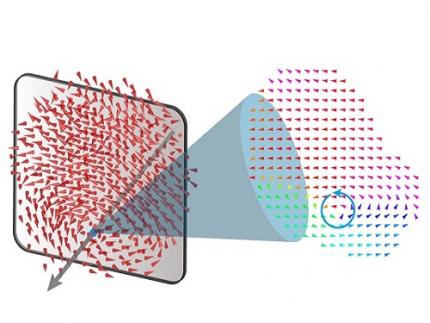
The research team at KAIST successfully solved this 20-year-old challenge by implementing a technique called atomic electron tomography. This technique works by acquiring atomic-resolution transmission electron microscope images of the nanomaterials from multiple tilt angles, and then reconstructing them back into three-dimensional structures using advanced reconstruction algorithms. Electron tomography can be understood as essentially the same method with the CT scans used in hospitals to view internal organs in three dimensions; the KAIST team adapted it uniquely for nanomaterials, utilizing an electron microscope at the single-atom level.
< Figure 1. Three-dimensional polarization distribution of BaTiO3 nanoparticles revealed by atomic electron tomography. >(Left) Schematic of the electron tomography technique, which involves acquiring transmission electron microscope images at multiple tilt angles and reconstructing them into 3D atomic structures.(Center) Experimentally determined three-dimensional polarization distribution inside a BaTiO3 nanoparticle via atomic electron tomography. A vortex-like structure is clearly visible near the bottom (blue dot).(Right) A two-dimensional cross-section of the polarization distribution, thinly sliced at the center of the vortex, with the color and arrows together indicating the direction of the polarization. A distinct vortex structure can be observed.
Using atomic electron tomography, the team completely measured the positions of cation atoms inside barium titanate (BaTiO3) nanoparticles, a well-known ferroelectric material, in three dimensions. From the precisely determined 3D atomic arrangements, they were able to further calculate the internal three-dimensional polarization distribution at the single-atom level. The analysis of the polarization distribution revealed, for the first time experimentally, that topological polarization orderings including vortices, anti-vortices, skyrmions, and a Bloch point occur inside the 0-dimensional ferroelectrics, as theoretically predicted 20 years ago. Furthermore, it was also found that the number of internal vortices can be controlled depending on their sizes.
Prof. Sergey Prosandeev and Prof. Bellaiche (who proposed with other co-workers the polar vortex ordering theoretically 20 years ago), joined this collaboration and further proved that the vortex distribution results obtained from experiments are consistent with theoretical calculations.
By controlling the number and orientation of these polarization distributions, it is expected that this can be utilized into next-generation high-density memory device that can store more than 10,000 times the amount of information in the same-sized device compared to existing ones.
Dr. Yang, who led the research, explained the significance of the results: “This result suggests that controlling the size and shape of ferroelectrics alone, without needing to tune the substrate or surrounding environmental effects such as epitaxial strain, can manipulate ferroelectric vortices or other topological orderings at the nano-scale. Further research could then be applied to the development of next-generation ultra-high-density memory.”
This research, with Chaehwa Jeong from the Department of Physics at KAIST as the first author, was published online in Nature Communications on May 8th (Title: Revealing the Three-Dimensional Arrangement of Polar Topology in Nanoparticles).
The study was mainly supported by the National Research Foundation of Korea (NRF) Grants funded by the Korean Government (MSIT).
2024.05.31 View 8870
A 20-year-old puzzle solved: KAIST research team reveals the 'three-dimensional vortex' of zero-dimensional ferroelectrics
Materials that can maintain a magnetized state by themselves without an external magnetic field (i.e., permanent magnets) are called ferromagnets. Ferroelectrics can be thought of as the electric counterpart to ferromagnets, as they maintain a polarized state without an external electric field. It is well-known that ferromagnets lose their magnetic properties when reduced to nano sizes below a certain threshold. What happens when ferroelectrics are similarly made extremely small in all directions (i.e., into a zero-dimensional structure such as nanoparticles) has been a topic of controversy for a long time.
< (From left) Professor Yongsoo Yang, the corresponding author, and Chaehwa Jeong, the first author studying in the integrated master’s and doctoral program, of the KAIST Department of Physics >
The research team led by Dr. Yongsoo Yang from the Department of Physics at KAIST has, for the first time, experimentally clarified the three-dimensional, vortex-shaped polarization distribution inside ferroelectric nanoparticles through international collaborative research with POSTECH, SNU, KBSI, LBNL and University of Arkansas.
About 20 years ago, Prof. Laurent Bellaiche (currently at University of Arkansas) and his colleagues theoretically predicted that a unique form of polarization distribution, arranged in a toroidal vortex shape, could occur inside ferroelectric nanodots. They also suggested that if this vortex distribution could be properly controlled, it could be applied to ultra-high-density memory devices with capacities over 10,000 times greater than existing ones. However, experimental clarification had not been achieved due to the difficulty of measuring the three-dimensional polarization distribution within ferroelectric nanostructures.
The research team at KAIST successfully solved this 20-year-old challenge by implementing a technique called atomic electron tomography. This technique works by acquiring atomic-resolution transmission electron microscope images of the nanomaterials from multiple tilt angles, and then reconstructing them back into three-dimensional structures using advanced reconstruction algorithms. Electron tomography can be understood as essentially the same method with the CT scans used in hospitals to view internal organs in three dimensions; the KAIST team adapted it uniquely for nanomaterials, utilizing an electron microscope at the single-atom level.
< Figure 1. Three-dimensional polarization distribution of BaTiO3 nanoparticles revealed by atomic electron tomography. >(Left) Schematic of the electron tomography technique, which involves acquiring transmission electron microscope images at multiple tilt angles and reconstructing them into 3D atomic structures.(Center) Experimentally determined three-dimensional polarization distribution inside a BaTiO3 nanoparticle via atomic electron tomography. A vortex-like structure is clearly visible near the bottom (blue dot).(Right) A two-dimensional cross-section of the polarization distribution, thinly sliced at the center of the vortex, with the color and arrows together indicating the direction of the polarization. A distinct vortex structure can be observed.
Using atomic electron tomography, the team completely measured the positions of cation atoms inside barium titanate (BaTiO3) nanoparticles, a well-known ferroelectric material, in three dimensions. From the precisely determined 3D atomic arrangements, they were able to further calculate the internal three-dimensional polarization distribution at the single-atom level. The analysis of the polarization distribution revealed, for the first time experimentally, that topological polarization orderings including vortices, anti-vortices, skyrmions, and a Bloch point occur inside the 0-dimensional ferroelectrics, as theoretically predicted 20 years ago. Furthermore, it was also found that the number of internal vortices can be controlled depending on their sizes.
Prof. Sergey Prosandeev and Prof. Bellaiche (who proposed with other co-workers the polar vortex ordering theoretically 20 years ago), joined this collaboration and further proved that the vortex distribution results obtained from experiments are consistent with theoretical calculations.
By controlling the number and orientation of these polarization distributions, it is expected that this can be utilized into next-generation high-density memory device that can store more than 10,000 times the amount of information in the same-sized device compared to existing ones.
Dr. Yang, who led the research, explained the significance of the results: “This result suggests that controlling the size and shape of ferroelectrics alone, without needing to tune the substrate or surrounding environmental effects such as epitaxial strain, can manipulate ferroelectric vortices or other topological orderings at the nano-scale. Further research could then be applied to the development of next-generation ultra-high-density memory.”
This research, with Chaehwa Jeong from the Department of Physics at KAIST as the first author, was published online in Nature Communications on May 8th (Title: Revealing the Three-Dimensional Arrangement of Polar Topology in Nanoparticles).
The study was mainly supported by the National Research Foundation of Korea (NRF) Grants funded by the Korean Government (MSIT).
2024.05.31 View 8870 -
 KAIST Demonstrates AI and sustainable technologies at CES 2024
On January 2, KAIST announced it will be participating in the Consumer Electronics Show (CES) 2024, held between January 9 and 12.
CES 2024 is one of the world’s largest tech conferences to take place in Las Vegas. Under the slogan “KAIST, the Global Value Creator” for its exhibition, KAIST has submitted technologies falling under one of following themes: “Expansion of Human Intelligence, Mobility, and Reality”, and “Pursuit of Human Security and Sustainable Development”.
24 startups and pre-startups whose technologies stand out in various fields including artificial intelligence (AI), mobility, virtual reality, healthcare and human security, and sustainable development, will welcome their visitors at an exclusive booth of 232 m2 prepared for KAIST at Eureka Park in Las Vegas.
12 businesses will participate in the first category, “Expansion of Human Intelligence, Mobility, and Reality”, including MicroPix, Panmnesia, DeepAuto, MGL, Reports, Narnia Labs, EL FACTORY, Korea Position Technology, AudAi, Planby Technologies, Movin, and Studio Lab.
In the “Pursuit of Human Security and Sustainable Development” category, 12 businesses including Aldaver, ADNC, Solve, Iris, Blue Device, Barreleye, TR, A2US, Greeners, Iron Boys, Shard Partners and Kingbot, will be introduced.
In particular, Aldaver is a startup that received the Korean Business Award 2023 as well as the presidential award at the Challenge K-Startup with its biomimetic material and printing technology. It has attracted 4.5 billion KRW of investment thus far.
Narnia Labs, with its AI design solution for manufacturing, won the grand prize for K-tech Startups 2022, and has so far attracted 3.5 billion KRW of investments.
Panmnesia is a startup that won the 2024 CES Innovation Award, recognized for their fab-less AI semiconductor technology. They attracted 16 billion KRW of investment through seed round alone.
Meanwhile, student startups will also be presented during the exhibition. Studio Lab received a CES 2024 Best of Innovation Award in the AI category. The team developed the software Seller Canvas, which automatically generates a page for product details when a user uploads an image of a product.
The central stage at the KAIST exhibition booth will be used to interview members of the participating startups between Jan 9 to 11, as well as a networking site for businesses and invited investors during KAIST NIGHT on the evening of 10th, between 5 and 7 PM.
Director Sung-Yool Choi of the KAIST Institute of Technology Value Creation said, “Through CES 2024, KAIST will overcome the limits of human intelligence, mobility, and space with the deep-tech based technologies developed by its startups, and will demonstrate its achievements for realizing its vision as a global value-creating university through the solutions for human security and sustainable development.”
2024.01.05 View 12849
KAIST Demonstrates AI and sustainable technologies at CES 2024
On January 2, KAIST announced it will be participating in the Consumer Electronics Show (CES) 2024, held between January 9 and 12.
CES 2024 is one of the world’s largest tech conferences to take place in Las Vegas. Under the slogan “KAIST, the Global Value Creator” for its exhibition, KAIST has submitted technologies falling under one of following themes: “Expansion of Human Intelligence, Mobility, and Reality”, and “Pursuit of Human Security and Sustainable Development”.
24 startups and pre-startups whose technologies stand out in various fields including artificial intelligence (AI), mobility, virtual reality, healthcare and human security, and sustainable development, will welcome their visitors at an exclusive booth of 232 m2 prepared for KAIST at Eureka Park in Las Vegas.
12 businesses will participate in the first category, “Expansion of Human Intelligence, Mobility, and Reality”, including MicroPix, Panmnesia, DeepAuto, MGL, Reports, Narnia Labs, EL FACTORY, Korea Position Technology, AudAi, Planby Technologies, Movin, and Studio Lab.
In the “Pursuit of Human Security and Sustainable Development” category, 12 businesses including Aldaver, ADNC, Solve, Iris, Blue Device, Barreleye, TR, A2US, Greeners, Iron Boys, Shard Partners and Kingbot, will be introduced.
In particular, Aldaver is a startup that received the Korean Business Award 2023 as well as the presidential award at the Challenge K-Startup with its biomimetic material and printing technology. It has attracted 4.5 billion KRW of investment thus far.
Narnia Labs, with its AI design solution for manufacturing, won the grand prize for K-tech Startups 2022, and has so far attracted 3.5 billion KRW of investments.
Panmnesia is a startup that won the 2024 CES Innovation Award, recognized for their fab-less AI semiconductor technology. They attracted 16 billion KRW of investment through seed round alone.
Meanwhile, student startups will also be presented during the exhibition. Studio Lab received a CES 2024 Best of Innovation Award in the AI category. The team developed the software Seller Canvas, which automatically generates a page for product details when a user uploads an image of a product.
The central stage at the KAIST exhibition booth will be used to interview members of the participating startups between Jan 9 to 11, as well as a networking site for businesses and invited investors during KAIST NIGHT on the evening of 10th, between 5 and 7 PM.
Director Sung-Yool Choi of the KAIST Institute of Technology Value Creation said, “Through CES 2024, KAIST will overcome the limits of human intelligence, mobility, and space with the deep-tech based technologies developed by its startups, and will demonstrate its achievements for realizing its vision as a global value-creating university through the solutions for human security and sustainable development.”
2024.01.05 View 12849 -
 KAIST to showcase a pack of KAIST Start-ups at CES 2023
- KAIST is to run an Exclusive Booth at the Venetian Expo (Hall G) in Eureka Park, at CES 2023, to be held in Las Vegas from Thursday, January 5th through Sunday, the 8th.
- Twelve businesses recently put together by KAIST faculty, alumni, and the start-ups given legal usage of KAIST technologies will be showcased.
- Out of the participating start-ups, the products by Fluiz and Hills Robotics were selected as the “CES Innovation Award 2023 Honoree”, scoring top in their respective categories.
On January 3, KAIST announced that there will be a KAIST booth at Consumer Electronics Show (CES) 2023, the most influential tech event in the world, to be held in Las Vegas from January 3 to 8.
At this exclusive corner, KAIST will introduce the technologies of KAIST start-ups over the exhibition period.
KAIST first started holding its exclusive booth in CES 2019 with five start-up businesses, following up at CES 2020 with 12 start-ups and at CES 2022 with 10 start-ups. At CES 2023, which would be KAIST’s fourth conference, KAIST will be accompanying 12 businesses including start-ups by the faculty members, alumni, and technology transfer companies that just began their businesses with technologies from their research findings that stands a head above others.
To maximize the publicity opportunity, KAIST will support each company’s marketing strategies through cooperation with the Korea International Trade Association (KITA), and provide an opportunity for the school and each startup to create global identity and exhibit the excellence of their technologies at the convention.
The following companies will be at the KAIST Booth in Eureka Park:
The twelve startups mentioned above aim to achieve global technology commecialization in their respective fields of expertise spanning from eXtended Reality (XR) and gaming, to AI and robotics, vehicle and transport, mobile platform, smart city, autonomous driving, healthcare, internet of thing (IoT), through joint research and development, technology transfer and investment attraction from world’s leading institutions and enterprises.
In particular, Fluiz and Hills Robotics won the CES Innovation Award as 2023 Honorees and is expected to attain greater achievements in the future.
A staff member from the KAIST Institute of Technology Value Creation said, “The KAIST Showcase for CES 2023 has prepared a new pitching space for each of the companies for their own IR efforts, and we hope that KAIST startups will actively and effectively market their products and technologies while they are at the convention. We hope it will help them utilize their time here to establish their name in presence here which will eventually serve as a good foothold for them and their predecessors to further global commercialization goals.”
2023.01.04 View 19481
KAIST to showcase a pack of KAIST Start-ups at CES 2023
- KAIST is to run an Exclusive Booth at the Venetian Expo (Hall G) in Eureka Park, at CES 2023, to be held in Las Vegas from Thursday, January 5th through Sunday, the 8th.
- Twelve businesses recently put together by KAIST faculty, alumni, and the start-ups given legal usage of KAIST technologies will be showcased.
- Out of the participating start-ups, the products by Fluiz and Hills Robotics were selected as the “CES Innovation Award 2023 Honoree”, scoring top in their respective categories.
On January 3, KAIST announced that there will be a KAIST booth at Consumer Electronics Show (CES) 2023, the most influential tech event in the world, to be held in Las Vegas from January 3 to 8.
At this exclusive corner, KAIST will introduce the technologies of KAIST start-ups over the exhibition period.
KAIST first started holding its exclusive booth in CES 2019 with five start-up businesses, following up at CES 2020 with 12 start-ups and at CES 2022 with 10 start-ups. At CES 2023, which would be KAIST’s fourth conference, KAIST will be accompanying 12 businesses including start-ups by the faculty members, alumni, and technology transfer companies that just began their businesses with technologies from their research findings that stands a head above others.
To maximize the publicity opportunity, KAIST will support each company’s marketing strategies through cooperation with the Korea International Trade Association (KITA), and provide an opportunity for the school and each startup to create global identity and exhibit the excellence of their technologies at the convention.
The following companies will be at the KAIST Booth in Eureka Park:
The twelve startups mentioned above aim to achieve global technology commecialization in their respective fields of expertise spanning from eXtended Reality (XR) and gaming, to AI and robotics, vehicle and transport, mobile platform, smart city, autonomous driving, healthcare, internet of thing (IoT), through joint research and development, technology transfer and investment attraction from world’s leading institutions and enterprises.
In particular, Fluiz and Hills Robotics won the CES Innovation Award as 2023 Honorees and is expected to attain greater achievements in the future.
A staff member from the KAIST Institute of Technology Value Creation said, “The KAIST Showcase for CES 2023 has prepared a new pitching space for each of the companies for their own IR efforts, and we hope that KAIST startups will actively and effectively market their products and technologies while they are at the convention. We hope it will help them utilize their time here to establish their name in presence here which will eventually serve as a good foothold for them and their predecessors to further global commercialization goals.”
2023.01.04 View 19481 -
 Metabolically Engineered Bacterium Produces Lutein
A research group at KAIST has engineered a bacterial strain capable of producing lutein. The research team applied systems metabolic engineering strategies, including substrate channeling and electron channeling, to enhance the production of lutein in an engineered Escherichia coli strain. The strategies will be also useful for the efficient production of other industrially important natural products used in the food, pharmaceutical, and cosmetic industries.
Figure: Systems metabolic engineering was employed to construct and optimize the metabolic pathways for lutein production, and substrate channeling and electron channeling strategies were additionally employed to increase the production of the lutein with high productivity.
Lutein is classified as a xanthophyll chemical that is abundant in egg yolk, fruits, and vegetables. It protects the eye from oxidative damage from radiation and reduces the risk of eye diseases including macular degeneration and cataracts. Commercialized products featuring lutein are derived from the extracts of the marigold flower, which is known to harbor abundant amounts of lutein. However, the drawback of lutein production from nature is that it takes a long time to grow and harvest marigold flowers. Furthermore, it requires additional physical and chemical-based extractions with a low yield, which makes it economically unfeasible in terms of productivity. The high cost and low yield of these bioprocesses has made it difficult to readily meet the demand for lutein.
These challenges inspired the metabolic engineers at KAIST, including researchers Dr. Seon Young Park, Ph.D. Candidate Hyunmin Eun, and Distinguished Professor Sang Yup Lee from the Department of Chemical and Biomolecular Engineering. The team’s study entitled “Metabolic engineering of Escherichia coli with electron channeling for the production of natural products” was published in Nature Catalysis on August 5, 2022.
This research details the ability to produce lutein from E. coli with a high yield using a cheap carbon source, glycerol, via systems metabolic engineering. The research group focused on solving the bottlenecks of the biosynthetic pathway for lutein production constructed within an individual cell. First, using systems metabolic engineering, which is an integrated technology to engineer the metabolism of a microorganism, lutein was produced when the lutein biosynthesis pathway was introduced, albeit in very small amounts.
To improve the productivity of lutein production, the bottleneck enzymes within the metabolic pathway were first identified. It turned out that metabolic reactions that involve a promiscuous enzyme, an enzyme that is involved in two or more metabolic reactions, and electron-requiring cytochrome P450 enzymes are the main bottleneck steps of the pathway inhibiting lutein biosynthesis.
To overcome these challenges, substrate channeling, a strategy to artificially recruit enzymes in physical proximity within the cell in order to increase the local concentrations of substrates that can be converted into products, was employed to channel more metabolic flux towards the target chemical while reducing the formation of unwanted byproducts.
Furthermore, electron channeling, a strategy similar to substrate channeling but differing in terms of increasing the local concentrations of electrons required for oxidoreduction reactions mediated by P450 and its reductase partners, was applied to further streamline the metabolic flux towards lutein biosynthesis, which led to the highest titer of lutein production achieved in a bacterial host ever reported. The same electron channeling strategy was successfully applied for the production of other natural products including nootkatone and apigenin in E. coli, showcasing the general applicability of the strategy in the research field.
“It is expected that this microbial cell factory-based production of lutein will be able to replace the current plant extraction-based process,” said Dr. Seon Young Park, the first author of the paper. She explained that another important point of the research is that integrated metabolic engineering strategies developed from this study can be generally applicable for the efficient production of other natural products useful as pharmaceuticals or nutraceuticals.
“As maintaining good health in an aging society is becoming increasingly important, we expect that the technology and strategies developed here will play pivotal roles in producing other valuable natural products of medical or nutritional importance,” explained Distinguished Professor Sang Yup Lee.
This work was supported by the Cooperative Research Program for Agriculture Science & Technology Development funded by the Rural Development Administration of Korea, with further support from the Development of Next-generation Biorefinery Platform Technologies for Leading Bio-based Chemicals Industry Project and by the Development of Platform Technologies of Microbial Cell Factories for the Next-generation Biorefineries Project of the National Research Foundation funded by the Ministry of Science and ICT of Korea.
2022.08.05 View 12351
Metabolically Engineered Bacterium Produces Lutein
A research group at KAIST has engineered a bacterial strain capable of producing lutein. The research team applied systems metabolic engineering strategies, including substrate channeling and electron channeling, to enhance the production of lutein in an engineered Escherichia coli strain. The strategies will be also useful for the efficient production of other industrially important natural products used in the food, pharmaceutical, and cosmetic industries.
Figure: Systems metabolic engineering was employed to construct and optimize the metabolic pathways for lutein production, and substrate channeling and electron channeling strategies were additionally employed to increase the production of the lutein with high productivity.
Lutein is classified as a xanthophyll chemical that is abundant in egg yolk, fruits, and vegetables. It protects the eye from oxidative damage from radiation and reduces the risk of eye diseases including macular degeneration and cataracts. Commercialized products featuring lutein are derived from the extracts of the marigold flower, which is known to harbor abundant amounts of lutein. However, the drawback of lutein production from nature is that it takes a long time to grow and harvest marigold flowers. Furthermore, it requires additional physical and chemical-based extractions with a low yield, which makes it economically unfeasible in terms of productivity. The high cost and low yield of these bioprocesses has made it difficult to readily meet the demand for lutein.
These challenges inspired the metabolic engineers at KAIST, including researchers Dr. Seon Young Park, Ph.D. Candidate Hyunmin Eun, and Distinguished Professor Sang Yup Lee from the Department of Chemical and Biomolecular Engineering. The team’s study entitled “Metabolic engineering of Escherichia coli with electron channeling for the production of natural products” was published in Nature Catalysis on August 5, 2022.
This research details the ability to produce lutein from E. coli with a high yield using a cheap carbon source, glycerol, via systems metabolic engineering. The research group focused on solving the bottlenecks of the biosynthetic pathway for lutein production constructed within an individual cell. First, using systems metabolic engineering, which is an integrated technology to engineer the metabolism of a microorganism, lutein was produced when the lutein biosynthesis pathway was introduced, albeit in very small amounts.
To improve the productivity of lutein production, the bottleneck enzymes within the metabolic pathway were first identified. It turned out that metabolic reactions that involve a promiscuous enzyme, an enzyme that is involved in two or more metabolic reactions, and electron-requiring cytochrome P450 enzymes are the main bottleneck steps of the pathway inhibiting lutein biosynthesis.
To overcome these challenges, substrate channeling, a strategy to artificially recruit enzymes in physical proximity within the cell in order to increase the local concentrations of substrates that can be converted into products, was employed to channel more metabolic flux towards the target chemical while reducing the formation of unwanted byproducts.
Furthermore, electron channeling, a strategy similar to substrate channeling but differing in terms of increasing the local concentrations of electrons required for oxidoreduction reactions mediated by P450 and its reductase partners, was applied to further streamline the metabolic flux towards lutein biosynthesis, which led to the highest titer of lutein production achieved in a bacterial host ever reported. The same electron channeling strategy was successfully applied for the production of other natural products including nootkatone and apigenin in E. coli, showcasing the general applicability of the strategy in the research field.
“It is expected that this microbial cell factory-based production of lutein will be able to replace the current plant extraction-based process,” said Dr. Seon Young Park, the first author of the paper. She explained that another important point of the research is that integrated metabolic engineering strategies developed from this study can be generally applicable for the efficient production of other natural products useful as pharmaceuticals or nutraceuticals.
“As maintaining good health in an aging society is becoming increasingly important, we expect that the technology and strategies developed here will play pivotal roles in producing other valuable natural products of medical or nutritional importance,” explained Distinguished Professor Sang Yup Lee.
This work was supported by the Cooperative Research Program for Agriculture Science & Technology Development funded by the Rural Development Administration of Korea, with further support from the Development of Next-generation Biorefinery Platform Technologies for Leading Bio-based Chemicals Industry Project and by the Development of Platform Technologies of Microbial Cell Factories for the Next-generation Biorefineries Project of the National Research Foundation funded by the Ministry of Science and ICT of Korea.
2022.08.05 View 12351