%73%65%6e%73%6f%72
-
 KAIST Opens the Era of “Space Sensors” with Optical Functions Reconfigurable by Electrical Signals Alone
Until now, satellites and space payloads have required new optical filters and sensors to be designed whenever their missions changed. A future is now on the horizon in which a single ultra-compact optical chip can perform a variety of roles—including those of a thermal imaging sensor, spectrometer, and infrared camera—using electrical signals alone.
KAIST (President Choongsik Bae) announced on 14th of July that a research team led by Professor Hyun Jung Kim from the Department of Aerospace Engineering, in collaboration with a research team led by Professor Juejun Hu at the Massachusetts Institute of Technology (MIT), has demonstrated the first transmissive mid-infrared amplitude-only spatial light modulator based on a scalable two-dimensional, electrically addressable metasurface architecture.
The key achievement of this research is that a single optical chip can perform a variety of sensor functions using electrical signals alone. Previously, new optical filters and sensors had to be fabricated for each new mission. In the future, the technology is expected to enable the realization of “software-defined sensors,” whose functions can be changed without replacing the hardware.
The device developed by the research team is a transmissive mid-infrared spatial light modulator, or SLM, based on a metasurface. A metasurface is an ultrathin optical structure that uses microscopic patterns much smaller than the width of a human hair to freely control the intensity, direction, and wavelength of light.
A spatial light modulator controls the spatial distribution of light on a pixel-by-pixel basis. In the present device, each pixel switches the intensity of transmitted mid-infrared light between two programmed states. The research team succeeded, for the first time in the world, in electrically and independently controlling each individual pixel.
Conventional spatial light modulators face significant limitations in the mid-infrared. Liquid-crystal-based devices suffer from material absorption and relatively slow response, while digital micromirror devices operate in reflection. Transmissive mid-infrared SLMs have therefore remained largely unexplored. This has limited their application to satellite sensors, ultra-compact spectrometers—which analyze light according to wavelength—and adaptive optical systems, which automatically adjust their optical performance in response to changes in the surrounding environment.
To address these limitations, the researchers used GSST—Ge₂Sb₂Se₄Te, or germanium-antimony-selenium-tellurium—an optical phase-change material (PCM) whose light transmittance changes when it receives an electrical signal.
Once GSST receives an electrical signal, it retains its state and continues to maintain the same optical performance even after the power is turned off. This nonvolatile characteristic eliminates the need for a continuous power supply, making the material suitable for satellites and space payloads, where the available electrical power is limited.
As the number of pixels on an optical chip increases, electrical current can flow into pixels other than the selected pixel, causing unintended pixels to operate as well. This is known as the “sneak-path” problem.
The research team solved this problem by integrating a silicon PIN diode into each pixel. A PIN diode is a semiconductor device that allows electrical current to flow only to the intended pixel. This enabled the researchers to accurately select and control only the desired pixels.
Using this approach, the team independently controlled all the pixels in a 6 × 6 pixel array and successfully produced desired optical patterns. The device also maintained stable performance after more than 16,700 switching cycles, demonstrating approximately 13 times greater endurance than previous technology.
The device was fabricated using silicon photonics, a technology that produces optical devices through standard semiconductor manufacturing processes. This makes it relatively easy to scale the technology to larger optical chips containing hundreds, thousands, or even more pixels.
The current device controls only the amount of transmitted light. In the future, however, more sophisticated metasurface designs are expected to enable the technology to develop into “universal reconfigurable optics,” capable of freely controlling the direction and polarization of light as well.
The greatest significance of this research is that it presents a new concept in which “optics, too, can be changed like software.” In other words, the study provides a foundation for programmable optical hardware that could support different sensing functions through reconfiguration rather than hardware replacement. In the future, this is expected to usher in an era of software-defined sensors, in which a single optical chip can perform different functions depending on the situation, serving as a thermal imaging sensor, spectrometer, infrared camera, or optical communication device.
Once commercialized, the technology is expected to make it possible to implement a wide range of optical systems on a single platform. Potential applications include satellites and space payloads, launch-vehicle health diagnostics, thermal monitoring of space stations, measurement of in-space manufacturing processes, infrared imaging, and optical communications.
This research is an achievement that further advances MIT–NASA collaborative research initiated in 2018, when Professor Hyun Jung Kim was working as a researcher at the National Aeronautics and Space Administration (NASA), and subsequently continued at KAIST.
Building on this foundation, KAIST’s STAR Lab and Professor Juejun Hu’s research team at MIT are currently conducting joint research on active meta-optics, silicon photonics, and space sensor systems, with the goal of applying the technology in actual space environments.
The two teams have established a full-cycle international collaborative research framework encompassing material development, chip design and fabrication, sensor-system integration, space-environment verification, and future flight demonstrations.
Professor Kim’s research team is now developing the technology into an operational space sensor. Under the Ministry of Science and ICT’s Young Researcher Program, the team is developing an ultra-precise system for measuring the surface temperature of launch vehicles.
The research is also being expanded through the “Space Services and Manufacturing Research Center” under the Innovation Research Center Program. The team is conducting research to develop the technology into a common optical platform that can be used for space-station thermal monitoring, anomaly diagnosis, measurement of in-space manufacturing processes, and optical communications.
“This research is not simply about creating one more new optical device,” said Professor Kim. “It presents the foundation for an era of software-defined sensors, in which a single optical chip performs a variety of functions depending on the mission.”
“By combining MIT’s nanophotonics technology—which uses nanostructures to control light—with KAIST’s space sensor technology, we plan to develop this technology into an actual space system,” she added. The research was published online in the international journal Nature Communications on July 7.
Paper title: “Two-Dimensional Pixel-Level Addressable Mid-Infrared Metasurface Spatial Light Modulator”
DOI: 10.1038/s41467-026-75346-5
This work was funded by the Air Force SBIR Program under contract FA2394-23-C-5076, the National Science Foundation under awards 2329088 and 2132929, and National Research Foundation of Korea (NRF) grant funded by the Korea government (MSIT) (RS-2025-00515651 and RS-2025-02213804).
2026.07.14 View 294
KAIST Opens the Era of “Space Sensors” with Optical Functions Reconfigurable by Electrical Signals Alone
Until now, satellites and space payloads have required new optical filters and sensors to be designed whenever their missions changed. A future is now on the horizon in which a single ultra-compact optical chip can perform a variety of roles—including those of a thermal imaging sensor, spectrometer, and infrared camera—using electrical signals alone.
KAIST (President Choongsik Bae) announced on 14th of July that a research team led by Professor Hyun Jung Kim from the Department of Aerospace Engineering, in collaboration with a research team led by Professor Juejun Hu at the Massachusetts Institute of Technology (MIT), has demonstrated the first transmissive mid-infrared amplitude-only spatial light modulator based on a scalable two-dimensional, electrically addressable metasurface architecture.
The key achievement of this research is that a single optical chip can perform a variety of sensor functions using electrical signals alone. Previously, new optical filters and sensors had to be fabricated for each new mission. In the future, the technology is expected to enable the realization of “software-defined sensors,” whose functions can be changed without replacing the hardware.
The device developed by the research team is a transmissive mid-infrared spatial light modulator, or SLM, based on a metasurface. A metasurface is an ultrathin optical structure that uses microscopic patterns much smaller than the width of a human hair to freely control the intensity, direction, and wavelength of light.
A spatial light modulator controls the spatial distribution of light on a pixel-by-pixel basis. In the present device, each pixel switches the intensity of transmitted mid-infrared light between two programmed states. The research team succeeded, for the first time in the world, in electrically and independently controlling each individual pixel.
Conventional spatial light modulators face significant limitations in the mid-infrared. Liquid-crystal-based devices suffer from material absorption and relatively slow response, while digital micromirror devices operate in reflection. Transmissive mid-infrared SLMs have therefore remained largely unexplored. This has limited their application to satellite sensors, ultra-compact spectrometers—which analyze light according to wavelength—and adaptive optical systems, which automatically adjust their optical performance in response to changes in the surrounding environment.
To address these limitations, the researchers used GSST—Ge₂Sb₂Se₄Te, or germanium-antimony-selenium-tellurium—an optical phase-change material (PCM) whose light transmittance changes when it receives an electrical signal.
Once GSST receives an electrical signal, it retains its state and continues to maintain the same optical performance even after the power is turned off. This nonvolatile characteristic eliminates the need for a continuous power supply, making the material suitable for satellites and space payloads, where the available electrical power is limited.
As the number of pixels on an optical chip increases, electrical current can flow into pixels other than the selected pixel, causing unintended pixels to operate as well. This is known as the “sneak-path” problem.
The research team solved this problem by integrating a silicon PIN diode into each pixel. A PIN diode is a semiconductor device that allows electrical current to flow only to the intended pixel. This enabled the researchers to accurately select and control only the desired pixels.
Using this approach, the team independently controlled all the pixels in a 6 × 6 pixel array and successfully produced desired optical patterns. The device also maintained stable performance after more than 16,700 switching cycles, demonstrating approximately 13 times greater endurance than previous technology.
The device was fabricated using silicon photonics, a technology that produces optical devices through standard semiconductor manufacturing processes. This makes it relatively easy to scale the technology to larger optical chips containing hundreds, thousands, or even more pixels.
The current device controls only the amount of transmitted light. In the future, however, more sophisticated metasurface designs are expected to enable the technology to develop into “universal reconfigurable optics,” capable of freely controlling the direction and polarization of light as well.
The greatest significance of this research is that it presents a new concept in which “optics, too, can be changed like software.” In other words, the study provides a foundation for programmable optical hardware that could support different sensing functions through reconfiguration rather than hardware replacement. In the future, this is expected to usher in an era of software-defined sensors, in which a single optical chip can perform different functions depending on the situation, serving as a thermal imaging sensor, spectrometer, infrared camera, or optical communication device.
Once commercialized, the technology is expected to make it possible to implement a wide range of optical systems on a single platform. Potential applications include satellites and space payloads, launch-vehicle health diagnostics, thermal monitoring of space stations, measurement of in-space manufacturing processes, infrared imaging, and optical communications.
This research is an achievement that further advances MIT–NASA collaborative research initiated in 2018, when Professor Hyun Jung Kim was working as a researcher at the National Aeronautics and Space Administration (NASA), and subsequently continued at KAIST.
Building on this foundation, KAIST’s STAR Lab and Professor Juejun Hu’s research team at MIT are currently conducting joint research on active meta-optics, silicon photonics, and space sensor systems, with the goal of applying the technology in actual space environments.
The two teams have established a full-cycle international collaborative research framework encompassing material development, chip design and fabrication, sensor-system integration, space-environment verification, and future flight demonstrations.
Professor Kim’s research team is now developing the technology into an operational space sensor. Under the Ministry of Science and ICT’s Young Researcher Program, the team is developing an ultra-precise system for measuring the surface temperature of launch vehicles.
The research is also being expanded through the “Space Services and Manufacturing Research Center” under the Innovation Research Center Program. The team is conducting research to develop the technology into a common optical platform that can be used for space-station thermal monitoring, anomaly diagnosis, measurement of in-space manufacturing processes, and optical communications.
“This research is not simply about creating one more new optical device,” said Professor Kim. “It presents the foundation for an era of software-defined sensors, in which a single optical chip performs a variety of functions depending on the mission.”
“By combining MIT’s nanophotonics technology—which uses nanostructures to control light—with KAIST’s space sensor technology, we plan to develop this technology into an actual space system,” she added. The research was published online in the international journal Nature Communications on July 7.
Paper title: “Two-Dimensional Pixel-Level Addressable Mid-Infrared Metasurface Spatial Light Modulator”
DOI: 10.1038/s41467-026-75346-5
This work was funded by the Air Force SBIR Program under contract FA2394-23-C-5076, the National Science Foundation under awards 2329088 and 2132929, and National Research Foundation of Korea (NRF) grant funded by the Korea government (MSIT) (RS-2025-00515651 and RS-2025-02213804).
2026.07.14 View 294 -
 KAIST Develops Next-Generation Self-Powered Wearable Sensor Resilient to 668% Elongation
Wearable medical devices that monitor heart rate, respiration, and joint movements for long periods without battery concerns, electronic skins that sense external stimuli like human skin, and soft robots made of flexible materials that move freely have all come one step closer to reality. KAIST researchers have developed a self-powered sensor (a sensor that generates electricity on its own without a battery) that can stretch up to 668% while producing stable electrical signals.
KAIST announced on June 18th that a research team led by Professor Miso Kim from the Department of Mechanical Engineering has overcome the durability limitations of conventional piezoelectric fiber sensors (fiber-type sensors that convert pressure or movement into electrical signals) and successfully developed a highly stretchable piezoelectric fiber sensor that operates stably even under repeated deformation.
The core material of the sensor, piezoelectric polymer, is a polymeric material that generates electricity when subjected to mechanical force. Although its lightweight and flexible nature makes it suitable for skin-attachable wearable sensors, conventional piezoelectric fiber sensors suffered from signal degradation during repeated stretching or bending, as the electrode layer collecting electrical signals and the piezoelectric layer generating electricity would become damaged. Furthermore, while coiling the fibers can increase stretchability to allow greater elongation, maintaining electrical stability remained a significant challenge.
To resolve these issues, the research team developed a "Hierarchical Resilient Design" strategy, engineering the sensor to withstand deformation across multiple levels—from its constituent materials and electrodes to its overall structure. Simply put, just as a rubber band returns to its original shape after repeated stretching, the sensor is designed to self-maintain its performance after cyclical deformation.
First, the research team embedded elastic polymer microparticles inside the piezoelectric nanofibers to create a closely interlocking structure. This creates a supportive effect similar to Velcro, helping the sensor recover its original shape even after being repeatedly stretched.
Additionally, they designed the interface so that the electricity-collecting electrode and the electricity-generating piezoelectric layer connect seamlessly. By strongly bonding different materials together, they ensured they would not easily delaminate under impact or deformation, allowing the sensor to maintain a stable electrical signal even when significantly stretched or bent.
Applying this design to a coil structure, the research team successfully stretched the sensor up to 668%—approximately 6.7 times its original length—while maintaining a stable output. The developed sensor generated consistent electrical signals under various movements, including stretching, bending, and pressing.
Furthermore, the research team fabricated the sensor not only in coil forms but also in knot configurations, confirming its stable operation under repeated forces or sudden impacts. By leveraging artificial intelligence (AI) to analyze the sensor signals, they were also able to accurately distinguish between different movements, such as pressing, bending, and stretching.
This study holds great significance as it presents a self-powered sensor platform that simultaneously achieves high stretchability and long-term stability without requiring a battery. In particular, because it enables stable signal measurement in environments undergoing repeated deformation, it is expected to be utilized in developing next-generation wearable medical devices for long-term monitoring of various biosignals, including heart rate, respiration, joint movement, and muscle activity. It is also projected to expand its range of applications to digital healthcare devices, electronic skins, and sensory sensors for soft robots by making devices lighter and more convenient to use.
"The core achievement of this research is that it simultaneously secured mechanical resilience and electrical reliability by combining fiber structure design with electrode interface engineering (a technology that controls the boundary where different materials meet)," said Professor Miso Kim. She added, "In the future, we expect it to be applied to wearable medical devices requiring long-term wear, electronic skins, and sensory sensors for soft robots, enabling more accurate and continuous biosignal monitoring."
The research findings, with researcher Yong Jun Choi as the first author, were published on March 10, 2026, in ACS Nano (Impact Factor 16.1), a world-renowned academic journal in the fields of nanotechnology and materials science.
Paper Title: Mechanically and Functionally Resilient Piezoelectric Fiber Coils and Knots for Reliable Self-Powered Sensing DOI: doi/10.1021/acsnano.5c19628 Author Information: Yong Jun Choi 1 (KAIST, First Author), JungHun Park 1 (KAIST, Co-author), Jisoo Nam 1 (KAIST, Co-author), Gi-Dong Sim 1 (KAIST, Co-author), Myung-Gil Kim 2 (Sungkyunkwan University, Co-author), Miso Kim (KAIST, Corresponding Author)
This research was conducted with support from the BRIDGE Convergence Research and Development Program (RS-2023-00254689), the Nano·Material Technology Development Program (RS-2024-00468995), and the Next-Generation Semiconductor-Compatible Micro-Substrate Technology Development Program (RS-2024-00433654) funded by the National Research Foundation of Korea under the Ministry of Science and ICT.
2026.06.18 View 2249
KAIST Develops Next-Generation Self-Powered Wearable Sensor Resilient to 668% Elongation
Wearable medical devices that monitor heart rate, respiration, and joint movements for long periods without battery concerns, electronic skins that sense external stimuli like human skin, and soft robots made of flexible materials that move freely have all come one step closer to reality. KAIST researchers have developed a self-powered sensor (a sensor that generates electricity on its own without a battery) that can stretch up to 668% while producing stable electrical signals.
KAIST announced on June 18th that a research team led by Professor Miso Kim from the Department of Mechanical Engineering has overcome the durability limitations of conventional piezoelectric fiber sensors (fiber-type sensors that convert pressure or movement into electrical signals) and successfully developed a highly stretchable piezoelectric fiber sensor that operates stably even under repeated deformation.
The core material of the sensor, piezoelectric polymer, is a polymeric material that generates electricity when subjected to mechanical force. Although its lightweight and flexible nature makes it suitable for skin-attachable wearable sensors, conventional piezoelectric fiber sensors suffered from signal degradation during repeated stretching or bending, as the electrode layer collecting electrical signals and the piezoelectric layer generating electricity would become damaged. Furthermore, while coiling the fibers can increase stretchability to allow greater elongation, maintaining electrical stability remained a significant challenge.
To resolve these issues, the research team developed a "Hierarchical Resilient Design" strategy, engineering the sensor to withstand deformation across multiple levels—from its constituent materials and electrodes to its overall structure. Simply put, just as a rubber band returns to its original shape after repeated stretching, the sensor is designed to self-maintain its performance after cyclical deformation.
First, the research team embedded elastic polymer microparticles inside the piezoelectric nanofibers to create a closely interlocking structure. This creates a supportive effect similar to Velcro, helping the sensor recover its original shape even after being repeatedly stretched.
Additionally, they designed the interface so that the electricity-collecting electrode and the electricity-generating piezoelectric layer connect seamlessly. By strongly bonding different materials together, they ensured they would not easily delaminate under impact or deformation, allowing the sensor to maintain a stable electrical signal even when significantly stretched or bent.
Applying this design to a coil structure, the research team successfully stretched the sensor up to 668%—approximately 6.7 times its original length—while maintaining a stable output. The developed sensor generated consistent electrical signals under various movements, including stretching, bending, and pressing.
Furthermore, the research team fabricated the sensor not only in coil forms but also in knot configurations, confirming its stable operation under repeated forces or sudden impacts. By leveraging artificial intelligence (AI) to analyze the sensor signals, they were also able to accurately distinguish between different movements, such as pressing, bending, and stretching.
This study holds great significance as it presents a self-powered sensor platform that simultaneously achieves high stretchability and long-term stability without requiring a battery. In particular, because it enables stable signal measurement in environments undergoing repeated deformation, it is expected to be utilized in developing next-generation wearable medical devices for long-term monitoring of various biosignals, including heart rate, respiration, joint movement, and muscle activity. It is also projected to expand its range of applications to digital healthcare devices, electronic skins, and sensory sensors for soft robots by making devices lighter and more convenient to use.
"The core achievement of this research is that it simultaneously secured mechanical resilience and electrical reliability by combining fiber structure design with electrode interface engineering (a technology that controls the boundary where different materials meet)," said Professor Miso Kim. She added, "In the future, we expect it to be applied to wearable medical devices requiring long-term wear, electronic skins, and sensory sensors for soft robots, enabling more accurate and continuous biosignal monitoring."
The research findings, with researcher Yong Jun Choi as the first author, were published on March 10, 2026, in ACS Nano (Impact Factor 16.1), a world-renowned academic journal in the fields of nanotechnology and materials science.
Paper Title: Mechanically and Functionally Resilient Piezoelectric Fiber Coils and Knots for Reliable Self-Powered Sensing DOI: doi/10.1021/acsnano.5c19628 Author Information: Yong Jun Choi 1 (KAIST, First Author), JungHun Park 1 (KAIST, Co-author), Jisoo Nam 1 (KAIST, Co-author), Gi-Dong Sim 1 (KAIST, Co-author), Myung-Gil Kim 2 (Sungkyunkwan University, Co-author), Miso Kim (KAIST, Corresponding Author)
This research was conducted with support from the BRIDGE Convergence Research and Development Program (RS-2023-00254689), the Nano·Material Technology Development Program (RS-2024-00468995), and the Next-Generation Semiconductor-Compatible Micro-Substrate Technology Development Program (RS-2024-00433654) funded by the National Research Foundation of Korea under the Ministry of Science and ICT.
2026.06.18 View 2249 -
 A Breakthrough Concept in Nano-Printing Technology
<(From Left) Professor Inkyu Park, Ph.D candidate Byung-Ho Kang, Researcher Jun-Ho Jeong, Professor Junseong Ahn>
A breakthrough technology has been developed that allows metal circuits floating on water to be transferred directly onto any desired surface. A South Korean research team has introduced a novel technique capable of transferring ultra-fine nano-circuits onto plant leaves and fruits, as well as curved automotive surfaces and robot exteriors, all without causing any damage. This technology is expected to be widely utilized across various cutting-edge industries, including smart agriculture, wearable healthcare, and bioelectronics.
KAIST announced on June 15th that a joint research team led by Distinguished Professor Inkyu Park from the Department of Mechanical Engineering, Dr. Jun-Ho Jeong from the Korea Institute of Machinery and Materials and Professor Junseong Ahn from Korea University has successfully developed "Water-Floating Nano-Transfer Printing (WF-nTP)." This technology enables precision metal thin films floated on water to be transferred onto various 3D surfaces.
Conventional nano-transfer printing (nTP), which is widely used to manufacture electronic devices and sensors, typically requires high heat, intense pressure, adhesives, or toxic chemical solvents. Consequently, applying this method to biological tissues or complex curved surfaces that are sensitive to heat and pressure has proven highly challenging.
To overcome these limitations, the research team proposed a completely new approach: floating metal circuits on the surface of water.
Fabrication: The team deposited an ultra-thin layer of metals such as gold (Au), platinum (Pt), palladium (Pd), or nickel (Ni) onto a polymer mold.
Separation: They then used plasma gas which has a high-energy state of ionized gas to selectively remove (etch) a part of the mold.
Floating: When this structure is placed in water, water infiltrates through the microscopic gaps, causing the 20-nanometer (nm) thick metal film to float to the surface on its own while perfectly maintaining its original shape.
<Overview of the water-floated nano mesh and versatile transfer technique>
The research team transferred the metal circuits using a "scooping" method, which involves submerging the target object beneath the floating film and slowly lifting it upward. As the water evaporates, capillary force (the force that moves liquid through narrow spaces) tightly adheres the circuit to the surface. Once the water completely dries, intermolecular forces come into play, securing the circuit firmly in place without the need for any adhesive.
Notably, the team also succeeded in transferring circuits onto hydrophobic (water-repellent) surfaces, such as lotus leaves. By adding a small amount of ethanol to the water to lower its surface tension (the property of a liquid surface that causes it to shrink), they effectively overcame a major limitation of conventional technologies.
This technology holds immense potential for widespread application because it can adapt to diverse surfaces while flawlessly preserving the nano-patterns. Using this method, the research team fabricated Surface-Enhanced Raman Scattering (SERS) sensors which are used for high-sensitivity detection of trace chemical substances and attached them directly to plant leaves and fruit surfaces. Through this, they successfully detected thiram, a pesticide component, on the surfaces of leaves and fruits. Furthermore, they successfully implemented a wearable, high-performance hydrogen gas sensor by transferring a palladium (Pd) mesh onto highly flexible thermoplastic polyurethane (TPU) fibers.
<Research Image(AI-generated)>
Distinguished Professor Inkyu Park stated: "This technology is highly significant as it shatters the substrate limitations of conventional nano-transfer printing, allowing nano-patterns to be transferred onto sensitive surfaces like living plant leaves or human skin without heat or adhesives. We expect it to evolve into a core platform technology for wearable sensors and bioelectronics, finding applications in smart agriculture for pesticide detection without damaging crops, wearable health monitoring devices, bioelectronic devices, and electronic skins for next-generation robots."
This research, with PhD student Byung-Ho Kang from the KAIST Department of Mechanical Engineering participating as the first author, was published online on March 30, 2026, in the prestigious international academic journal Nature Communications.
The study authors include Byung-Ho Kang, Ji-Hwan Ha, Yeongjae Kwon, Sohee Jeon, Donho Lee, Byeongmin Kang, Soon Hyoung Hwang, Junseong Ahn, Jun-Ho Jeong, and Inkyu Park.
Meanwhile, this research was conducted with funding from the Ministry of Science and ICT through the National Research Foundation of Korea (NRF) Mid-Career Researcher Support Program, and the Ministry of Trade, Industry and Energy through the Korea Evaluation Institute of Industrial Technology (KEIT) Alchemist Project.
2026.06.15 View 1608
A Breakthrough Concept in Nano-Printing Technology
<(From Left) Professor Inkyu Park, Ph.D candidate Byung-Ho Kang, Researcher Jun-Ho Jeong, Professor Junseong Ahn>
A breakthrough technology has been developed that allows metal circuits floating on water to be transferred directly onto any desired surface. A South Korean research team has introduced a novel technique capable of transferring ultra-fine nano-circuits onto plant leaves and fruits, as well as curved automotive surfaces and robot exteriors, all without causing any damage. This technology is expected to be widely utilized across various cutting-edge industries, including smart agriculture, wearable healthcare, and bioelectronics.
KAIST announced on June 15th that a joint research team led by Distinguished Professor Inkyu Park from the Department of Mechanical Engineering, Dr. Jun-Ho Jeong from the Korea Institute of Machinery and Materials and Professor Junseong Ahn from Korea University has successfully developed "Water-Floating Nano-Transfer Printing (WF-nTP)." This technology enables precision metal thin films floated on water to be transferred onto various 3D surfaces.
Conventional nano-transfer printing (nTP), which is widely used to manufacture electronic devices and sensors, typically requires high heat, intense pressure, adhesives, or toxic chemical solvents. Consequently, applying this method to biological tissues or complex curved surfaces that are sensitive to heat and pressure has proven highly challenging.
To overcome these limitations, the research team proposed a completely new approach: floating metal circuits on the surface of water.
Fabrication: The team deposited an ultra-thin layer of metals such as gold (Au), platinum (Pt), palladium (Pd), or nickel (Ni) onto a polymer mold.
Separation: They then used plasma gas which has a high-energy state of ionized gas to selectively remove (etch) a part of the mold.
Floating: When this structure is placed in water, water infiltrates through the microscopic gaps, causing the 20-nanometer (nm) thick metal film to float to the surface on its own while perfectly maintaining its original shape.
<Overview of the water-floated nano mesh and versatile transfer technique>
The research team transferred the metal circuits using a "scooping" method, which involves submerging the target object beneath the floating film and slowly lifting it upward. As the water evaporates, capillary force (the force that moves liquid through narrow spaces) tightly adheres the circuit to the surface. Once the water completely dries, intermolecular forces come into play, securing the circuit firmly in place without the need for any adhesive.
Notably, the team also succeeded in transferring circuits onto hydrophobic (water-repellent) surfaces, such as lotus leaves. By adding a small amount of ethanol to the water to lower its surface tension (the property of a liquid surface that causes it to shrink), they effectively overcame a major limitation of conventional technologies.
This technology holds immense potential for widespread application because it can adapt to diverse surfaces while flawlessly preserving the nano-patterns. Using this method, the research team fabricated Surface-Enhanced Raman Scattering (SERS) sensors which are used for high-sensitivity detection of trace chemical substances and attached them directly to plant leaves and fruit surfaces. Through this, they successfully detected thiram, a pesticide component, on the surfaces of leaves and fruits. Furthermore, they successfully implemented a wearable, high-performance hydrogen gas sensor by transferring a palladium (Pd) mesh onto highly flexible thermoplastic polyurethane (TPU) fibers.
<Research Image(AI-generated)>
Distinguished Professor Inkyu Park stated: "This technology is highly significant as it shatters the substrate limitations of conventional nano-transfer printing, allowing nano-patterns to be transferred onto sensitive surfaces like living plant leaves or human skin without heat or adhesives. We expect it to evolve into a core platform technology for wearable sensors and bioelectronics, finding applications in smart agriculture for pesticide detection without damaging crops, wearable health monitoring devices, bioelectronic devices, and electronic skins for next-generation robots."
This research, with PhD student Byung-Ho Kang from the KAIST Department of Mechanical Engineering participating as the first author, was published online on March 30, 2026, in the prestigious international academic journal Nature Communications.
The study authors include Byung-Ho Kang, Ji-Hwan Ha, Yeongjae Kwon, Sohee Jeon, Donho Lee, Byeongmin Kang, Soon Hyoung Hwang, Junseong Ahn, Jun-Ho Jeong, and Inkyu Park.
Meanwhile, this research was conducted with funding from the Ministry of Science and ICT through the National Research Foundation of Korea (NRF) Mid-Career Researcher Support Program, and the Ministry of Trade, Industry and Energy through the Korea Evaluation Institute of Industrial Technology (KEIT) Alchemist Project.
2026.06.15 View 1608 -
 KAIST Develops Real-Time Diagnostic Smart Dressing Patch to End the Fear of Diabetic Foot Amputation
<(From Left) Professor Inkyu Park, Dr. Seokjoo Cho, (Upper Right, From Left) Professor Ji-Hwan Ha, Researcher Jun-Ho Jeong , Professor Wei Gao>
“Diabetic ulcers,” which occur in patients with diabetes, are dangerous complications that can lead to amputation if the treatment window is missed. A joint research team has developed a “smart dressing patch” that can monitor wound conditions in real time.
KAIST (President Kwang Hyung Lee) announced on the 14th of May that a research team led by Distinguished Professor Inkyu Park of the Department of Mechanical Engineering, through joint research with Professor Ji-Hwan Ha of Hanbat National University (President Yongjun Oh), researcher Jun-Ho Jeong of the Korea Institute of Machinery & Materials (President Seog-Hyeon Ryu), and Professor Wei Gao of the California Institute of Technology (Caltech; President Thomas F. Rosenbaum) in the United States, has developed a “wireless, battery-free optoelectronic multi-modal sensor patch” for diabetic ulcer management.
The patch developed by the research team combines an optoelectronic sensor, which can simultaneously measure multiple types of biological information, with a functional dressing. It can analyze glucose concentration, acidity (pH, an indicator of hydrogen ion concentration), and temperature changes at the wound site in real time, and patients can check their condition themselves using a smartphone.
The research team fabricated a functional nanofiber dressing using electrospinning, a method that uses an electric field to create fibers much thinner than a human hair. This dressing changes color in response to increased glucose and changes in acidity that appear in diabetic foot wounds. In other words, if the wound condition worsens, the dressing color changes, allowing danger signals to be easily checked with the naked eye. Through this, abnormal signs that could lead to tissue necrosis can be detected and tracked over long periods in a non-invasive manner, meaning without cutting the skin or drawing blood.
The research team combined this with an optoelectronic system to improve diagnostic accuracy. A light-emitting diode (LED, a semiconductor device that converts electricity into light) embedded in the patch and a photodiode, a semiconductor sensor that detects light, measure the color change of the dressing as light reflectance and then convert it into an electrical signal.
This provides more accurate and stable data than ordinary camera-based imaging because it is less affected by changes in surrounding lighting.
In particular, the patch operates without a separate battery by applying a flexible circuit based on near field communication (NFC), a wireless communication technology that exchanges data over short distances. When a smartphone is placed near the sensor, the patch receives power wirelessly and operates, transmitting the measured data in real time. In other words, patients and medical staff can immediately check and respond to wound conditions using only a smartphone app, without separate complex equipment.
< Conceptual Diagram of a Multimodal Colorimetric Dressing and Optoelectronic Sensor for Diagnosing Diabetic Foot and Diabetic Diseases >
The technology developed in this study has high clinical value because it provides both intuitive visual signals and quantitative electronic data while imposing no physical burden on patients. It is also expected to contribute to improving the quality of life of patients with diabetes by enabling continuous wound management without repeated blood sampling.
Distinguished Professor Inkyu Park stated, “Research that began to reduce the pain of diabetic patients who have to prick their fingers with a needle every day has led to a technology for the preemptive diagnosis of complications,” adding, “This technology will become a core platform technology that can be expanded in the future to blood-free diagnostic technologies not only for diabetes but also for various chronic diseases.”
In this study, KAIST Dr. Seokjoo Cho and Professor Ji-Hwan Ha of Hanbat National University participated as co-first authors. The research results were published on March 26, 2026, in the international materials science journal Advanced Functional Materials. The paper was also selected as a Front Cover article of the journal.
※ Paper title: “Wireless, Battery-Free, Optoelectronic, Multi-Modal Sensor Integrated With Colorimetric Dressing for Diabetic Ulcer Management,” DOI: 10.1002/adfm.202532167
< Front Cover Image >
This research was supported by the Mid-Career Researcher Program of the National Research Foundation of Korea (NRF) funded by the Ministry of Science and ICT, the Alchemist Project of the Ministry of Trade, Industry and Energy, and the Daejeon RISE Center.
2026.05.14 View 2420
KAIST Develops Real-Time Diagnostic Smart Dressing Patch to End the Fear of Diabetic Foot Amputation
<(From Left) Professor Inkyu Park, Dr. Seokjoo Cho, (Upper Right, From Left) Professor Ji-Hwan Ha, Researcher Jun-Ho Jeong , Professor Wei Gao>
“Diabetic ulcers,” which occur in patients with diabetes, are dangerous complications that can lead to amputation if the treatment window is missed. A joint research team has developed a “smart dressing patch” that can monitor wound conditions in real time.
KAIST (President Kwang Hyung Lee) announced on the 14th of May that a research team led by Distinguished Professor Inkyu Park of the Department of Mechanical Engineering, through joint research with Professor Ji-Hwan Ha of Hanbat National University (President Yongjun Oh), researcher Jun-Ho Jeong of the Korea Institute of Machinery & Materials (President Seog-Hyeon Ryu), and Professor Wei Gao of the California Institute of Technology (Caltech; President Thomas F. Rosenbaum) in the United States, has developed a “wireless, battery-free optoelectronic multi-modal sensor patch” for diabetic ulcer management.
The patch developed by the research team combines an optoelectronic sensor, which can simultaneously measure multiple types of biological information, with a functional dressing. It can analyze glucose concentration, acidity (pH, an indicator of hydrogen ion concentration), and temperature changes at the wound site in real time, and patients can check their condition themselves using a smartphone.
The research team fabricated a functional nanofiber dressing using electrospinning, a method that uses an electric field to create fibers much thinner than a human hair. This dressing changes color in response to increased glucose and changes in acidity that appear in diabetic foot wounds. In other words, if the wound condition worsens, the dressing color changes, allowing danger signals to be easily checked with the naked eye. Through this, abnormal signs that could lead to tissue necrosis can be detected and tracked over long periods in a non-invasive manner, meaning without cutting the skin or drawing blood.
The research team combined this with an optoelectronic system to improve diagnostic accuracy. A light-emitting diode (LED, a semiconductor device that converts electricity into light) embedded in the patch and a photodiode, a semiconductor sensor that detects light, measure the color change of the dressing as light reflectance and then convert it into an electrical signal.
This provides more accurate and stable data than ordinary camera-based imaging because it is less affected by changes in surrounding lighting.
In particular, the patch operates without a separate battery by applying a flexible circuit based on near field communication (NFC), a wireless communication technology that exchanges data over short distances. When a smartphone is placed near the sensor, the patch receives power wirelessly and operates, transmitting the measured data in real time. In other words, patients and medical staff can immediately check and respond to wound conditions using only a smartphone app, without separate complex equipment.
< Conceptual Diagram of a Multimodal Colorimetric Dressing and Optoelectronic Sensor for Diagnosing Diabetic Foot and Diabetic Diseases >
The technology developed in this study has high clinical value because it provides both intuitive visual signals and quantitative electronic data while imposing no physical burden on patients. It is also expected to contribute to improving the quality of life of patients with diabetes by enabling continuous wound management without repeated blood sampling.
Distinguished Professor Inkyu Park stated, “Research that began to reduce the pain of diabetic patients who have to prick their fingers with a needle every day has led to a technology for the preemptive diagnosis of complications,” adding, “This technology will become a core platform technology that can be expanded in the future to blood-free diagnostic technologies not only for diabetes but also for various chronic diseases.”
In this study, KAIST Dr. Seokjoo Cho and Professor Ji-Hwan Ha of Hanbat National University participated as co-first authors. The research results were published on March 26, 2026, in the international materials science journal Advanced Functional Materials. The paper was also selected as a Front Cover article of the journal.
※ Paper title: “Wireless, Battery-Free, Optoelectronic, Multi-Modal Sensor Integrated With Colorimetric Dressing for Diabetic Ulcer Management,” DOI: 10.1002/adfm.202532167
< Front Cover Image >
This research was supported by the Mid-Career Researcher Program of the National Research Foundation of Korea (NRF) funded by the Ministry of Science and ICT, the Alchemist Project of the Ministry of Trade, Industry and Energy, and the Daejeon RISE Center.
2026.05.14 View 2420 -
 KAIST Overcomes Limitations of Existing Image Sensors… Clear Colors Even Under Oblique Light
<(From Left) Ph.D candidate Chanhyung Park from Electrical Engineering, Jaehyun Jeon from Department of Physics, Professor Min Seok Jang from Electrical Engineering>
Smartphone cameras are becoming smaller, yet photos are becoming sharper. Korean researchers have elevated the limits of next-generation smartphone cameras by developing a new image sensor technology that can accurately represent colors regardless of the angle at which light enters. The team achieved this by utilizing a “metamaterial” that designs the movement of light through structures too small to be seen with the naked eye.
KAIST (President Kwang Hyung Lee) announced on the 12th of February that a research team led by Professor Min Seok Jang of the School of Electrical Engineering, in collaboration with Professor Haejun Chung’s team at Hanyang, has developed a metamaterial-based technology for image sensors that can stably separate colors even when the angle of light incidence varies.
Conventional smartphone cameras capture images by concentrating light into a small lens. However, as camera pixels become extremely small, lenses alone struggle to gather sufficient light. To address this, the Nanophotonic Color Router was introduced. Instead of concentrating light through a lens, this technology uses microscopic structures invisible to the eye to precisely separate incoming light by color. By designing the pathways through which light travels, this metamaterial-based structure accurately divides light into red (R), green (G), and blue (B).
Samsung Electronics has already demonstrated the commercialization potential of this technology by applying it to actual image sensors under the name “Nano Prism.” Theoretically, stacking multiple layers of extremely fine nanostructures enables greater light collection and more accurate color separation.
<Nanophotonic color router technology that works reliably even under oblique incidence conditions (AI-generated image)>
However, existing Nanophotonic Color Routers had limitations. While they functioned well when light entered vertically, their performance deteriorated significantly—or colors mixed—when light entered at an angle, as is common in smartphone cameras. This issue, known as the “oblique incidence problem,” has been considered a critical challenge that must be resolved for real-world product applications.
The research team first investigated the root cause of this issue. They found that previous designs were overly optimized for vertically incident light, causing performance to drop sharply even with slight changes in the angle of incidence. Since smartphone cameras receive light from various angles, maintaining performance under angular variation is essential.
Instead of manually designing the structure, the team adopted an “inverse design” approach, which allows the computer to autonomously determine the optimal structure. Through this method, they derived a color router design capable of stable color separation even when the angle of incoming light changes.
As a result, whereas previous structures nearly failed when light was tilted by about 12 degrees, the newly designed structure maintained approximately 78% optical efficiency within a ±12-degree range, demonstrating stable color separation performance. In other words, the technology reaches a level suitable for practical smartphone usage environments.
<Nanophotonic color router robust to oblique incidence>
The team further analyzed performance variations by considering factors such as the number of metamaterial layers, design conditions, and potential fabrication errors. They also systematically defined the limits of robustness against changes in the angle of incidence. This study is particularly meaningful in that it presents design criteria for color routers that reflect realistic image sensor environments.
Professor Min Seok Jang of KAIST stated, “This research is significant in that it systematically analyzes the oblique incidence problem, which has hindered the commercialization of color router technology, and proposes a clear solution direction,” adding, “The proposed design methodology can be extended beyond color routers to a wide range of metamaterial-based nanophotonic devices.”
In this study, KAIST undergraduate student Jaehyun Jeon and doctoral candidate Chanhyung Park participated as co-first authors. The research findings were published on January 27 in the international journal Advanced Optical Materials.
※ Paper title: “Inverse Design of Nanophotonic Color Router Robust to Oblique Incidence”
DOI: https://doi.org/10.1002/adom.202501697※ Authors: Jaehyun Jeon (KAIST, first author), Chanhyung Park (KAIST, first author), Doyoung Heo (KAIST), Haejun Chung (Hanyang University), Min Seok Jang (KAIST, corresponding author)
This research was supported by the Ministry of Trade, Industry & Energy (Korea Institute for Advancement of Technology, Korea Semiconductor Research Consortium) under the project “Design Technology of Meta-Optical Structures for Next-Generation Sensors,” by the Ministry of Science and ICT (National Research Foundation of Korea) under the projects “Development of Full-Color Micro LED Devices and Panels Based on Beam-Steerable High-Color-Purity Meta Color Conversion Layers” and “Development of a Real-Time Zero-Energy Argos-Eye Metasurface Network Computing with All Properties of Light,” and by the Ministry of Culture, Sports and Tourism (Korea Creative Content Agency) under the project “International Joint Research for Next-Generation Copyright Protection and Secure Content Distribution Technologies.”
2026.02.19 View 2356
KAIST Overcomes Limitations of Existing Image Sensors… Clear Colors Even Under Oblique Light
<(From Left) Ph.D candidate Chanhyung Park from Electrical Engineering, Jaehyun Jeon from Department of Physics, Professor Min Seok Jang from Electrical Engineering>
Smartphone cameras are becoming smaller, yet photos are becoming sharper. Korean researchers have elevated the limits of next-generation smartphone cameras by developing a new image sensor technology that can accurately represent colors regardless of the angle at which light enters. The team achieved this by utilizing a “metamaterial” that designs the movement of light through structures too small to be seen with the naked eye.
KAIST (President Kwang Hyung Lee) announced on the 12th of February that a research team led by Professor Min Seok Jang of the School of Electrical Engineering, in collaboration with Professor Haejun Chung’s team at Hanyang, has developed a metamaterial-based technology for image sensors that can stably separate colors even when the angle of light incidence varies.
Conventional smartphone cameras capture images by concentrating light into a small lens. However, as camera pixels become extremely small, lenses alone struggle to gather sufficient light. To address this, the Nanophotonic Color Router was introduced. Instead of concentrating light through a lens, this technology uses microscopic structures invisible to the eye to precisely separate incoming light by color. By designing the pathways through which light travels, this metamaterial-based structure accurately divides light into red (R), green (G), and blue (B).
Samsung Electronics has already demonstrated the commercialization potential of this technology by applying it to actual image sensors under the name “Nano Prism.” Theoretically, stacking multiple layers of extremely fine nanostructures enables greater light collection and more accurate color separation.
<Nanophotonic color router technology that works reliably even under oblique incidence conditions (AI-generated image)>
However, existing Nanophotonic Color Routers had limitations. While they functioned well when light entered vertically, their performance deteriorated significantly—or colors mixed—when light entered at an angle, as is common in smartphone cameras. This issue, known as the “oblique incidence problem,” has been considered a critical challenge that must be resolved for real-world product applications.
The research team first investigated the root cause of this issue. They found that previous designs were overly optimized for vertically incident light, causing performance to drop sharply even with slight changes in the angle of incidence. Since smartphone cameras receive light from various angles, maintaining performance under angular variation is essential.
Instead of manually designing the structure, the team adopted an “inverse design” approach, which allows the computer to autonomously determine the optimal structure. Through this method, they derived a color router design capable of stable color separation even when the angle of incoming light changes.
As a result, whereas previous structures nearly failed when light was tilted by about 12 degrees, the newly designed structure maintained approximately 78% optical efficiency within a ±12-degree range, demonstrating stable color separation performance. In other words, the technology reaches a level suitable for practical smartphone usage environments.
<Nanophotonic color router robust to oblique incidence>
The team further analyzed performance variations by considering factors such as the number of metamaterial layers, design conditions, and potential fabrication errors. They also systematically defined the limits of robustness against changes in the angle of incidence. This study is particularly meaningful in that it presents design criteria for color routers that reflect realistic image sensor environments.
Professor Min Seok Jang of KAIST stated, “This research is significant in that it systematically analyzes the oblique incidence problem, which has hindered the commercialization of color router technology, and proposes a clear solution direction,” adding, “The proposed design methodology can be extended beyond color routers to a wide range of metamaterial-based nanophotonic devices.”
In this study, KAIST undergraduate student Jaehyun Jeon and doctoral candidate Chanhyung Park participated as co-first authors. The research findings were published on January 27 in the international journal Advanced Optical Materials.
※ Paper title: “Inverse Design of Nanophotonic Color Router Robust to Oblique Incidence”
DOI: https://doi.org/10.1002/adom.202501697※ Authors: Jaehyun Jeon (KAIST, first author), Chanhyung Park (KAIST, first author), Doyoung Heo (KAIST), Haejun Chung (Hanyang University), Min Seok Jang (KAIST, corresponding author)
This research was supported by the Ministry of Trade, Industry & Energy (Korea Institute for Advancement of Technology, Korea Semiconductor Research Consortium) under the project “Design Technology of Meta-Optical Structures for Next-Generation Sensors,” by the Ministry of Science and ICT (National Research Foundation of Korea) under the projects “Development of Full-Color Micro LED Devices and Panels Based on Beam-Steerable High-Color-Purity Meta Color Conversion Layers” and “Development of a Real-Time Zero-Energy Argos-Eye Metasurface Network Computing with All Properties of Light,” and by the Ministry of Culture, Sports and Tourism (Korea Creative Content Agency) under the project “International Joint Research for Next-Generation Copyright Protection and Secure Content Distribution Technologies.”
2026.02.19 View 2356 -
 KAIST Develops Wearable Ultrasound Sensor Enabling Noninvasive Treatment Without Surgery
<(From Left) Professor Hyunjoo Jenny Lee, Dr.Sang-Mok Lee, Ph.D candidate Xiaojia Liang>
Conventional wearable ultrasound sensors have been limited by low power output and poor structural stability, making them unsuitable for high-resolution imaging or therapeutic applications. A KAIST research team has now overcome these challenges by developing a flexible ultrasound sensor with statically adjustable curvature. This breakthrough opens new possibilities for wearable medical devices that can capture precise, body-conforming images and perform noninvasive treatments using ultrasound energy.
KAIST (President Kwang Hyung Lee) announced on November 12 that a research team led by Professor Hyunjoo Jenny Lee from the School of Electrical Engineering developed a “flex-to-rigid (FTR)” capacitive micromachined ultrasonic transducer (CMUT) capable of transitioning freely between flexibility and rigidity using a semiconductor wafer process (MEMS).
The team incorporated a low-melting-point alloy (LMPA) inside the device. When an electric current is applied, the metal melts, allowing the structure to deform freely; upon cooling, it solidifies again, fixing the sensor into the desired curved shape.
Conventional polymer-membrane-based CMUTs have suffered from a low elastic modulus, resulting in insufficient acoustic power and blurred focal points during vibration. They have also lacked curvature control, limiting precise focusing on target regions.
Professor Lee’s team designed an FTR structure that combines a rigid silicon substrate with a flexible elastomer bridge, achieving both high output performance and mechanical flexibility. The embedded LMPA enables dynamic adjustment and fixation of the transducer’s shape by toggling between solid and liquid states through electrical control.
As a result, the new sensor can automatically focus ultrasound on a specific region according to its curvature—without requiring separate beamforming electronics—and maintains stable electrical and acoustic performance even after repeated bending.
The device’s acoustic output reaches the level of low-intensity focused ultrasound (LIFU), which can gently stimulate tissues to induce therapeutic effects without causing damage. Experiments on animal models demonstrated that noninvasive spleen stimulation reduced inflammation and improved mobility in arthritis models.
In the future, the team plans to extend this technology to a two-dimensional (2D) array structure—arranging multiple sensors in a grid—to enable simultaneous high-resolution ultrasound imaging and therapeutic applications, paving the way for a new generation of smart medical systems.
Because the technology is compatible with semiconductor fabrication processes, it can be mass-produced and adapted for wearable and home-use ultrasound systems.
This study was conducted by Sang-Mok Lee, Xiaojia Liang (co–first authors), and their collaborators under the supervision of Professor Hyunjoo Jenny Lee. The results were published online on October 23 in npj Flexible Electronics (Impact Factor: 15.5).
Paper title: “Flexible ultrasound transducer array with statically adjustable curvature for anti-inflammatory treatment”DOI: [10.1038/s41528-025-00484-7]
The research was supported by the Bio & Medical Technology Development Program (Brain Science Convergence Research Program) of the Ministry of Science and ICT (MSIT) and the Korea Medical Device Development Fund, a multi-ministerial R&D initiative.
2025.11.12 View 4037
KAIST Develops Wearable Ultrasound Sensor Enabling Noninvasive Treatment Without Surgery
<(From Left) Professor Hyunjoo Jenny Lee, Dr.Sang-Mok Lee, Ph.D candidate Xiaojia Liang>
Conventional wearable ultrasound sensors have been limited by low power output and poor structural stability, making them unsuitable for high-resolution imaging or therapeutic applications. A KAIST research team has now overcome these challenges by developing a flexible ultrasound sensor with statically adjustable curvature. This breakthrough opens new possibilities for wearable medical devices that can capture precise, body-conforming images and perform noninvasive treatments using ultrasound energy.
KAIST (President Kwang Hyung Lee) announced on November 12 that a research team led by Professor Hyunjoo Jenny Lee from the School of Electrical Engineering developed a “flex-to-rigid (FTR)” capacitive micromachined ultrasonic transducer (CMUT) capable of transitioning freely between flexibility and rigidity using a semiconductor wafer process (MEMS).
The team incorporated a low-melting-point alloy (LMPA) inside the device. When an electric current is applied, the metal melts, allowing the structure to deform freely; upon cooling, it solidifies again, fixing the sensor into the desired curved shape.
Conventional polymer-membrane-based CMUTs have suffered from a low elastic modulus, resulting in insufficient acoustic power and blurred focal points during vibration. They have also lacked curvature control, limiting precise focusing on target regions.
Professor Lee’s team designed an FTR structure that combines a rigid silicon substrate with a flexible elastomer bridge, achieving both high output performance and mechanical flexibility. The embedded LMPA enables dynamic adjustment and fixation of the transducer’s shape by toggling between solid and liquid states through electrical control.
As a result, the new sensor can automatically focus ultrasound on a specific region according to its curvature—without requiring separate beamforming electronics—and maintains stable electrical and acoustic performance even after repeated bending.
The device’s acoustic output reaches the level of low-intensity focused ultrasound (LIFU), which can gently stimulate tissues to induce therapeutic effects without causing damage. Experiments on animal models demonstrated that noninvasive spleen stimulation reduced inflammation and improved mobility in arthritis models.
In the future, the team plans to extend this technology to a two-dimensional (2D) array structure—arranging multiple sensors in a grid—to enable simultaneous high-resolution ultrasound imaging and therapeutic applications, paving the way for a new generation of smart medical systems.
Because the technology is compatible with semiconductor fabrication processes, it can be mass-produced and adapted for wearable and home-use ultrasound systems.
This study was conducted by Sang-Mok Lee, Xiaojia Liang (co–first authors), and their collaborators under the supervision of Professor Hyunjoo Jenny Lee. The results were published online on October 23 in npj Flexible Electronics (Impact Factor: 15.5).
Paper title: “Flexible ultrasound transducer array with statically adjustable curvature for anti-inflammatory treatment”DOI: [10.1038/s41528-025-00484-7]
The research was supported by the Bio & Medical Technology Development Program (Brain Science Convergence Research Program) of the Ministry of Science and ICT (MSIT) and the Korea Medical Device Development Fund, a multi-ministerial R&D initiative.
2025.11.12 View 4037 -
 KAIST Develops Room-Temperature 3D Printing Technology for ‘Electronic Eyes’—Miniaturized Infrared Sensors
<(From Left) Professor Ji Tae Kim of the Department of Mechanical Engineering, Professor Soong Ju Oh of Korea University and Professor Tianshuo Zhao of the University of Hong Kong>
The “electronic eyes” technology that can recognize objects even in darkness has taken a step forward. Infrared sensors, which act as the “seeing” component in devices such as LiDAR for autonomous vehicles, 3D face recognition systems in smartphones, and wearable healthcare devices, are regarded as key components in next-generation electronics. Now, a research team at KAIST and their collaborators have developed the world’s first room-temperature 3D printing technology that can fabricate miniature infrared sensors in any desired shape and size.
KAIST (President Kwang Hyung Lee) announced on the 3rd of November that the research team led by Professor Ji Tae Kim of the Department of Mechanical Engineering, in collaboration with Professor Soong Ju Oh of Korea University and Professor Tianshuo Zhao of the University of Hong Kong, has developed a 3D printing technique capable of fabricating ultra-small infrared sensors—smaller than 10 micrometers (µm)—in customized shapes and sizes at room temperature.
Infrared sensors convert invisible infrared signals into electrical signals and serve as essential components in realizing future electronic technologies such as robotic vision. Accordingly, miniaturization, weight reduction, and flexible form-factor design have become increasingly important.
Conventional semiconductor fabrication processes were well suited for mass production but struggled to adapt flexibly to rapidly changing technological demands. They also required high-temperature processing, which limited material choices and consumed large amounts of energy.
To overcome these challenges, the research team developed an ultra-precise 3D printing process that uses metal, semiconductor, and insulator materials in the form of liquid nanocrystal inks, stacking them layer by layer within a single printing platform.
This method enables direct fabrication of core components of infrared sensors at room temperature, allowing for the realization of customized miniature sensors of various shapes and sizes.
Particularly, the researchers achieved excellent electrical performance without the need for high-temperature annealing by applying a “ligand-exchange” process, where insulating molecules on the surface of nanoparticles are replaced with conductive ones.
As a result, the team successfully fabricated ultra-small infrared sensors measuring less than one-tenth the thickness of a human hair (under 10 µm).
<Figure 1. 3D printing of infrared sensors.a. Room-temperature printing process for the electrodes and photoactive layer that make up the infrared sensor.b. Structure and chemical composition of the printed infrared microsensor. c.Printed infrared sensor micropixel array.>
Professor Ji Tae Kim commented, “The developed 3D printing technology not only advances the miniaturization and lightweight design of infrared sensors but also paves the way for the creation of innovative new form-factor products that were previously unimaginable. Moreover, by reducing the massive energy consumption associated with high-temperature processes, this approach can lower production costs and enable eco-friendly manufacturing—contributing to the sustainable development of the infrared sensor industry.”
The research results were published online in Nature Communications on October 16, 2025, under the title “Ligand-exchange-assisted printing of colloidal nanocrystals to enable all-printed sub-micron optoelectronics” (DOI: https://doi.org/10.1038/s41467-025-64596-4).
This research was supported by the Ministry of Science and ICT of Korea through the Excellent Young Researcher Program (RS−2025−00556379), the National Strategic Technology Material Development Program (RS−2024−00407084), and the International Cooperation Research Program for Original Technology Development (RS−2024−00438059).
2025.11.03 View 6153
KAIST Develops Room-Temperature 3D Printing Technology for ‘Electronic Eyes’—Miniaturized Infrared Sensors
<(From Left) Professor Ji Tae Kim of the Department of Mechanical Engineering, Professor Soong Ju Oh of Korea University and Professor Tianshuo Zhao of the University of Hong Kong>
The “electronic eyes” technology that can recognize objects even in darkness has taken a step forward. Infrared sensors, which act as the “seeing” component in devices such as LiDAR for autonomous vehicles, 3D face recognition systems in smartphones, and wearable healthcare devices, are regarded as key components in next-generation electronics. Now, a research team at KAIST and their collaborators have developed the world’s first room-temperature 3D printing technology that can fabricate miniature infrared sensors in any desired shape and size.
KAIST (President Kwang Hyung Lee) announced on the 3rd of November that the research team led by Professor Ji Tae Kim of the Department of Mechanical Engineering, in collaboration with Professor Soong Ju Oh of Korea University and Professor Tianshuo Zhao of the University of Hong Kong, has developed a 3D printing technique capable of fabricating ultra-small infrared sensors—smaller than 10 micrometers (µm)—in customized shapes and sizes at room temperature.
Infrared sensors convert invisible infrared signals into electrical signals and serve as essential components in realizing future electronic technologies such as robotic vision. Accordingly, miniaturization, weight reduction, and flexible form-factor design have become increasingly important.
Conventional semiconductor fabrication processes were well suited for mass production but struggled to adapt flexibly to rapidly changing technological demands. They also required high-temperature processing, which limited material choices and consumed large amounts of energy.
To overcome these challenges, the research team developed an ultra-precise 3D printing process that uses metal, semiconductor, and insulator materials in the form of liquid nanocrystal inks, stacking them layer by layer within a single printing platform.
This method enables direct fabrication of core components of infrared sensors at room temperature, allowing for the realization of customized miniature sensors of various shapes and sizes.
Particularly, the researchers achieved excellent electrical performance without the need for high-temperature annealing by applying a “ligand-exchange” process, where insulating molecules on the surface of nanoparticles are replaced with conductive ones.
As a result, the team successfully fabricated ultra-small infrared sensors measuring less than one-tenth the thickness of a human hair (under 10 µm).
<Figure 1. 3D printing of infrared sensors.a. Room-temperature printing process for the electrodes and photoactive layer that make up the infrared sensor.b. Structure and chemical composition of the printed infrared microsensor. c.Printed infrared sensor micropixel array.>
Professor Ji Tae Kim commented, “The developed 3D printing technology not only advances the miniaturization and lightweight design of infrared sensors but also paves the way for the creation of innovative new form-factor products that were previously unimaginable. Moreover, by reducing the massive energy consumption associated with high-temperature processes, this approach can lower production costs and enable eco-friendly manufacturing—contributing to the sustainable development of the infrared sensor industry.”
The research results were published online in Nature Communications on October 16, 2025, under the title “Ligand-exchange-assisted printing of colloidal nanocrystals to enable all-printed sub-micron optoelectronics” (DOI: https://doi.org/10.1038/s41467-025-64596-4).
This research was supported by the Ministry of Science and ICT of Korea through the Excellent Young Researcher Program (RS−2025−00556379), the National Strategic Technology Material Development Program (RS−2024−00407084), and the International Cooperation Research Program for Original Technology Development (RS−2024−00438059).
2025.11.03 View 6153 -
 KAIST Develops Robots That React to Danger Like Humans
<(From left) Ph.D candidate See-On Park, Professor Jongwon Lee, and Professor Shinhyun Choi>
In the midst of the co-development of artificial intelligence and robotic advancements, developing technologies that enable robots to efficiently perceive and respond to their surroundings like humans has become a crucial task. In this context, Korean researchers are gaining attention for newly implementing an artificial sensory nervous system that mimics the sensory nervous system of living organisms without the need for separate complex software or circuitry. This breakthrough technology is expected to be applied in fields such as in ultra-small robots and robotic prosthetics, where intelligent and energy-efficient responses to external stimuli are essential.
KAIST (President Kwang Hyung Lee) announced on July15th that a joint research team led by Endowed Chair Professor Shinhyun Choi of the School of Electrical Engineering at KAIST and Professor Jongwon Lee of the Department of Semiconductor Convergence at Chungnam National University (President Jung Kyum Kim) developed a next-generation neuromorphic semiconductor-based artificial sensory nervous system. This system mimics the functions of a living organism's sensory nervous system, and enables a new type of robotic system that can efficiently responds to external stimuli.
In nature, animals — including humans — ignore safe or familiar stimuli and selectively react sensitively to important or dangerous ones. This selective response helps prevent unnecessary energy consumption while maintaining rapid awareness of critical signals. For instance, the sound of an air conditioner or the feel of clothing against the skin soon become familiar and are disregarded. However, if someone calls your name or a sharp object touches your skin, a rapid focus and response occur. These behaviors are regulated by the 'habituation' and 'sensitization' functions in the sensory nervous system. Attempts have been consistently made to apply these sensory nervous system functions of living organisms in order to create robots that efficiently respond to external environments like humans.
However, implementing complex neural characteristics such as habituation and sensitization in robots has faced difficulties in miniaturization and energy efficiency due to the need for separate software or complex circuitry. In particular, there have been attempts to utilize memristors, a neuromorphic semiconductor. A memristor is a next-generation electrical device, which has been widely utilized as an artificial synapse due to its ability to store analog value in the form of device resistance. However, existing memristors had limitations in mimicking the complex characteristics of the nervous system because they only allowed simple monotonic changes in conductivity.
To overcome these limitations, the research team developed a new memristor capable of reproducing complex neural response patterns such as habituation and sensitization within a single device. By introducing additional layer inside the memristor that alter conductivity in opposite directions, the device can more realistically emulate the dynamic synaptic behaviors of a real nervous system — for example, decreasing its response to repeated safe stimuli but quickly regaining sensitivity when a danger signal is detected.
<New memristor mimicking functions of sensory nervous system such as habituation/sensitization>
Using this new memristor, the research team built an artificial sensory nervous system capable of recognizing touch and pain, an applied it to a robotic hand to test its performance. When safe tactile stimuli were repeatedly applied, the robot hand, which initially reacted sensitively to unfamiliar tactile stimuli, gradually showed habituation characteristics by ignoring the stimuli. Later, when stimuli were applied along with an electric shock, it recognized this as a danger signal and showed sensitization characteristics by reacting sensitively again. Through this, it was experimentally proven that robots can efficiently respond to stimuli like humans without separate complex software or processors, verifying the possibility of developing energy-efficient neuro-inspired robots.
<Robot arm with memristor-based artificial sensory nervous system>
See-On Park, researcher at KAIST, stated, "By mimicking the human sensory nervous system with next-generation semiconductors, we have opened up the possibility of implementing a new concept of robots that are smarter and more energy-efficient in responding to external environments." He added, "This technology is expected to be utilized in various fusion fields of next-generation semiconductors and robotics, such as ultra-small robots, military robots, and medical robots like robotic prosthetics".
This research was published online on July 1st in the international journal 'Nature Communications,' with Ph.D candidate See-On Park as the first author.
Paper Title: Experimental demonstration of third-order memristor-based artificial sensory nervous system for neuro-inspired robotics
DOI: https://doi.org/10.1038/s41467-025-60818-x
This research was supported by the Korea National Research Foundation's Next-Generation Intelligent Semiconductor Technology Development Project, the Mid-Career Researcher Program, the PIM Artificial Intelligence Semiconductor Core Technology Development Project, the Excellent New Researcher Program, and the Nano Convergence Technology Division, National Nanofab Center's (NNFC) Nano-Medical Device Project.
2025.07.16 View 5208
KAIST Develops Robots That React to Danger Like Humans
<(From left) Ph.D candidate See-On Park, Professor Jongwon Lee, and Professor Shinhyun Choi>
In the midst of the co-development of artificial intelligence and robotic advancements, developing technologies that enable robots to efficiently perceive and respond to their surroundings like humans has become a crucial task. In this context, Korean researchers are gaining attention for newly implementing an artificial sensory nervous system that mimics the sensory nervous system of living organisms without the need for separate complex software or circuitry. This breakthrough technology is expected to be applied in fields such as in ultra-small robots and robotic prosthetics, where intelligent and energy-efficient responses to external stimuli are essential.
KAIST (President Kwang Hyung Lee) announced on July15th that a joint research team led by Endowed Chair Professor Shinhyun Choi of the School of Electrical Engineering at KAIST and Professor Jongwon Lee of the Department of Semiconductor Convergence at Chungnam National University (President Jung Kyum Kim) developed a next-generation neuromorphic semiconductor-based artificial sensory nervous system. This system mimics the functions of a living organism's sensory nervous system, and enables a new type of robotic system that can efficiently responds to external stimuli.
In nature, animals — including humans — ignore safe or familiar stimuli and selectively react sensitively to important or dangerous ones. This selective response helps prevent unnecessary energy consumption while maintaining rapid awareness of critical signals. For instance, the sound of an air conditioner or the feel of clothing against the skin soon become familiar and are disregarded. However, if someone calls your name or a sharp object touches your skin, a rapid focus and response occur. These behaviors are regulated by the 'habituation' and 'sensitization' functions in the sensory nervous system. Attempts have been consistently made to apply these sensory nervous system functions of living organisms in order to create robots that efficiently respond to external environments like humans.
However, implementing complex neural characteristics such as habituation and sensitization in robots has faced difficulties in miniaturization and energy efficiency due to the need for separate software or complex circuitry. In particular, there have been attempts to utilize memristors, a neuromorphic semiconductor. A memristor is a next-generation electrical device, which has been widely utilized as an artificial synapse due to its ability to store analog value in the form of device resistance. However, existing memristors had limitations in mimicking the complex characteristics of the nervous system because they only allowed simple monotonic changes in conductivity.
To overcome these limitations, the research team developed a new memristor capable of reproducing complex neural response patterns such as habituation and sensitization within a single device. By introducing additional layer inside the memristor that alter conductivity in opposite directions, the device can more realistically emulate the dynamic synaptic behaviors of a real nervous system — for example, decreasing its response to repeated safe stimuli but quickly regaining sensitivity when a danger signal is detected.
<New memristor mimicking functions of sensory nervous system such as habituation/sensitization>
Using this new memristor, the research team built an artificial sensory nervous system capable of recognizing touch and pain, an applied it to a robotic hand to test its performance. When safe tactile stimuli were repeatedly applied, the robot hand, which initially reacted sensitively to unfamiliar tactile stimuli, gradually showed habituation characteristics by ignoring the stimuli. Later, when stimuli were applied along with an electric shock, it recognized this as a danger signal and showed sensitization characteristics by reacting sensitively again. Through this, it was experimentally proven that robots can efficiently respond to stimuli like humans without separate complex software or processors, verifying the possibility of developing energy-efficient neuro-inspired robots.
<Robot arm with memristor-based artificial sensory nervous system>
See-On Park, researcher at KAIST, stated, "By mimicking the human sensory nervous system with next-generation semiconductors, we have opened up the possibility of implementing a new concept of robots that are smarter and more energy-efficient in responding to external environments." He added, "This technology is expected to be utilized in various fusion fields of next-generation semiconductors and robotics, such as ultra-small robots, military robots, and medical robots like robotic prosthetics".
This research was published online on July 1st in the international journal 'Nature Communications,' with Ph.D candidate See-On Park as the first author.
Paper Title: Experimental demonstration of third-order memristor-based artificial sensory nervous system for neuro-inspired robotics
DOI: https://doi.org/10.1038/s41467-025-60818-x
This research was supported by the Korea National Research Foundation's Next-Generation Intelligent Semiconductor Technology Development Project, the Mid-Career Researcher Program, the PIM Artificial Intelligence Semiconductor Core Technology Development Project, the Excellent New Researcher Program, and the Nano Convergence Technology Division, National Nanofab Center's (NNFC) Nano-Medical Device Project.
2025.07.16 View 5208 -
 KAIST Develops Customized Tactile Sensor That Can Detect Light Breath, Pressure and Sound
< Photo 1. (From left) Professor Inkyu Park of KAIST Department of Mechanical Engineering (ME), Dr. Jungrak Choi of ETRI, Ph.D. Candidate Donho Lee and M.S. Graduate Chankyu Han of KAIST ME >
When a robot grabs an object or a medical device detects a pulse, the tactile sensor is the technology that senses pressure like a fingertip. Existing sensors had disadvantages, such as slow responses or declining accuracy after repeated use, but Korean researchers have succeeded in developing a sensor that can quickly and accurately detect even light breath, pressure, and sound. This sensor can be used across a broad range — from everyday movements to medical diagnostics.
KAIST (represented by President Kwang Hyung Lee) announced on the 23rd of June that Professor Inkyu Park’s team from the Department of Mechanical Engineering, through a collaborative research project with the Electronics and Telecommunications Research Institute (ETRI, President Seung Chan Bang ) under the National Research Council of Science & Technology (NST, Chairman Young Sik Kim), has developed an innovative technology that overcomes the structural limitations of existing tactile sensors.
The core of this joint research is the implementation of a customized tactile sensor that simultaneously achieves flexibility, precision, and repeatable durability by applying Thermoformed 3D Electronics (T3DE).
< Figure 1. Comparative evaluation of soft elastomer–based 3D structure versus thermoforming-based 3D structure in terms of mechanical properties. >
In particular, soft elastomer-based sensors (rubber, silicone, etc. — materials that stretch and return to their original shape) have structural problems such as slow response times, high hysteresis*, and creep**, but this new platform operates precisely in diverse environments and overcomes these limitations.
*Hysteresis: A phenomenon where the previously applied force or change is retained like a “memory,” so that the same stimulus does not always produce the same result.
**Creep: The phenomenon where a material slowly deforms when a force is continuously applied.
T3DE sensors are manufactured by precisely forming electrodes on a 2D film, then thermoforming them into a 3D structure under heat and pressure. Specifically, the top electrodes and supporting pillar structures of the sensor are designed to allow the fine-tuning of the mechanical properties for different purposes. By adjusting microstructural parameters — such as the thickness, length, and number of support pillars — the sensor’s Young’s modulus* can be tuned across a broad range of 10 Pa to 1 MPa. This matches the stiffness of biological tissues like skin, muscle, and tendons, making them highly suitable as bio-interface sensors.
*Young’s modulus: An index representing a material's stiffness; this research can control this index to match various biological tissues.
The newly developed T3DE sensor uses air as a dielectric material to reduce power consumption and demonstrates outstanding performance in sensitivity, response time, thermal stability, and repeatable accuracy.
Experimental results showed that the sensor achieved △sensitivity of 5,884 kPa⁻¹, △response time of 0.1 ms (less than one-thousandth of a second), △hysteresis of less than 0.5%, and maintained a repeatable precision of 99.9% or higher even after 5,000 repeated measurements.
< Figure 2. Graphic Overview of thermoformed 3D electronics (T3DE) >
The research team also constructed a high-resolution 40×70 array, comprising a total of 2,800 densely packed sensors, to visualize the pressure distribution on the sole of the foot in real time during exercise and confirmed the possibility of using the sensor for wrist pulse measurement to assess vascular health. Furthermore, successful results were also achieved in sound-detection experiments at a level comparable to commercial acoustic sensors. In short, the sensor can precisely and quickly measure foot pressure, pulse, and sound, allowing it to be applied in areas such as sports, health, and sound sensing.
The T3DE technology was also applied to an augmented-reality(AR)-based surgical training system. By adjusting the stiffness of each sensor element to match that of biological tissues, the system provided real-time visual and tactile feedback according to the pressure applied during surgical incisions. It also offered real-time warnings if an incision was too deep or approached a risky area, making it a promising technology for enhancing immersion and accuracy in medical training.
KAIST Professor Inkyu Park stated, “Because this sensor can be precisely tuned from the design stage and operates reliably across diverse environments, it can be used not only in everyday life, but also in a variety of fields such as healthcare, rehabilitation, and virtual reality.”
The research was co-led as first authors by Dr. Jungrak Choi of ETRI, KAIST master’s student Chankyu Han, and Ph.D. candidate Donho Lee, under the overall guidance of Professor Inkyu Park. The research results were published in the May 2025 issue of ‘Science Advances’ and introduced to the global research community through the journal’s official SNS channels (Facebook, Twitter).
※ Thesis Title: Thermoforming 2D films into 3D electronics for high-performance, customizable tactile sensing
※ DOI: 10.1126/sciadv.adv0057
< Figure 3. The introduction of the study on the official SNS posting by Science Advances >
This research was supported by the Ministry of Trade, Industry and Energy, the National Research Foundation of Korea, and the Korea Institute for Advancement of Technology.
2025.06.23 View 8680
KAIST Develops Customized Tactile Sensor That Can Detect Light Breath, Pressure and Sound
< Photo 1. (From left) Professor Inkyu Park of KAIST Department of Mechanical Engineering (ME), Dr. Jungrak Choi of ETRI, Ph.D. Candidate Donho Lee and M.S. Graduate Chankyu Han of KAIST ME >
When a robot grabs an object or a medical device detects a pulse, the tactile sensor is the technology that senses pressure like a fingertip. Existing sensors had disadvantages, such as slow responses or declining accuracy after repeated use, but Korean researchers have succeeded in developing a sensor that can quickly and accurately detect even light breath, pressure, and sound. This sensor can be used across a broad range — from everyday movements to medical diagnostics.
KAIST (represented by President Kwang Hyung Lee) announced on the 23rd of June that Professor Inkyu Park’s team from the Department of Mechanical Engineering, through a collaborative research project with the Electronics and Telecommunications Research Institute (ETRI, President Seung Chan Bang ) under the National Research Council of Science & Technology (NST, Chairman Young Sik Kim), has developed an innovative technology that overcomes the structural limitations of existing tactile sensors.
The core of this joint research is the implementation of a customized tactile sensor that simultaneously achieves flexibility, precision, and repeatable durability by applying Thermoformed 3D Electronics (T3DE).
< Figure 1. Comparative evaluation of soft elastomer–based 3D structure versus thermoforming-based 3D structure in terms of mechanical properties. >
In particular, soft elastomer-based sensors (rubber, silicone, etc. — materials that stretch and return to their original shape) have structural problems such as slow response times, high hysteresis*, and creep**, but this new platform operates precisely in diverse environments and overcomes these limitations.
*Hysteresis: A phenomenon where the previously applied force or change is retained like a “memory,” so that the same stimulus does not always produce the same result.
**Creep: The phenomenon where a material slowly deforms when a force is continuously applied.
T3DE sensors are manufactured by precisely forming electrodes on a 2D film, then thermoforming them into a 3D structure under heat and pressure. Specifically, the top electrodes and supporting pillar structures of the sensor are designed to allow the fine-tuning of the mechanical properties for different purposes. By adjusting microstructural parameters — such as the thickness, length, and number of support pillars — the sensor’s Young’s modulus* can be tuned across a broad range of 10 Pa to 1 MPa. This matches the stiffness of biological tissues like skin, muscle, and tendons, making them highly suitable as bio-interface sensors.
*Young’s modulus: An index representing a material's stiffness; this research can control this index to match various biological tissues.
The newly developed T3DE sensor uses air as a dielectric material to reduce power consumption and demonstrates outstanding performance in sensitivity, response time, thermal stability, and repeatable accuracy.
Experimental results showed that the sensor achieved △sensitivity of 5,884 kPa⁻¹, △response time of 0.1 ms (less than one-thousandth of a second), △hysteresis of less than 0.5%, and maintained a repeatable precision of 99.9% or higher even after 5,000 repeated measurements.
< Figure 2. Graphic Overview of thermoformed 3D electronics (T3DE) >
The research team also constructed a high-resolution 40×70 array, comprising a total of 2,800 densely packed sensors, to visualize the pressure distribution on the sole of the foot in real time during exercise and confirmed the possibility of using the sensor for wrist pulse measurement to assess vascular health. Furthermore, successful results were also achieved in sound-detection experiments at a level comparable to commercial acoustic sensors. In short, the sensor can precisely and quickly measure foot pressure, pulse, and sound, allowing it to be applied in areas such as sports, health, and sound sensing.
The T3DE technology was also applied to an augmented-reality(AR)-based surgical training system. By adjusting the stiffness of each sensor element to match that of biological tissues, the system provided real-time visual and tactile feedback according to the pressure applied during surgical incisions. It also offered real-time warnings if an incision was too deep or approached a risky area, making it a promising technology for enhancing immersion and accuracy in medical training.
KAIST Professor Inkyu Park stated, “Because this sensor can be precisely tuned from the design stage and operates reliably across diverse environments, it can be used not only in everyday life, but also in a variety of fields such as healthcare, rehabilitation, and virtual reality.”
The research was co-led as first authors by Dr. Jungrak Choi of ETRI, KAIST master’s student Chankyu Han, and Ph.D. candidate Donho Lee, under the overall guidance of Professor Inkyu Park. The research results were published in the May 2025 issue of ‘Science Advances’ and introduced to the global research community through the journal’s official SNS channels (Facebook, Twitter).
※ Thesis Title: Thermoforming 2D films into 3D electronics for high-performance, customizable tactile sensing
※ DOI: 10.1126/sciadv.adv0057
< Figure 3. The introduction of the study on the official SNS posting by Science Advances >
This research was supported by the Ministry of Trade, Industry and Energy, the National Research Foundation of Korea, and the Korea Institute for Advancement of Technology.
2025.06.23 View 8680 -
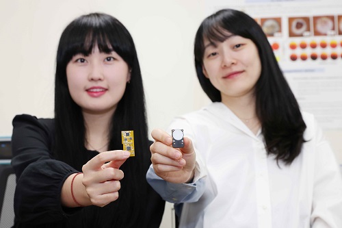 KAIST Succeeds in Real-Time Carbon Dioxide Monitoring Without Batteries or External Power
< (From left) Master's Student Gyurim Jang, Professor Kyeongha Kwon >
KAIST (President Kwang Hyung Lee) announced on June 9th that a research team led by Professor Kyeongha Kwon from the School of Electrical Engineering, in a joint study with Professor Hanjun Ryu's team at Chung-Ang University, has developed a self-powered wireless carbon dioxide (CO2) monitoring system. This innovative system harvests fine vibrational energy from its surroundings to periodically measure CO2 concentrations.
This breakthrough addresses a critical need in environmental monitoring: accurately understanding "how much" CO2 is being emitted to combat climate change and global warming. While CO2 monitoring technology is key to this, existing systems largely rely on batteries or wired power system, imposing limitations on installation and maintenance. The KAIST team tackled this by creating a self-powered wireless system that operates without external power.
The core of this new system is an "Inertia-driven Triboelectric Nanogenerator (TENG)" that converts vibrations (with amplitudes ranging from 20-4000 ㎛ and frequencies from 0-300 Hz) generated by industrial equipment or pipelines into electricity. This enables periodic CO2 concentration measurements and wireless transmission without the need for batteries.
< Figure 1. Concept and configuration of self-powered wireless CO2 monitoring system using fine vibration harvesting (a) System block diagram (b) Photo of fabricated system prototype >
The research team successfully amplified fine vibrations and induced resonance by combining spring-attached 4-stack TENGs. They achieved stable power production of 0.5 mW under conditions of 13 Hz and 0.56 g acceleration. The generated power was then used to operate a CO2 sensor and a Bluetooth Low Energy (BLE) system-on-a-chip (SoC).
Professor Kyeongha Kwon emphasized, "For efficient environmental monitoring, a system that can operate continuously without power limitations is essential." She explained, "In this research, we implemented a self-powered system that can periodically measure and wirelessly transmit CO2 concentrations based on the energy generated from an inertia-driven TENG." She added, "This technology can serve as a foundational technology for future self-powered environmental monitoring platforms integrating various sensors."
< Figure 2. TENG energy harvesting-based wireless CO2 sensing system operation results (c) Experimental setup (d) Measured CO2 concentration results powered by TENG and conventional DC power source >
This research was published on June 1st in the internationally renowned academic journal `Nano Energy (IF 16.8)`. Gyurim Jang, a master's student at KAIST, and Daniel Manaye Tiruneh, a master's student at Chung-Ang University, are the co-first authors of the paper.*Paper Title: Highly compact inertia-driven triboelectric nanogenerator for self-powered wireless CO2 monitoring via fine-vibration harvesting*DOI: 10.1016/j.nanoen.2025.110872
This research was supported by the Saudi Aramco-KAIST CO2 Management Center.
2025.06.09 View 57232
KAIST Succeeds in Real-Time Carbon Dioxide Monitoring Without Batteries or External Power
< (From left) Master's Student Gyurim Jang, Professor Kyeongha Kwon >
KAIST (President Kwang Hyung Lee) announced on June 9th that a research team led by Professor Kyeongha Kwon from the School of Electrical Engineering, in a joint study with Professor Hanjun Ryu's team at Chung-Ang University, has developed a self-powered wireless carbon dioxide (CO2) monitoring system. This innovative system harvests fine vibrational energy from its surroundings to periodically measure CO2 concentrations.
This breakthrough addresses a critical need in environmental monitoring: accurately understanding "how much" CO2 is being emitted to combat climate change and global warming. While CO2 monitoring technology is key to this, existing systems largely rely on batteries or wired power system, imposing limitations on installation and maintenance. The KAIST team tackled this by creating a self-powered wireless system that operates without external power.
The core of this new system is an "Inertia-driven Triboelectric Nanogenerator (TENG)" that converts vibrations (with amplitudes ranging from 20-4000 ㎛ and frequencies from 0-300 Hz) generated by industrial equipment or pipelines into electricity. This enables periodic CO2 concentration measurements and wireless transmission without the need for batteries.
< Figure 1. Concept and configuration of self-powered wireless CO2 monitoring system using fine vibration harvesting (a) System block diagram (b) Photo of fabricated system prototype >
The research team successfully amplified fine vibrations and induced resonance by combining spring-attached 4-stack TENGs. They achieved stable power production of 0.5 mW under conditions of 13 Hz and 0.56 g acceleration. The generated power was then used to operate a CO2 sensor and a Bluetooth Low Energy (BLE) system-on-a-chip (SoC).
Professor Kyeongha Kwon emphasized, "For efficient environmental monitoring, a system that can operate continuously without power limitations is essential." She explained, "In this research, we implemented a self-powered system that can periodically measure and wirelessly transmit CO2 concentrations based on the energy generated from an inertia-driven TENG." She added, "This technology can serve as a foundational technology for future self-powered environmental monitoring platforms integrating various sensors."
< Figure 2. TENG energy harvesting-based wireless CO2 sensing system operation results (c) Experimental setup (d) Measured CO2 concentration results powered by TENG and conventional DC power source >
This research was published on June 1st in the internationally renowned academic journal `Nano Energy (IF 16.8)`. Gyurim Jang, a master's student at KAIST, and Daniel Manaye Tiruneh, a master's student at Chung-Ang University, are the co-first authors of the paper.*Paper Title: Highly compact inertia-driven triboelectric nanogenerator for self-powered wireless CO2 monitoring via fine-vibration harvesting*DOI: 10.1016/j.nanoen.2025.110872
This research was supported by the Saudi Aramco-KAIST CO2 Management Center.
2025.06.09 View 57232 -
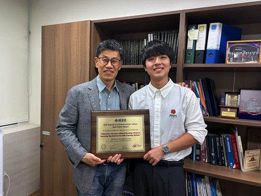 KAIST Professor Jee-Hwan Ryu Receives Global IEEE Robotics Journal Best Paper Award
- Professor Jee-Hwan Ryu of Civil and Environmental Engineering receives the Best Paper Award from the Institute of Electrical and Electronics Engineers (IEEE) Robotics Journal, officially presented at ICRA, a world-renowned robotics conference.
- This is the highest level of international recognition, awarded to only the top 5 papers out of approximately 1,500 published in 2024.
- Securing a new working channel technology for soft growing robots expands the practicality and application possibilities in the field of soft robotics.
< Professor Jee-Hwan Ryu (left), Nam Gyun Kim, Ph.D. Candidate (right) from the KAIST Department of Civil and Environmental Engineering and KAIST Robotics Program >
KAIST (President Kwang-Hyung Lee) announced on the 6th that Professor Jee-Hwan Ryu from the Department of Civil and Environmental Engineering received the 2024 Best Paper Award from the Robotics and Automation Letters (RA-L), a premier journal under the IEEE, at the '2025 IEEE International Conference on Robotics and Automation (ICRA)' held in Atlanta, USA, on May 22nd.
This Best Paper Award is a prestigious honor presented to only the top 5 papers out of approximately 1,500 published in 2024, boasting high international competition and authority.
The award-winning paper by Professor Ryu proposes a novel working channel securing mechanism that significantly expands the practicality and application possibilities of 'Soft Growing Robots,' which are based on soft materials that move or perform tasks through a growing motion similar to plant roots.
< IEEE Robotics Journal Award Ceremony >
Existing soft growing robots move by inflating or contracting their bodies through increasing or decreasing internal pressure, which can lead to blockages in their internal passages. In contrast, the newly developed soft growing robot achieves a growing function while maintaining the internal passage pressure equal to the external atmospheric pressure, thereby successfully securing an internal passage while retaining the robot's flexible and soft characteristics.
This structure allows various materials or tools to be freely delivered through the internal passage (working channel) within the robot and offers the advantage of performing multi-purpose tasks by flexibly replacing equipment according to the working environment.
The research team fabricated a prototype to prove the effectiveness of this technology and verified its performance through various experiments. Specifically, in the slide plate experiment, they confirmed whether materials or equipment could pass through the robot's internal channel without obstruction, and in the pipe pulling experiment, they verified if a long pipe-shaped tool could be pulled through the internal channel.
< Figure 1. Overall hardware structure of the proposed soft growing robot (left) and a cross-sectional view composing the inflatable structure (right) >
Experimental results demonstrated that the internal channel remained stable even while the robot was growing, serving as a key basis for supporting the technology's practicality and scalability.
Professor Jee-Hwan Ryu stated, "This award is very meaningful as it signifies the global recognition of Korea's robotics technology and academic achievements. Especially, it holds great significance in achieving technical progress that can greatly expand the practicality and application fields of soft growing robots. This achievement was possible thanks to the dedication and collaboration of the research team, and I will continue to contribute to the development of robotics technology through innovative research."
< Figure 2. Material supplying mechanism of the Soft Growing Robot >
This research was co-authored by Dongoh Seo, Ph.D. Candidate in Civil and Environmental Engineering, and Nam Gyun Kim, Ph.D. Candidate in Robotics. It was published in IEEE Robotics and Automation Letters on September 1, 2024.
(Paper Title: Inflatable-Structure-Based Working-Channel Securing Mechanism for Soft Growing Robots, DOI: 10.1109/LRA.2024.3426322)
This project was supported simultaneously by the National Research Foundation of Korea's Future Promising Convergence Technology Pioneer Research Project and Mid-career Researcher Project.
2025.06.09 View 11593
KAIST Professor Jee-Hwan Ryu Receives Global IEEE Robotics Journal Best Paper Award
- Professor Jee-Hwan Ryu of Civil and Environmental Engineering receives the Best Paper Award from the Institute of Electrical and Electronics Engineers (IEEE) Robotics Journal, officially presented at ICRA, a world-renowned robotics conference.
- This is the highest level of international recognition, awarded to only the top 5 papers out of approximately 1,500 published in 2024.
- Securing a new working channel technology for soft growing robots expands the practicality and application possibilities in the field of soft robotics.
< Professor Jee-Hwan Ryu (left), Nam Gyun Kim, Ph.D. Candidate (right) from the KAIST Department of Civil and Environmental Engineering and KAIST Robotics Program >
KAIST (President Kwang-Hyung Lee) announced on the 6th that Professor Jee-Hwan Ryu from the Department of Civil and Environmental Engineering received the 2024 Best Paper Award from the Robotics and Automation Letters (RA-L), a premier journal under the IEEE, at the '2025 IEEE International Conference on Robotics and Automation (ICRA)' held in Atlanta, USA, on May 22nd.
This Best Paper Award is a prestigious honor presented to only the top 5 papers out of approximately 1,500 published in 2024, boasting high international competition and authority.
The award-winning paper by Professor Ryu proposes a novel working channel securing mechanism that significantly expands the practicality and application possibilities of 'Soft Growing Robots,' which are based on soft materials that move or perform tasks through a growing motion similar to plant roots.
< IEEE Robotics Journal Award Ceremony >
Existing soft growing robots move by inflating or contracting their bodies through increasing or decreasing internal pressure, which can lead to blockages in their internal passages. In contrast, the newly developed soft growing robot achieves a growing function while maintaining the internal passage pressure equal to the external atmospheric pressure, thereby successfully securing an internal passage while retaining the robot's flexible and soft characteristics.
This structure allows various materials or tools to be freely delivered through the internal passage (working channel) within the robot and offers the advantage of performing multi-purpose tasks by flexibly replacing equipment according to the working environment.
The research team fabricated a prototype to prove the effectiveness of this technology and verified its performance through various experiments. Specifically, in the slide plate experiment, they confirmed whether materials or equipment could pass through the robot's internal channel without obstruction, and in the pipe pulling experiment, they verified if a long pipe-shaped tool could be pulled through the internal channel.
< Figure 1. Overall hardware structure of the proposed soft growing robot (left) and a cross-sectional view composing the inflatable structure (right) >
Experimental results demonstrated that the internal channel remained stable even while the robot was growing, serving as a key basis for supporting the technology's practicality and scalability.
Professor Jee-Hwan Ryu stated, "This award is very meaningful as it signifies the global recognition of Korea's robotics technology and academic achievements. Especially, it holds great significance in achieving technical progress that can greatly expand the practicality and application fields of soft growing robots. This achievement was possible thanks to the dedication and collaboration of the research team, and I will continue to contribute to the development of robotics technology through innovative research."
< Figure 2. Material supplying mechanism of the Soft Growing Robot >
This research was co-authored by Dongoh Seo, Ph.D. Candidate in Civil and Environmental Engineering, and Nam Gyun Kim, Ph.D. Candidate in Robotics. It was published in IEEE Robotics and Automation Letters on September 1, 2024.
(Paper Title: Inflatable-Structure-Based Working-Channel Securing Mechanism for Soft Growing Robots, DOI: 10.1109/LRA.2024.3426322)
This project was supported simultaneously by the National Research Foundation of Korea's Future Promising Convergence Technology Pioneer Research Project and Mid-career Researcher Project.
2025.06.09 View 11593 -
 KAIST Innovates Mid-Infrared Photodetectors for Exoplanet Detection, Expanding Applications to Environmental and Medical Fields
NASA’s James Webb Space Telescope (JWST) utilizes mid-infrared spectroscopy to precisely analyze molecular components such as water vapor and sulfur dioxide in exoplanet atmospheres. The key to this analysis, where each molecule exhibits a unique spectral "fingerprint," lies in highly sensitive photodetector technology capable of measuring extremely weak light intensities. Recently, KAIST researchers have developed an innovative photodetector capable of detecting a broad range of mid-infrared spectra, garnering significant attention.
< Photo 1. (from the left) Ph.D. candidate Inki Kim (co-author), Professor SangHyeon Kim (corresponding author), Dr. Joonsup Shim (first author), and Dr. Jinha Lim (co-author) of KAIST School of Electrical Engineering. >
KAIST (represented by President Kwang-Hyung Lee) announced on the 27th of March that a research team led by Professor SangHyeon Kim from the School of Electrical Engineering has developed a mid-infrared photodetector that operates stably at room temperature, marking a major turning point for the commercialization of ultra-compact optical sensors.
The newly developed photodetector utilizes conventional silicon-based CMOS processes, enabling low-cost mass production while maintaining stable operation at room temperature. Notably, the research team successfully demonstrated the real-time detection of carbon dioxide (CO₂) gas using ultra-compact and ultra-thin optical sensors equipped with this photodetector, proving its potential for environmental monitoring and hazardous gas analysis.
Existing mid-infrared photodetectors generally require cooling systems due to high thermal noise at room temperature. These cooling systems increase the size and cost of equipment, making miniaturization and integration into portable devices challenging. Furthermore, conventional mid-infrared photodetectors are incompatible with silicon-based CMOS processes, limiting large-scale production and commercialization.
To address these limitations, the research team developed a waveguide-integrated photodetector using germanium (Ge), a Group IV element like silicon. This approach enables broad-spectrum mid-infrared detection while ensuring stable operation at room temperature.
< Figure 1. Schematic diagram of a room-temperature mid-infrared waveguide-integrated photodetector based on the Ge-on-insulator optical platform proposed in this study (top). Optical microscope image of the integrated photodetector connected with the sensing unit (bottom). >
A waveguide is a structure designed to efficiently guide light along a specific path with minimal loss. To implement various optical functions on a chip (on-chip), the development of waveguide-integrated photodetectors and waveguide-based optical components is essential.
Unlike conventional photodetectors that primarily rely on bandgap absorption principles, this new technology leverages the bolometric effect*, allowing it to detect the entire mid-infrared spectral range. As a result, it can be widely applied to the real-time sensing of various molecular species.
*Bolometric effect: A principle in which light absorption leads to an increase in temperature, causing electrical signals to change accordingly.
The waveguide-integrated mid-infrared photodetector developed by the research team is considered a groundbreaking innovation that overcomes the limitations of existing mid-infrared sensor technologies, including the need for cooling, difficulties in mass production, and high costs.
< Figure 2. Room temperature photoresponse characteristics of the mid-infrared waveguide photodetector proposed in this study (left) and real-time carbon dioxide (CO2) gas sensing results using the photodetector (right). >
This breakthrough technology is expected to be applicable across diverse fields, including environmental monitoring, medical diagnostics, industrial process management, national defense and security, and smart devices. It also paves the way for next-generation mid-infrared sensor advancements.
Professor SangHyeon Kim from KAIST stated, "This research represents a novel approach that overcomes the limitations of existing mid-infrared photodetector technologies and has great potential for practical applications in various fields." He further emphasized, "Since this sensor technology is compatible with CMOS processes, it enables low-cost mass production, making it highly suitable for next-generation environmental monitoring systems and smart manufacturing sites."
< Figure 3. Performance comparison image of a room-temperature mid-infrared waveguide photodetector fabricated with the technology proposed in this study. It achieves the world’s highest performance compared to existing technologies utilizing the Bolometric effect, and is the only solution compatible with CMOS processes. The technology proposed by our research team is characterized by its ability to respond to a wide spectrum of the mid-infrared band without limitations. >
The study, with Dr. Joonsup Shim (currently a postdoctoral researcher at Harvard University) as the first author, was published on March 19, 2025 in the internationally renowned journal Light: Science & Applications (JCR 2.9%, IF=20.6).
(Paper title: “Room-temperature waveguide-integrated photodetector using bolometric effect for mid-infrared spectroscopy applications,” https://doi.org/10.1038/s41377-025-01803-3)
2025.03.27 View 9788
KAIST Innovates Mid-Infrared Photodetectors for Exoplanet Detection, Expanding Applications to Environmental and Medical Fields
NASA’s James Webb Space Telescope (JWST) utilizes mid-infrared spectroscopy to precisely analyze molecular components such as water vapor and sulfur dioxide in exoplanet atmospheres. The key to this analysis, where each molecule exhibits a unique spectral "fingerprint," lies in highly sensitive photodetector technology capable of measuring extremely weak light intensities. Recently, KAIST researchers have developed an innovative photodetector capable of detecting a broad range of mid-infrared spectra, garnering significant attention.
< Photo 1. (from the left) Ph.D. candidate Inki Kim (co-author), Professor SangHyeon Kim (corresponding author), Dr. Joonsup Shim (first author), and Dr. Jinha Lim (co-author) of KAIST School of Electrical Engineering. >
KAIST (represented by President Kwang-Hyung Lee) announced on the 27th of March that a research team led by Professor SangHyeon Kim from the School of Electrical Engineering has developed a mid-infrared photodetector that operates stably at room temperature, marking a major turning point for the commercialization of ultra-compact optical sensors.
The newly developed photodetector utilizes conventional silicon-based CMOS processes, enabling low-cost mass production while maintaining stable operation at room temperature. Notably, the research team successfully demonstrated the real-time detection of carbon dioxide (CO₂) gas using ultra-compact and ultra-thin optical sensors equipped with this photodetector, proving its potential for environmental monitoring and hazardous gas analysis.
Existing mid-infrared photodetectors generally require cooling systems due to high thermal noise at room temperature. These cooling systems increase the size and cost of equipment, making miniaturization and integration into portable devices challenging. Furthermore, conventional mid-infrared photodetectors are incompatible with silicon-based CMOS processes, limiting large-scale production and commercialization.
To address these limitations, the research team developed a waveguide-integrated photodetector using germanium (Ge), a Group IV element like silicon. This approach enables broad-spectrum mid-infrared detection while ensuring stable operation at room temperature.
< Figure 1. Schematic diagram of a room-temperature mid-infrared waveguide-integrated photodetector based on the Ge-on-insulator optical platform proposed in this study (top). Optical microscope image of the integrated photodetector connected with the sensing unit (bottom). >
A waveguide is a structure designed to efficiently guide light along a specific path with minimal loss. To implement various optical functions on a chip (on-chip), the development of waveguide-integrated photodetectors and waveguide-based optical components is essential.
Unlike conventional photodetectors that primarily rely on bandgap absorption principles, this new technology leverages the bolometric effect*, allowing it to detect the entire mid-infrared spectral range. As a result, it can be widely applied to the real-time sensing of various molecular species.
*Bolometric effect: A principle in which light absorption leads to an increase in temperature, causing electrical signals to change accordingly.
The waveguide-integrated mid-infrared photodetector developed by the research team is considered a groundbreaking innovation that overcomes the limitations of existing mid-infrared sensor technologies, including the need for cooling, difficulties in mass production, and high costs.
< Figure 2. Room temperature photoresponse characteristics of the mid-infrared waveguide photodetector proposed in this study (left) and real-time carbon dioxide (CO2) gas sensing results using the photodetector (right). >
This breakthrough technology is expected to be applicable across diverse fields, including environmental monitoring, medical diagnostics, industrial process management, national defense and security, and smart devices. It also paves the way for next-generation mid-infrared sensor advancements.
Professor SangHyeon Kim from KAIST stated, "This research represents a novel approach that overcomes the limitations of existing mid-infrared photodetector technologies and has great potential for practical applications in various fields." He further emphasized, "Since this sensor technology is compatible with CMOS processes, it enables low-cost mass production, making it highly suitable for next-generation environmental monitoring systems and smart manufacturing sites."
< Figure 3. Performance comparison image of a room-temperature mid-infrared waveguide photodetector fabricated with the technology proposed in this study. It achieves the world’s highest performance compared to existing technologies utilizing the Bolometric effect, and is the only solution compatible with CMOS processes. The technology proposed by our research team is characterized by its ability to respond to a wide spectrum of the mid-infrared band without limitations. >
The study, with Dr. Joonsup Shim (currently a postdoctoral researcher at Harvard University) as the first author, was published on March 19, 2025 in the internationally renowned journal Light: Science & Applications (JCR 2.9%, IF=20.6).
(Paper title: “Room-temperature waveguide-integrated photodetector using bolometric effect for mid-infrared spectroscopy applications,” https://doi.org/10.1038/s41377-025-01803-3)
2025.03.27 View 9788