%4b%69%62%75%6d%20%4b%61%6e%67
-
 KAIST Controls Where 2D Semiconductor Crystals Begin to Grow, Addressing a Key Challenge in Stacking AI Chips
Two-dimensional (2D) semiconductors, only a few atomic layers thick, are a promising material for making AI chips faster and more energy efficient by stacking additional semiconductor layers on top of existing computing circuits. However, when crystals form at multiple random locations during growth, it is difficult to produce high-quality semiconductors at the desired positions. A KAIST joint research team has developed a technology that sets in advance where a crystal begins to grow and allows only one crystal to grow at that position. By controlling the starting point of semiconductor growth, the work addresses a key challenge in realizing next-generation stacked semiconductors.
KAIST announced that a research team led by Professor Kibum Kang from the Department of Materials Science and Engineering, in collaboration with UNIST, Hanyang University, and TDS Innovation (Co-CEOs Kibum Kang and Sanghyun Mo), has developed a new growth technique that precisely controls the location of nucleation, the stage at which 2D semiconductor crystals first form, using chemical species released from an oxide barrier.
When AI generates responses or processes large amounts of data, time and power are consumed not only by computation but also by moving data within the chip. Stacking the devices used for computation and data storage vertically, so that they are placed close together, shortens the distance that data must travel and can reduce processing delays and power consumption. This requires a technology that forms high-quality semiconductors directly at the required positions on top of circuits that have already been fabricated.
Deposited semiconductors, in which devices are made by forming a thin film of semiconductor material directly on the required surface, are a promising technology for building stacked chips. 2D semiconductors are particularly well suited for stacking thin device layers because they retain the electrical properties of a semiconductor while being only a few atomic layers thick.
The challenge is that, as a thin semiconductor film grows, the positions where crystals begin to form are inherently random. A crystal is a structure in which the atoms that make up the semiconductor are arranged in a regular, repeating pattern. When crystals grow separately from several locations and meet, grain boundaries form between them. These boundaries hinder the movement of electrons and can degrade the quality of the semiconductor.
Area-selective growth techniques, which define in advance the regions where a semiconductor will grow, already existed. However, it has been difficult to control exactly where crystals first form within those regions and how many of them form. The research team achieved deterministic nucleation, in which nucleation that previously occurred at random takes place one at a time at defined positions. In addition to defining the region where the semiconductor will grow, the team also determined the point within that region where growth begins.
The researchers named the technique etching-flux-mediated single-centered nucleation (EF-SCN). The key element is oxygen released from an oxide barrier, such as hafnium oxide (HfO₂), that surrounds the growth region. This oxygen acts as an etching flux that suppresses the formation of crystal nuclei of molybdenum disulfide (MoS₂), a representative 2D semiconductor. Etching refers to chemically removing material, and flux refers to the flow of a specific chemical species that is transported and supplied in a way that affects nearby chemical reactions.
The suppressing effect is strong at the edges near the oxide barrier and becomes weaker toward the center, which is farthest from the barrier. Using this difference, the team caused a single crystal to begin growing at only one point in the center. While the crystal that started at the center continued to grow, the formation of new crystals around it was also suppressed, so that the single crystal could grow larger.
In experiments, the team grew one MoS₂ single crystal at a designated central position in more than 99% of 400 different patterns. A single crystal has one continuous atomic arrangement, and because it reduces the boundaries that form where multiple crystals meet, it is advantageous for producing high-quality semiconductors. Using MoS₂–MoSe₂ lateral heterostructures grown with this method, the team also deposited a thin film of ruthenium (Ru) metal selectively on the molybdenum diselenide (MoSe₂) regions only. The researchers further analyzed the principle behind this position control through growth experiments and simulations.
The significance of this work is that it turns the starting point of semiconductor thin-film growth, which had been determined at random, into a process parameter that can be designed. Instead of fabricating 2D semiconductors elsewhere and then transferring them, this approach could lead to a manufacturing technology that grows high-quality semiconductors directly at the required positions on a chip. Deposited semiconductors are expected to be adopted in the 2030s to improve the performance and lower the power consumption of AI chips. If applied to stacked AI chips, the technology could reduce the time and energy spent on moving data, which would shorten the time users wait for AI responses and reduce the power demands of data centers.
“In thin-film growth, where a crystal forms is inherently a matter of probability, and the key significance of this study is that it allows that starting point to be determined at a desired position,” said Professor Kibum Kang. Professor Kang added that the technology will serve as the basis for stacked-channel processes, in which semiconductor devices are stacked vertically, by growing high-quality 2D semiconductors directly where they are needed.
“In 2D semiconductors, the position where growth begins can change in response to even small chemical changes in the surroundings,” said Dr. Jeongwon Park, a co-first author. Park explained that the significance of the study lies in using this property to control where the semiconductor begins to grow.
Dr. Park and master’s student Jiyun Kim from the KAIST Department of Materials Science and Engineering, Sumin Kang, who received a master’s degree from the same department, integrated M.S.–Ph.D. student Jieun Oh from the Department of Materials Science and Chemical Engineering at Hanyang University, and integrated M.S.–Ph.D. student Youngmin Sunwoo from the Graduate School of Semiconductor Materials and Devices Engineering at UNIST participated as co-first authors. The findings were published in Nature on October 8.
Paper title: Spatially deterministic nucleation of 2D semiconductors by etching flux
DOI: 10.1038/s41586-026-11095-1
This research was supported by the Nano and Material Technology Development Program and the Basic Science Research Program of the National Research Foundation of Korea (NRF), funded by the Ministry of Science and ICT (MSIT). Additional support was provided by the International Cooperation Program for Source Technology Development, the Development of vdW Materials and Process Technologies for Ultra-High-Density Semiconductors Program, the Next-Generation Intelligent Semiconductor Technology Development Program, the Ministry of Trade, Industry and Energy (MOTIE), the Korea Institute for Advancement of Technology (KIAT), the Commercialization Promotion Agency for R&D Outcomes (COMPA), the Innopolis Foundation, the Ministry of SMEs and Startups (MSS), and NVIDIA.
2026.10.13 View 236
-
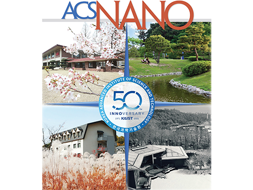 ACS Nano Special Edition Highlights Innovations at KAIST
- The collective intelligence and technological innovation of KAIST was highlighted with case studies including the Post-COVID-19 New Deal R&D Initiative Project. -
KAIST’s innovative academic achievements and R&D efforts for addressing the world’s greatest challenges such as the COVID-19 pandemic were featured in ACS Nano as part of its special virtual issue commemorating the 50th anniversary of KAIST. The issue consisted of 14 review articles contributed by KAIST faculty from five departments, including two from Professor Il-Doo Kim from the Department of Materials Science and Engineering, who serves as an associate editor of the ACS Nano.
ACS Nano, the leading international journal in nanoscience and nanotechnology, published a special virtual issue last month, titled ‘Celebrating 50 Years of KAIST: Collective Intelligence and Innovation for Confronting Contemporary Issues.’
This special virtual issue introduced KAIST’s vision of becoming a ‘global value-creative leading university’ and its progress toward this vision over the last 50 years. The issue explained how KAIST has served as the main hub for advanced scientific research and technological innovation in South Korea since its establishment in 1971, and how its faculty and over 69,000 graduates played a key role in propelling the nation’s rapid industrialization and economic development.
The issue also emphasized the need for KAIST to enhance global cooperation and the exchange of ideas in the years to come, especially during the post-COVID era intertwined with the Fourth Industrial Revolution (4IR). In this regard, the issue cited the first ‘KAIST Emerging Materials e-Symposium (EMS)’, which was held online for five days in September of last year with a global audience of over 10,000 participating live via Zoom and YouTube, as a successful example of what academic collaboration could look like in the post-COVID and 4IR eras.
In addition, the “Science & Technology New Deal Project for COVID-19 Response,” a project conducted by KAIST with support from the Ministry of Science and ICT (MSIT) of South Korea, was also introduced as another excellent case of KAIST’s collective intelligence and technological innovation. The issue highlighted some key achievements from this project for overcoming the pandemic-driven crisis, such as: reusable anti-virus filters, negative-pressure ambulances for integrated patient transport and hospitalization, and movable and expandable negative-pressure ward modules.
“We hold our expectations high for the outstanding achievements and progress KAIST will have made by its centennial,” said Professor Kim on the background of curating the 14 review articles contributed by KAIST faculty from the fields of Materials Science and Engineering (MSE), Chemical and Biomolecular Engineering (CBE), Nuclear and Quantum Engineering (NQE), Electrical Engineering (EE), and Chemistry (Chem).
Review articles discussing emerging materials and their properties covered photonic carbon dots (Professor Chan Beum Park, MSE), single-atom and ensemble catalysts (Professor Hyunjoo Lee, CBE), and metal/metal oxide electrocatalysts (Professor Sung-Yoon Chung, MSE).
Review articles discussing materials processing covered 2D layered materials synthesis based on interlayer engineering (Professor Kibum Kang, MSE), eco-friendly methods for solar cell production (Professor Bumjoon J. Kim, CBE), an ex-solution process for the synthesis of highly stable catalysts (Professor WooChul Jung, MSE), and 3D light-patterning synthesis of ordered nanostructures (Professor Seokwoo Jeon, MSE, and Professor Dongchan Jang, NQE).
Review articles discussing advanced analysis techniques covered operando materials analyses (Professor Jeong Yeong Park, Chem), graphene liquid cell transmission electron microscopy (Professor Jong Min Yuk, MSE), and multiscale modeling and visualization of materials systems (Professor Seungbum Hong, MSE).
Review articles discussing practical state-of-the-art devices covered chemiresistive hydrogen sensors (Professor Il-Doo Kim, MSE), patient-friendly diagnostics and implantable treatment devices (Professor Steve Park, MSE), triboelectric nanogenerators (Professor Yang-Kyu Choi, EE), and next-generation lithium-air batteries (Professor Hye Ryung Byon, Chem, and Professor Il-Doo Kim, MSE).
In addition to Professor Il-Doo Kim, post-doctoral researcher Dr. Jaewan Ahn from the KAIST Applied Science Research Institute, Dean of the College of Engineering at KAIST Professor Choongsik Bae, and ACS Nano Editor-in-Chief Professor Paul S. Weiss from the University of California, Los Angeles also contributed to the publication of this ACS Nano special virtual issue.
The issue can be viewed and downloaded from the ACS Nano website at https://doi.org/10.1021/acsnano.1c01101.
Image credit: KAIST
Image usage restrictions: News organizations may use or redistribute this image,with proper attribution, as part of news coverage of this paper only.
Publication:
Ahn, J., et al. (2021) Celebrating 50 Years of KAIST: Collective Intelligence and Innovation for Confronting Contemporary Issues. ACS Nano 15(3): 1895-1907. Available online at https://doi.org/10.1021/acsnano.1c01101
Profile:
Il-Doo Kim, Ph.D
Chair Professor
idkim@kaist.ac.kr
http://advnano.kaist.ac.kr
Advanced Nanomaterials and Energy Lab.
Department of Materials Science and Engineering
Membrane Innovation Center for Anti-Virus and Air-Quality Control
https://kaist.ac.kr/
Korea Advanced Institute of Science and Technology (KAIST) Daejeon, Republic of Korea
(END)
2021.03.05 View 54920