Yang-Kyu+Choi
-
 The World’s First Hacking-preventing Cryptographic Semiconductor Chip
With the dramatic increase in the amount of information exchanged between components or devices in the 5G/6G era, such as for the Internet of Things (IoT) and autonomous driving, hacking attacks are becoming more sophisticated. Consequently, enhancing security functions is essential for safely transmitting data between and among devices.
On February 29th, a KAIST research team led by Professors Yang-gyu Choi and Seung-tak Ryu from the School of Electrical Engineering announced the successful development of the world's first security cryptographic semiconductor.
The team has developed the Cryptoristor, a cryptographic transistor based on FinFET technology, produced through a 100% silicon-compatible process, for the first time in the world. Cryptoristor is a random number generator (RNG) with unparalleled characteristics, featuring a unique structure comprising a single transistor and a distinctive mechanism.
In all security environments, including artificial intelligence, the most crucial element is the RNG. In the most commonly used security chip, the Advanced Encryption Standard (AES), the RNG is a core component, occupying approximately 75% of the total chip area and more than 85% of its energy consumption. Hence, there is an urgent need for the development of low-power/ultra-small RNGs suitable for mobile or IoT devices.
Existing RNGs come with limitations as they lack compatibility with silicon CMOS processes and circuit-based RNGs occupy a large surface area.
In contrast, the team’s newly developed Cryptoristor, a cryptographic semiconductor based on a single-component structure, consumes and occupies less than .001 of the power and area compared to the current chips being used. Utilizing the inherent randomness of FinFETs, fabricated on a Silicon-on-Insulator (SOI) substrate with an insulating layer formed beneath the silicon, the team developed an RNG that unpredictably produces zeroes and ones.
< Figure 1. Conceptual diagram of the security cryptographic transistor device. >
Generally speaking, preventing hackers from predicting the encrypted algorithms during data exchanges through mobile devices is pivotal. Therefore, this method ensures unpredictability by generating random sequences of zeroes and ones that change every time.
Moreover, while the Cryptoristor-based RNG research is the world's first of its kind without any international implementation cases, it shares the same transistor structure as existing logic or memory components. This enables 100% production through rapid mass production processes using existing semiconductor facilities at a low cost.
Seung-il Kim, a PhD student who led the research, explained the significance of the study, stating, "As a cryptographic semiconductor, the ultra-small/low-power random number generator enhances security through its distinctive unpredictability, supporting safe hyperconnectivity with secure transmissions between chips or devices. Particularly, compared to previous research, it offers excellent advantages in terms of energy consumption, integration density, and cost, making it suitable for IoT device environments."
This research, with master’s student Hyung-jin Yoo as the co-author, was officially published in the online edition of Science Advances, a sister journal of Science, in February 2024 (research paper title: Cryptographic transistor for true random number generator with low power consumption).
This research received support from the Next-Generation Intelligent Semiconductor Technology Development Project and the Core Technology Development Project for the National Semiconductor Research Laboratory.
2024.03.07 View 6641
The World’s First Hacking-preventing Cryptographic Semiconductor Chip
With the dramatic increase in the amount of information exchanged between components or devices in the 5G/6G era, such as for the Internet of Things (IoT) and autonomous driving, hacking attacks are becoming more sophisticated. Consequently, enhancing security functions is essential for safely transmitting data between and among devices.
On February 29th, a KAIST research team led by Professors Yang-gyu Choi and Seung-tak Ryu from the School of Electrical Engineering announced the successful development of the world's first security cryptographic semiconductor.
The team has developed the Cryptoristor, a cryptographic transistor based on FinFET technology, produced through a 100% silicon-compatible process, for the first time in the world. Cryptoristor is a random number generator (RNG) with unparalleled characteristics, featuring a unique structure comprising a single transistor and a distinctive mechanism.
In all security environments, including artificial intelligence, the most crucial element is the RNG. In the most commonly used security chip, the Advanced Encryption Standard (AES), the RNG is a core component, occupying approximately 75% of the total chip area and more than 85% of its energy consumption. Hence, there is an urgent need for the development of low-power/ultra-small RNGs suitable for mobile or IoT devices.
Existing RNGs come with limitations as they lack compatibility with silicon CMOS processes and circuit-based RNGs occupy a large surface area.
In contrast, the team’s newly developed Cryptoristor, a cryptographic semiconductor based on a single-component structure, consumes and occupies less than .001 of the power and area compared to the current chips being used. Utilizing the inherent randomness of FinFETs, fabricated on a Silicon-on-Insulator (SOI) substrate with an insulating layer formed beneath the silicon, the team developed an RNG that unpredictably produces zeroes and ones.
< Figure 1. Conceptual diagram of the security cryptographic transistor device. >
Generally speaking, preventing hackers from predicting the encrypted algorithms during data exchanges through mobile devices is pivotal. Therefore, this method ensures unpredictability by generating random sequences of zeroes and ones that change every time.
Moreover, while the Cryptoristor-based RNG research is the world's first of its kind without any international implementation cases, it shares the same transistor structure as existing logic or memory components. This enables 100% production through rapid mass production processes using existing semiconductor facilities at a low cost.
Seung-il Kim, a PhD student who led the research, explained the significance of the study, stating, "As a cryptographic semiconductor, the ultra-small/low-power random number generator enhances security through its distinctive unpredictability, supporting safe hyperconnectivity with secure transmissions between chips or devices. Particularly, compared to previous research, it offers excellent advantages in terms of energy consumption, integration density, and cost, making it suitable for IoT device environments."
This research, with master’s student Hyung-jin Yoo as the co-author, was officially published in the online edition of Science Advances, a sister journal of Science, in February 2024 (research paper title: Cryptographic transistor for true random number generator with low power consumption).
This research received support from the Next-Generation Intelligent Semiconductor Technology Development Project and the Core Technology Development Project for the National Semiconductor Research Laboratory.
2024.03.07 View 6641 -
 Brain-Inspired Highly Scalable Neuromorphic Hardware Presented
Neurons and synapses based on single transistor can dramatically reduce the hardware cost and accelerate the commercialization of neuromorphic hardware
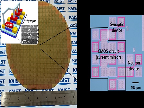
KAIST researchers fabricated a brain-inspired highly scalable neuromorphic hardware by co-integrating single transistor neurons and synapses. Using standard silicon complementary metal-oxide-semiconductor (CMOS) technology, the neuromorphic hardware is expected to reduce chip cost and simplify fabrication procedures.
The research team led by Yang-Kyu Choi and Sung-Yool Choi produced a neurons and synapses based on single transistor for highly scalable neuromorphic hardware and showed the ability to recognize text and face images. This research was featured in Science Advances on August 4.
Neuromorphic hardware has attracted a great deal of attention because of its artificial intelligence functions, but consuming ultra-low power of less than 20 watts by mimicking the human brain. To make neuromorphic hardware work, a neuron that generates a spike when integrating a certain signal, and a synapse remembering the connection between two neurons are necessary, just like the biological brain. However, since neurons and synapses constructed on digital or analog circuits occupy a large space, there is a limit in terms of hardware efficiency and costs. Since the human brain consists of about 1011 neurons and 1014 synapses, it is necessary to improve the hardware cost in order to apply it to mobile and IoT devices.
To solve the problem, the research team mimicked the behavior of biological neurons and synapses with a single transistor, and co-integrated them onto an 8-inch wafer. The manufactured neuromorphic transistors have the same structure as the transistors for memory and logic that are currently mass-produced. In addition, the neuromorphic transistors proved for the first time that they can be implemented with a ‘Janus structure’ that functions as both neuron and synapse, just like coins have heads and tails.
Professor Yang-Kyu Choi said that this work can dramatically reduce the hardware cost by replacing the neurons and synapses that were based on complex digital and analog circuits with a single transistor. "We have demonstrated that neurons and synapses can be implemented using a single transistor," said Joon-Kyu Han, the first author. "By co-integrating single transistor neurons and synapses on the same wafer using a standard CMOS process, the hardware cost of the neuromorphic hardware has been improved, which will accelerate the commercialization of neuromorphic hardware,” Han added.This research was supported by the National Research Foundation (NRF) and IC Design Education Center (IDEC).
-PublicationJoon-Kyu Han, Sung-Yool Choi, Yang-Kyu Choi, et al.“Cointegration of single-transistor neurons and synapses by nanoscale CMOS fabrication for highly scalable neuromorphic hardware,” Science Advances (DOI: 10.1126/sciadv.abg8836)
-ProfileProfessor Yang-Kyu ChoiNano-Oriented Bio-Electronics Labhttps://sites.google.com/view/nobelab/
School of Electrical EngineeringKAIST
Professor Sung-Yool ChoiMolecular and Nano Device Laboratoryhttps://www.mndl.kaist.ac.kr/
School of Electrical EngineeringKAIST
2021.08.05 View 10684
Brain-Inspired Highly Scalable Neuromorphic Hardware Presented
Neurons and synapses based on single transistor can dramatically reduce the hardware cost and accelerate the commercialization of neuromorphic hardware
KAIST researchers fabricated a brain-inspired highly scalable neuromorphic hardware by co-integrating single transistor neurons and synapses. Using standard silicon complementary metal-oxide-semiconductor (CMOS) technology, the neuromorphic hardware is expected to reduce chip cost and simplify fabrication procedures.
The research team led by Yang-Kyu Choi and Sung-Yool Choi produced a neurons and synapses based on single transistor for highly scalable neuromorphic hardware and showed the ability to recognize text and face images. This research was featured in Science Advances on August 4.
Neuromorphic hardware has attracted a great deal of attention because of its artificial intelligence functions, but consuming ultra-low power of less than 20 watts by mimicking the human brain. To make neuromorphic hardware work, a neuron that generates a spike when integrating a certain signal, and a synapse remembering the connection between two neurons are necessary, just like the biological brain. However, since neurons and synapses constructed on digital or analog circuits occupy a large space, there is a limit in terms of hardware efficiency and costs. Since the human brain consists of about 1011 neurons and 1014 synapses, it is necessary to improve the hardware cost in order to apply it to mobile and IoT devices.
To solve the problem, the research team mimicked the behavior of biological neurons and synapses with a single transistor, and co-integrated them onto an 8-inch wafer. The manufactured neuromorphic transistors have the same structure as the transistors for memory and logic that are currently mass-produced. In addition, the neuromorphic transistors proved for the first time that they can be implemented with a ‘Janus structure’ that functions as both neuron and synapse, just like coins have heads and tails.
Professor Yang-Kyu Choi said that this work can dramatically reduce the hardware cost by replacing the neurons and synapses that were based on complex digital and analog circuits with a single transistor. "We have demonstrated that neurons and synapses can be implemented using a single transistor," said Joon-Kyu Han, the first author. "By co-integrating single transistor neurons and synapses on the same wafer using a standard CMOS process, the hardware cost of the neuromorphic hardware has been improved, which will accelerate the commercialization of neuromorphic hardware,” Han added.This research was supported by the National Research Foundation (NRF) and IC Design Education Center (IDEC).
-PublicationJoon-Kyu Han, Sung-Yool Choi, Yang-Kyu Choi, et al.“Cointegration of single-transistor neurons and synapses by nanoscale CMOS fabrication for highly scalable neuromorphic hardware,” Science Advances (DOI: 10.1126/sciadv.abg8836)
-ProfileProfessor Yang-Kyu ChoiNano-Oriented Bio-Electronics Labhttps://sites.google.com/view/nobelab/
School of Electrical EngineeringKAIST
Professor Sung-Yool ChoiMolecular and Nano Device Laboratoryhttps://www.mndl.kaist.ac.kr/
School of Electrical EngineeringKAIST
2021.08.05 View 10684 -
 ACS Nano Special Edition Highlights Innovations at KAIST
- The collective intelligence and technological innovation of KAIST was highlighted with case studies including the Post-COVID-19 New Deal R&D Initiative Project. -
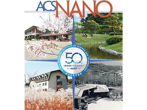
KAIST’s innovative academic achievements and R&D efforts for addressing the world’s greatest challenges such as the COVID-19 pandemic were featured in ACS Nano as part of its special virtual issue commemorating the 50th anniversary of KAIST. The issue consisted of 14 review articles contributed by KAIST faculty from five departments, including two from Professor Il-Doo Kim from the Department of Materials Science and Engineering, who serves as an associate editor of the ACS Nano.
ACS Nano, the leading international journal in nanoscience and nanotechnology, published a special virtual issue last month, titled ‘Celebrating 50 Years of KAIST: Collective Intelligence and Innovation for Confronting Contemporary Issues.’
This special virtual issue introduced KAIST’s vision of becoming a ‘global value-creative leading university’ and its progress toward this vision over the last 50 years. The issue explained how KAIST has served as the main hub for advanced scientific research and technological innovation in South Korea since its establishment in 1971, and how its faculty and over 69,000 graduates played a key role in propelling the nation’s rapid industrialization and economic development.
The issue also emphasized the need for KAIST to enhance global cooperation and the exchange of ideas in the years to come, especially during the post-COVID era intertwined with the Fourth Industrial Revolution (4IR). In this regard, the issue cited the first ‘KAIST Emerging Materials e-Symposium (EMS)’, which was held online for five days in September of last year with a global audience of over 10,000 participating live via Zoom and YouTube, as a successful example of what academic collaboration could look like in the post-COVID and 4IR eras.
In addition, the “Science & Technology New Deal Project for COVID-19 Response,” a project conducted by KAIST with support from the Ministry of Science and ICT (MSIT) of South Korea, was also introduced as another excellent case of KAIST’s collective intelligence and technological innovation. The issue highlighted some key achievements from this project for overcoming the pandemic-driven crisis, such as: reusable anti-virus filters, negative-pressure ambulances for integrated patient transport and hospitalization, and movable and expandable negative-pressure ward modules.
“We hold our expectations high for the outstanding achievements and progress KAIST will have made by its centennial,” said Professor Kim on the background of curating the 14 review articles contributed by KAIST faculty from the fields of Materials Science and Engineering (MSE), Chemical and Biomolecular Engineering (CBE), Nuclear and Quantum Engineering (NQE), Electrical Engineering (EE), and Chemistry (Chem).
Review articles discussing emerging materials and their properties covered photonic carbon dots (Professor Chan Beum Park, MSE), single-atom and ensemble catalysts (Professor Hyunjoo Lee, CBE), and metal/metal oxide electrocatalysts (Professor Sung-Yoon Chung, MSE).
Review articles discussing materials processing covered 2D layered materials synthesis based on interlayer engineering (Professor Kibum Kang, MSE), eco-friendly methods for solar cell production (Professor Bumjoon J. Kim, CBE), an ex-solution process for the synthesis of highly stable catalysts (Professor WooChul Jung, MSE), and 3D light-patterning synthesis of ordered nanostructures (Professor Seokwoo Jeon, MSE, and Professor Dongchan Jang, NQE).
Review articles discussing advanced analysis techniques covered operando materials analyses (Professor Jeong Yeong Park, Chem), graphene liquid cell transmission electron microscopy (Professor Jong Min Yuk, MSE), and multiscale modeling and visualization of materials systems (Professor Seungbum Hong, MSE).
Review articles discussing practical state-of-the-art devices covered chemiresistive hydrogen sensors (Professor Il-Doo Kim, MSE), patient-friendly diagnostics and implantable treatment devices (Professor Steve Park, MSE), triboelectric nanogenerators (Professor Yang-Kyu Choi, EE), and next-generation lithium-air batteries (Professor Hye Ryung Byon, Chem, and Professor Il-Doo Kim, MSE).
In addition to Professor Il-Doo Kim, post-doctoral researcher Dr. Jaewan Ahn from the KAIST Applied Science Research Institute, Dean of the College of Engineering at KAIST Professor Choongsik Bae, and ACS Nano Editor-in-Chief Professor Paul S. Weiss from the University of California, Los Angeles also contributed to the publication of this ACS Nano special virtual issue.
The issue can be viewed and downloaded from the ACS Nano website at https://doi.org/10.1021/acsnano.1c01101.
Image credit: KAIST
Image usage restrictions: News organizations may use or redistribute this image,with proper attribution, as part of news coverage of this paper only.
Publication:
Ahn, J., et al. (2021) Celebrating 50 Years of KAIST: Collective Intelligence and Innovation for Confronting Contemporary Issues. ACS Nano 15(3): 1895-1907. Available online at https://doi.org/10.1021/acsnano.1c01101
Profile:
Il-Doo Kim, Ph.D
Chair Professor
idkim@kaist.ac.kr
http://advnano.kaist.ac.kr
Advanced Nanomaterials and Energy Lab.
Department of Materials Science and Engineering
Membrane Innovation Center for Anti-Virus and Air-Quality Control
https://kaist.ac.kr/
Korea Advanced Institute of Science and Technology (KAIST) Daejeon, Republic of Korea
(END)
2021.03.05 View 30266
ACS Nano Special Edition Highlights Innovations at KAIST
- The collective intelligence and technological innovation of KAIST was highlighted with case studies including the Post-COVID-19 New Deal R&D Initiative Project. -
KAIST’s innovative academic achievements and R&D efforts for addressing the world’s greatest challenges such as the COVID-19 pandemic were featured in ACS Nano as part of its special virtual issue commemorating the 50th anniversary of KAIST. The issue consisted of 14 review articles contributed by KAIST faculty from five departments, including two from Professor Il-Doo Kim from the Department of Materials Science and Engineering, who serves as an associate editor of the ACS Nano.
ACS Nano, the leading international journal in nanoscience and nanotechnology, published a special virtual issue last month, titled ‘Celebrating 50 Years of KAIST: Collective Intelligence and Innovation for Confronting Contemporary Issues.’
This special virtual issue introduced KAIST’s vision of becoming a ‘global value-creative leading university’ and its progress toward this vision over the last 50 years. The issue explained how KAIST has served as the main hub for advanced scientific research and technological innovation in South Korea since its establishment in 1971, and how its faculty and over 69,000 graduates played a key role in propelling the nation’s rapid industrialization and economic development.
The issue also emphasized the need for KAIST to enhance global cooperation and the exchange of ideas in the years to come, especially during the post-COVID era intertwined with the Fourth Industrial Revolution (4IR). In this regard, the issue cited the first ‘KAIST Emerging Materials e-Symposium (EMS)’, which was held online for five days in September of last year with a global audience of over 10,000 participating live via Zoom and YouTube, as a successful example of what academic collaboration could look like in the post-COVID and 4IR eras.
In addition, the “Science & Technology New Deal Project for COVID-19 Response,” a project conducted by KAIST with support from the Ministry of Science and ICT (MSIT) of South Korea, was also introduced as another excellent case of KAIST’s collective intelligence and technological innovation. The issue highlighted some key achievements from this project for overcoming the pandemic-driven crisis, such as: reusable anti-virus filters, negative-pressure ambulances for integrated patient transport and hospitalization, and movable and expandable negative-pressure ward modules.
“We hold our expectations high for the outstanding achievements and progress KAIST will have made by its centennial,” said Professor Kim on the background of curating the 14 review articles contributed by KAIST faculty from the fields of Materials Science and Engineering (MSE), Chemical and Biomolecular Engineering (CBE), Nuclear and Quantum Engineering (NQE), Electrical Engineering (EE), and Chemistry (Chem).
Review articles discussing emerging materials and their properties covered photonic carbon dots (Professor Chan Beum Park, MSE), single-atom and ensemble catalysts (Professor Hyunjoo Lee, CBE), and metal/metal oxide electrocatalysts (Professor Sung-Yoon Chung, MSE).
Review articles discussing materials processing covered 2D layered materials synthesis based on interlayer engineering (Professor Kibum Kang, MSE), eco-friendly methods for solar cell production (Professor Bumjoon J. Kim, CBE), an ex-solution process for the synthesis of highly stable catalysts (Professor WooChul Jung, MSE), and 3D light-patterning synthesis of ordered nanostructures (Professor Seokwoo Jeon, MSE, and Professor Dongchan Jang, NQE).
Review articles discussing advanced analysis techniques covered operando materials analyses (Professor Jeong Yeong Park, Chem), graphene liquid cell transmission electron microscopy (Professor Jong Min Yuk, MSE), and multiscale modeling and visualization of materials systems (Professor Seungbum Hong, MSE).
Review articles discussing practical state-of-the-art devices covered chemiresistive hydrogen sensors (Professor Il-Doo Kim, MSE), patient-friendly diagnostics and implantable treatment devices (Professor Steve Park, MSE), triboelectric nanogenerators (Professor Yang-Kyu Choi, EE), and next-generation lithium-air batteries (Professor Hye Ryung Byon, Chem, and Professor Il-Doo Kim, MSE).
In addition to Professor Il-Doo Kim, post-doctoral researcher Dr. Jaewan Ahn from the KAIST Applied Science Research Institute, Dean of the College of Engineering at KAIST Professor Choongsik Bae, and ACS Nano Editor-in-Chief Professor Paul S. Weiss from the University of California, Los Angeles also contributed to the publication of this ACS Nano special virtual issue.
The issue can be viewed and downloaded from the ACS Nano website at https://doi.org/10.1021/acsnano.1c01101.
Image credit: KAIST
Image usage restrictions: News organizations may use or redistribute this image,with proper attribution, as part of news coverage of this paper only.
Publication:
Ahn, J., et al. (2021) Celebrating 50 Years of KAIST: Collective Intelligence and Innovation for Confronting Contemporary Issues. ACS Nano 15(3): 1895-1907. Available online at https://doi.org/10.1021/acsnano.1c01101
Profile:
Il-Doo Kim, Ph.D
Chair Professor
idkim@kaist.ac.kr
http://advnano.kaist.ac.kr
Advanced Nanomaterials and Energy Lab.
Department of Materials Science and Engineering
Membrane Innovation Center for Anti-Virus and Air-Quality Control
https://kaist.ac.kr/
Korea Advanced Institute of Science and Technology (KAIST) Daejeon, Republic of Korea
(END)
2021.03.05 View 30266