merging
-
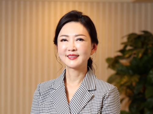
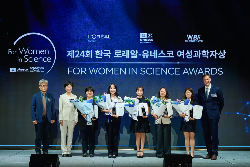 KAIST's Lim Mi-hee wins Korea's L'Oréal-UNESCO Women in Science Award
Lim Mi-hee, a professor at the Korea Advanced Institute of Science and Technology (KAIST) Department of Chemistry, received the Academic Promotion Award at the 24th Korean L'Oréal-UNESCO Women in Science Awards ceremony.
L'Oréal Korea, the Korean National Commission for UNESCO, and the Women’s Bioscience Forum held the 24th Korean L'Oréal-UNESCO Women in Science Awards ceremony on the 16th and noted that Lim Mi-hee was selected for this year’s Academic Promotion Award.
Professor Lim was recognized for her research on the causes of Alzheimer's disease at the molecular level and her efforts in the discovery of intracellular proteins that promote the toxicity of Alzheimer’s-inducing factors. Professor Lim is a full member of the Korean Academy of Science and Technology (KAST) and has received several awards including the Hanseong Science Award, this year's Women in Science and Technology Award, and the RIGAKU-ACCC Award (Asia's top woman scientist).
The fellowship section, awarded to four emerging women scientists, includes Kang Mi-kyung, an assistant professor at Korea University’s Department of Health and Environmental Sciences; Jeon Ji-hye, an assistant professor at Gyeongsang National University’s Department of Life Sciences; Jo Yu-na, a research professor at Pusan National University’s College of Medicine; and Lee Jeong-hyun, an assistant professor at Kongju National University’s Department of Environmental Education.
The recipients of the Academic Promotion Award and fellowships will receive a certificate and a trophy, along with research funding of 30 million won and 7 million won, respectively.
Samuel du Retail, the representative of L'Oréal Korea, said, “The L'Oréal Group continues to support the empowerment of women scientists and the improvement of research environments worldwide under the philosophy that 'the world needs science, and science needs women.' We will actively support more female talents to shine at the center of scientific and technological advancement in the future.”
2025.07.18 View 262
KAIST's Lim Mi-hee wins Korea's L'Oréal-UNESCO Women in Science Award
Lim Mi-hee, a professor at the Korea Advanced Institute of Science and Technology (KAIST) Department of Chemistry, received the Academic Promotion Award at the 24th Korean L'Oréal-UNESCO Women in Science Awards ceremony.
L'Oréal Korea, the Korean National Commission for UNESCO, and the Women’s Bioscience Forum held the 24th Korean L'Oréal-UNESCO Women in Science Awards ceremony on the 16th and noted that Lim Mi-hee was selected for this year’s Academic Promotion Award.
Professor Lim was recognized for her research on the causes of Alzheimer's disease at the molecular level and her efforts in the discovery of intracellular proteins that promote the toxicity of Alzheimer’s-inducing factors. Professor Lim is a full member of the Korean Academy of Science and Technology (KAST) and has received several awards including the Hanseong Science Award, this year's Women in Science and Technology Award, and the RIGAKU-ACCC Award (Asia's top woman scientist).
The fellowship section, awarded to four emerging women scientists, includes Kang Mi-kyung, an assistant professor at Korea University’s Department of Health and Environmental Sciences; Jeon Ji-hye, an assistant professor at Gyeongsang National University’s Department of Life Sciences; Jo Yu-na, a research professor at Pusan National University’s College of Medicine; and Lee Jeong-hyun, an assistant professor at Kongju National University’s Department of Environmental Education.
The recipients of the Academic Promotion Award and fellowships will receive a certificate and a trophy, along with research funding of 30 million won and 7 million won, respectively.
Samuel du Retail, the representative of L'Oréal Korea, said, “The L'Oréal Group continues to support the empowerment of women scientists and the improvement of research environments worldwide under the philosophy that 'the world needs science, and science needs women.' We will actively support more female talents to shine at the center of scientific and technological advancement in the future.”
2025.07.18 View 262 -
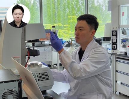 Military Combatants Usher in an Era of Personalized Training with New Materials
< Photo 1. (From left) Professor Steve Park of Materials Science and Engineering, Kyusoon Pak, Ph.D. Candidate (Army Major) >
Traditional military training often relies on standardized methods, which has limited the provision of optimized training tailored to individual combatants' characteristics or specific combat situations. To address this, our research team developed an e-textile platform, securing core technology that can reflect the unique traits of individual combatants and various combat scenarios. This technology has proven robust enough for battlefield use and is economical enough for widespread distribution to a large number of troops.
On June 25th, Professor Steve Park's research team at KAIST's Department of Materials Science and Engineering announced the development of a flexible, wearable electronic textile (E-textile) platform using an innovative technology that 'draws' electronic circuits directly onto fabric.
The wearable e-textile platform developed by the research team combines 3D printing technology with new materials engineering design to directly print flexible and highly durable sensors and electrodes onto textile substrates. This enables the collection of precise movement and human body data from individual combatants, which can then be used to propose customized training models.
Existing e-textile fabrication methods were often complex or limited in their ability to provide personalized customization. To overcome these challenges, the research team adopted an additive manufacturing technology called 'Direct Ink Writing (DIW)' 3D printing.
< Figure 1. Schematic diagram of e-textile manufactured with Direct Ink Writing (DIW) printing technology on various textiles, including combat uniforms >
This technology involves directly dispensing and printing special ink, which functions as sensors and electrodes, onto textile substrates in desired patterns. This allows for flexible implementation of various designs without the complex process of mask fabrication. This is expected to be an effective technology that can be easily supplied to hundreds of thousands of military personnel.
The core of this technology lies in the development of high-performance functional inks based on advanced materials engineering design. The research team combined styrene-butadiene-styrene (SBS) polymer, which provides flexibility, with multi-walled carbon nanotubes (MWCNT) for electrical conductivity. They developed a tensile/bending sensor ink that can stretch up to 102% and maintain stable performance even after 10,000 repetitive tests. This means that accurate data can be consistently obtained even during the strenuous movements of combatants.
< Figure 2. Measurement of human movement and breathing patterns using e-textile >
Furthermore, new material technology was applied to implement 'interconnect electrodes' that electrically connect the upper and lower layers of the fabric. The team developed an electrode ink combining silver (Ag) flakes with rigid polystyrene (PS) polymer, precisely controlling the impregnation level (how much the ink penetrates the fabric) to effectively connect both sides or multiple layers of the fabric. This secures the technology for producing multi-layered wearable electronic systems integrating sensors and electrodes.
< Figure 3. Experimental results of recognizing unknown objects after machine learning six objects using a smart glove >
The research team proved the platform's performance through actual human movement monitoring experiments. They printed the developed e-textile on major joint areas of clothing (shoulders, elbows, knees) and measured movements and posture changes during various exercises such as running, jumping jacks, and push-ups in real-time.
Additionally, they demonstrated the potential for applications such as monitoring breathing patterns using a smart mask and recognizing objects through machine learning and perceiving complex tactile information by printing multiple sensors and electrodes on gloves. These results show that the developed e-textile platform is effective in precisely understanding the movement dynamics of combatants.
This research is an important example demonstrating how cutting-edge new material technology can contribute to the advancement of the defense sector. Major Kyusoon Pak of the Army, who participated in this research, considered required objectives such as military applicability and economic feasibility for practical distribution from the research design stage.
< Figure 4. Experimental results showing that a multi-layered e-textile glove connected with interconnect electrodes can measure tensile/bending signals and pressure signals at a single point >
Major Pak stated, "Our military is currently facing both a crisis and an opportunity due to the decrease in military personnel resources caused by the demographic cliff and the advancement of science and technology. Also, respect for life in the battlefield is emerging as a significant issue. This research aims to secure original technology that can provide customized training according to military branch/duty and type of combat, thereby enhancing the combat power and ensuring the survivability of our soldiers."
He added, "I hope this research will be evaluated as a case that achieved both scientific contribution and military applicability."
This research, where Kyusoon Pak, Ph.D. Candidate (Army Major) from KAIST's Department of Materials Science and Engineering, participated as the first author and Professor Steve Park supervised, was published on May 27, 2025, in `npj Flexible Electronics (top 1.8% in JCR field)', an international academic journal in the electrical, electronic, and materials engineering fields.
* Paper Title: Fabrication of Multifunctional Wearable Interconnect E-textile Platform Using Direct Ink Writing (DIW) 3D Printing
* DOI: https://doi.org/10.1038/s41528-025-00414-7
This research was supported by the Ministry of Trade, Industry and Energy and the National Research Foundation of Korea.
2025.06.25 View 1868
Military Combatants Usher in an Era of Personalized Training with New Materials
< Photo 1. (From left) Professor Steve Park of Materials Science and Engineering, Kyusoon Pak, Ph.D. Candidate (Army Major) >
Traditional military training often relies on standardized methods, which has limited the provision of optimized training tailored to individual combatants' characteristics or specific combat situations. To address this, our research team developed an e-textile platform, securing core technology that can reflect the unique traits of individual combatants and various combat scenarios. This technology has proven robust enough for battlefield use and is economical enough for widespread distribution to a large number of troops.
On June 25th, Professor Steve Park's research team at KAIST's Department of Materials Science and Engineering announced the development of a flexible, wearable electronic textile (E-textile) platform using an innovative technology that 'draws' electronic circuits directly onto fabric.
The wearable e-textile platform developed by the research team combines 3D printing technology with new materials engineering design to directly print flexible and highly durable sensors and electrodes onto textile substrates. This enables the collection of precise movement and human body data from individual combatants, which can then be used to propose customized training models.
Existing e-textile fabrication methods were often complex or limited in their ability to provide personalized customization. To overcome these challenges, the research team adopted an additive manufacturing technology called 'Direct Ink Writing (DIW)' 3D printing.
< Figure 1. Schematic diagram of e-textile manufactured with Direct Ink Writing (DIW) printing technology on various textiles, including combat uniforms >
This technology involves directly dispensing and printing special ink, which functions as sensors and electrodes, onto textile substrates in desired patterns. This allows for flexible implementation of various designs without the complex process of mask fabrication. This is expected to be an effective technology that can be easily supplied to hundreds of thousands of military personnel.
The core of this technology lies in the development of high-performance functional inks based on advanced materials engineering design. The research team combined styrene-butadiene-styrene (SBS) polymer, which provides flexibility, with multi-walled carbon nanotubes (MWCNT) for electrical conductivity. They developed a tensile/bending sensor ink that can stretch up to 102% and maintain stable performance even after 10,000 repetitive tests. This means that accurate data can be consistently obtained even during the strenuous movements of combatants.
< Figure 2. Measurement of human movement and breathing patterns using e-textile >
Furthermore, new material technology was applied to implement 'interconnect electrodes' that electrically connect the upper and lower layers of the fabric. The team developed an electrode ink combining silver (Ag) flakes with rigid polystyrene (PS) polymer, precisely controlling the impregnation level (how much the ink penetrates the fabric) to effectively connect both sides or multiple layers of the fabric. This secures the technology for producing multi-layered wearable electronic systems integrating sensors and electrodes.
< Figure 3. Experimental results of recognizing unknown objects after machine learning six objects using a smart glove >
The research team proved the platform's performance through actual human movement monitoring experiments. They printed the developed e-textile on major joint areas of clothing (shoulders, elbows, knees) and measured movements and posture changes during various exercises such as running, jumping jacks, and push-ups in real-time.
Additionally, they demonstrated the potential for applications such as monitoring breathing patterns using a smart mask and recognizing objects through machine learning and perceiving complex tactile information by printing multiple sensors and electrodes on gloves. These results show that the developed e-textile platform is effective in precisely understanding the movement dynamics of combatants.
This research is an important example demonstrating how cutting-edge new material technology can contribute to the advancement of the defense sector. Major Kyusoon Pak of the Army, who participated in this research, considered required objectives such as military applicability and economic feasibility for practical distribution from the research design stage.
< Figure 4. Experimental results showing that a multi-layered e-textile glove connected with interconnect electrodes can measure tensile/bending signals and pressure signals at a single point >
Major Pak stated, "Our military is currently facing both a crisis and an opportunity due to the decrease in military personnel resources caused by the demographic cliff and the advancement of science and technology. Also, respect for life in the battlefield is emerging as a significant issue. This research aims to secure original technology that can provide customized training according to military branch/duty and type of combat, thereby enhancing the combat power and ensuring the survivability of our soldiers."
He added, "I hope this research will be evaluated as a case that achieved both scientific contribution and military applicability."
This research, where Kyusoon Pak, Ph.D. Candidate (Army Major) from KAIST's Department of Materials Science and Engineering, participated as the first author and Professor Steve Park supervised, was published on May 27, 2025, in `npj Flexible Electronics (top 1.8% in JCR field)', an international academic journal in the electrical, electronic, and materials engineering fields.
* Paper Title: Fabrication of Multifunctional Wearable Interconnect E-textile Platform Using Direct Ink Writing (DIW) 3D Printing
* DOI: https://doi.org/10.1038/s41528-025-00414-7
This research was supported by the Ministry of Trade, Industry and Energy and the National Research Foundation of Korea.
2025.06.25 View 1868 -
 KAIST to Lead the Way in Nurturing Talent and Driving S&T Innovation for a G3 AI Powerhouse
* Focusing on nurturing talent and dedicating to R&D to become a G3 AI powerhouse (Top 3 AI Nations).
* Leading the realization of an "AI-driven Basic Society for All" and developing technologies that leverage AI to overcome the crisis in Korea's manufacturing sector.
* 50 years ago, South Korea emerged as a scientific and technological powerhouse from the ashes, with KAIST at its core, contributing to the development of scientific and technological talent, innovative technology, national industrial growth, and the creation of a startup innovation ecosystem.
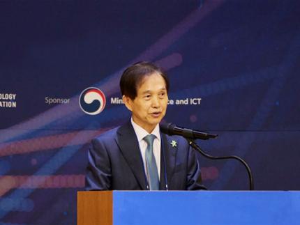
As public interest in AI and science and technology has significantly grown with the inauguration of the new government, KAIST (President Kwang Hyung Lee) announced its plan, on June 24th, to transform into an "AI-centric, Value-Creating Science and Technology University" that leads national innovation based on science and technology and spearheads solutions to global challenges.
At a time when South Korea is undergoing a major transition to a technology-driven society, KAIST, drawing on its half-century of experience as a "Starter Kit" for national development, is preparing to leap beyond being a mere educational and research institution to become a global innovation hub that creates new social value.
In particular, KAIST has presented a vision for realizing an "AI-driven Basic Society" where all citizens can utilize AI without alienation, enabling South Korea to ascend to the top three AI nations (G3). To achieve this, through the "National AI Research Hub" project (headed by Kee Eung Kim), led by KAIST representing South Korea, the institution is dedicated to enhancing industrial competitiveness and effectively solving social problems based on AI technology.
< KAIST President Kwang Hyung Lee >
KAIST's research achievements in the AI field are garnering international attention. In the top three machine learning conferences (ICML, NeurIPS, ICLR), KAIST ranked 5th globally and 1st in Asia over the past five years (2020-2024). During the same period, based on the number of papers published in top conferences in machine learning, natural language processing, and computer vision (ICML, NeurIPS, ICLR, ACL, EMNLP, NAACL, CVPR, ICCV, ECCV), KAIST ranked 5th globally and 4th in Asia. Furthermore, KAIST has consistently demonstrated unparalleled research capabilities, ranking 1st globally in the average number of papers accepted at ISSCC (International Solid-State Circuits Conference), the world's most prestigious academic conference on semiconductor integrated circuits, for 19 years (2006-2024).
KAIST is continuously expanding its research into core AI technologies, including hyper-scale AI models (Korean LLM), neuromorphic semiconductors, and low-power AI processors, as well as various application areas such as autonomous driving, urban air mobility (UAM), precision medicine, and explainable AI (XAI).
In the manufacturing sector, KAIST's AI technologies are also driving on-site innovation. Professor Young Jae Jang's team has enhanced productivity in advanced manufacturing fields like semiconductors and displays through digital twins utilizing manufacturing site data and AI-based prediction technology. Professor Song Min Kim's team developed ultra-low power wireless tag technology capable of tracking locations with sub-centimeter precision, accelerating the implementation of smart factories. Technologies such as industrial process optimization and equipment failure prediction developed by INEEJI Co., Ltd., founded by Professor Jaesik Choi, are being rapidly applied in real industrial settings, yielding results. INEEJI was designated as a national strategic technology in the 'Explainable AI (XAI)' field by the government in March.
< Researchers performing data analysis for AI research >
Practical applications are also emerging in the robotics sector, which is closely linked to AI. Professor Jemin Hwangbo's team from the Department of Mechanical Engineering garnered attention by newly developing RAIBO 2, a quadrupedal robot usable in high-risk environments such as disaster relief and rough terrain exploration. Professor Kyoung Chul Kong's team and Angel Robotics Co., Ltd. developed the WalkOn Suit exoskeleton robot, significantly improving the quality of life for individuals with complete lower body paralysis or walking disabilities.
Additionally, remarkable research is ongoing in future core technology areas such as AI semiconductors, quantum cryptography communication, ultra-small satellites, hydrogen fuel cells, next-generation batteries, and biomimetic sensors. Notably, space exploration technology based on small satellites, asteroid exploration projects, energy harvesting, and high-speed charging technologies are gaining attention.
Particularly in advanced bio and life sciences, KAIST is collaborating with Germany's Merck company on various research initiatives, including synthetic biology and mRNA. KAIST is also contributing to the construction of a 430 billion won Merck Bio-Center in Daejeon, thereby stimulating the local economy and creating jobs.
Based on these cutting-edge research capabilities, KAIST continues to expand its influence not only within the industry but also on the global stage. It has established strategic partnerships with leading universities worldwide, including MIT, Stanford University, and New York University (NYU). Notably, KAIST and NYU have established a joint campus in New York to strengthen human exchange and collaborative research. Active industry-academia collaborations with global companies such as Google, Intel, and TSMC are also ongoing, playing a pivotal role in future technology development and the creation of an innovation ecosystem.
These activities also lead to a strong startup ecosystem that drives South Korean industries. The flow of startups, which began with companies like Qnix Computer, Nexon, and Naver, has expanded to a total of 1,914 companies to date. Their cumulative assets amount to 94 trillion won, with sales reaching 36 trillion won and employing approximately 60,000 people. Over 90% of these are technology-based startups originating from faculty and student labs, demonstrating a model that makes a tangible economic contribution based on science and technology.
< Students at work >
Having consistently generated diverse achievements, KAIST has already produced approximately 80,000 "KAISTians" who have created innovation through challenge and failure, and is currently recruiting new talent to continue driving innovation that transforms South Korea and the world.
President Kwang Hyung Lee emphasized, "KAIST will establish itself as a global leader in science and technology, designing the future of South Korea and humanity and creating tangible value." He added, "We will focus on talent nurturing and research and development to realize the new government's national agenda of becoming a G3 AI powerhouse."
He further stated, "KAIST's vision for the AI field, in which it places particular emphasis, is to strive for a society where everyone can freely utilize AI. We will contribute to significantly boosting productivity by recovering manufacturing competitiveness through AI and actively disseminating physical AI, AI robots, and AI mobility technologies to industrial sites."
2025.06.24 View 2323
KAIST to Lead the Way in Nurturing Talent and Driving S&T Innovation for a G3 AI Powerhouse
* Focusing on nurturing talent and dedicating to R&D to become a G3 AI powerhouse (Top 3 AI Nations).
* Leading the realization of an "AI-driven Basic Society for All" and developing technologies that leverage AI to overcome the crisis in Korea's manufacturing sector.
* 50 years ago, South Korea emerged as a scientific and technological powerhouse from the ashes, with KAIST at its core, contributing to the development of scientific and technological talent, innovative technology, national industrial growth, and the creation of a startup innovation ecosystem.
As public interest in AI and science and technology has significantly grown with the inauguration of the new government, KAIST (President Kwang Hyung Lee) announced its plan, on June 24th, to transform into an "AI-centric, Value-Creating Science and Technology University" that leads national innovation based on science and technology and spearheads solutions to global challenges.
At a time when South Korea is undergoing a major transition to a technology-driven society, KAIST, drawing on its half-century of experience as a "Starter Kit" for national development, is preparing to leap beyond being a mere educational and research institution to become a global innovation hub that creates new social value.
In particular, KAIST has presented a vision for realizing an "AI-driven Basic Society" where all citizens can utilize AI without alienation, enabling South Korea to ascend to the top three AI nations (G3). To achieve this, through the "National AI Research Hub" project (headed by Kee Eung Kim), led by KAIST representing South Korea, the institution is dedicated to enhancing industrial competitiveness and effectively solving social problems based on AI technology.
< KAIST President Kwang Hyung Lee >
KAIST's research achievements in the AI field are garnering international attention. In the top three machine learning conferences (ICML, NeurIPS, ICLR), KAIST ranked 5th globally and 1st in Asia over the past five years (2020-2024). During the same period, based on the number of papers published in top conferences in machine learning, natural language processing, and computer vision (ICML, NeurIPS, ICLR, ACL, EMNLP, NAACL, CVPR, ICCV, ECCV), KAIST ranked 5th globally and 4th in Asia. Furthermore, KAIST has consistently demonstrated unparalleled research capabilities, ranking 1st globally in the average number of papers accepted at ISSCC (International Solid-State Circuits Conference), the world's most prestigious academic conference on semiconductor integrated circuits, for 19 years (2006-2024).
KAIST is continuously expanding its research into core AI technologies, including hyper-scale AI models (Korean LLM), neuromorphic semiconductors, and low-power AI processors, as well as various application areas such as autonomous driving, urban air mobility (UAM), precision medicine, and explainable AI (XAI).
In the manufacturing sector, KAIST's AI technologies are also driving on-site innovation. Professor Young Jae Jang's team has enhanced productivity in advanced manufacturing fields like semiconductors and displays through digital twins utilizing manufacturing site data and AI-based prediction technology. Professor Song Min Kim's team developed ultra-low power wireless tag technology capable of tracking locations with sub-centimeter precision, accelerating the implementation of smart factories. Technologies such as industrial process optimization and equipment failure prediction developed by INEEJI Co., Ltd., founded by Professor Jaesik Choi, are being rapidly applied in real industrial settings, yielding results. INEEJI was designated as a national strategic technology in the 'Explainable AI (XAI)' field by the government in March.
< Researchers performing data analysis for AI research >
Practical applications are also emerging in the robotics sector, which is closely linked to AI. Professor Jemin Hwangbo's team from the Department of Mechanical Engineering garnered attention by newly developing RAIBO 2, a quadrupedal robot usable in high-risk environments such as disaster relief and rough terrain exploration. Professor Kyoung Chul Kong's team and Angel Robotics Co., Ltd. developed the WalkOn Suit exoskeleton robot, significantly improving the quality of life for individuals with complete lower body paralysis or walking disabilities.
Additionally, remarkable research is ongoing in future core technology areas such as AI semiconductors, quantum cryptography communication, ultra-small satellites, hydrogen fuel cells, next-generation batteries, and biomimetic sensors. Notably, space exploration technology based on small satellites, asteroid exploration projects, energy harvesting, and high-speed charging technologies are gaining attention.
Particularly in advanced bio and life sciences, KAIST is collaborating with Germany's Merck company on various research initiatives, including synthetic biology and mRNA. KAIST is also contributing to the construction of a 430 billion won Merck Bio-Center in Daejeon, thereby stimulating the local economy and creating jobs.
Based on these cutting-edge research capabilities, KAIST continues to expand its influence not only within the industry but also on the global stage. It has established strategic partnerships with leading universities worldwide, including MIT, Stanford University, and New York University (NYU). Notably, KAIST and NYU have established a joint campus in New York to strengthen human exchange and collaborative research. Active industry-academia collaborations with global companies such as Google, Intel, and TSMC are also ongoing, playing a pivotal role in future technology development and the creation of an innovation ecosystem.
These activities also lead to a strong startup ecosystem that drives South Korean industries. The flow of startups, which began with companies like Qnix Computer, Nexon, and Naver, has expanded to a total of 1,914 companies to date. Their cumulative assets amount to 94 trillion won, with sales reaching 36 trillion won and employing approximately 60,000 people. Over 90% of these are technology-based startups originating from faculty and student labs, demonstrating a model that makes a tangible economic contribution based on science and technology.
< Students at work >
Having consistently generated diverse achievements, KAIST has already produced approximately 80,000 "KAISTians" who have created innovation through challenge and failure, and is currently recruiting new talent to continue driving innovation that transforms South Korea and the world.
President Kwang Hyung Lee emphasized, "KAIST will establish itself as a global leader in science and technology, designing the future of South Korea and humanity and creating tangible value." He added, "We will focus on talent nurturing and research and development to realize the new government's national agenda of becoming a G3 AI powerhouse."
He further stated, "KAIST's vision for the AI field, in which it places particular emphasis, is to strive for a society where everyone can freely utilize AI. We will contribute to significantly boosting productivity by recovering manufacturing competitiveness through AI and actively disseminating physical AI, AI robots, and AI mobility technologies to industrial sites."
2025.06.24 View 2323 -
 KAIST perfectly reproduces Joseon-era Irworobongdo without pigments
Typically, chemical pigments that absorb specific wavelengths of light within the visible spectrum are required to produce colors. However, KAIST researchers have successfully reproduced the Joseon-era Irworobongdo [일월오봉도] painting using ultra-precise color graphics without any chemical pigments, allowing for the permanent and eco-friendly preservation of color graphics without fading or discoloration.
< (From left) Chaerim Son, a graduate of the Department of Biochemical Engineering (lead author), Seong Kyeong Nam, a graduate of the PhD program, Jiwoo Lee, a PhD student, and Professor Shin-Hyun Kim >
KAIST (represented by President Kwang Hyung Lee) announced on the 26th of February that a research team led by Professor Shinhyun Kim from the Department of Biological and Chemical Engineering had developed a technology that enables high-resolution color graphics without using any chemical pigments by employing hemisphere-shaped microstructures.
Morpho butterflies that are brilliant blue in color or Panther chameleons that change skin color exhibit coloration without chemical pigments, as ordered nanostructures within a material reflect visible light through optical interference. Since structural colors arise from physical structures rather than chemical substances, a single material can produce a wide range of colors.
However, the artificial implementation of structural coloration is highly challenging due to the complexity of creating ordered nanostructures. Additionally, it is difficult to produce a variety of colors and to pattern them precisely into complex designs.
< Figure 1. Principle of structural color expression using micro-hemispheres (left) and method of forming micro-hemisphere patterns based on photolithography (right) >
Professor Kim’s team overcame these challenges by using smooth-surfaced hemispherical microstructures instead of ordered nanostructures, enabling the high-precision patterning of diverse structural colors.
When light enters the inverted hemispherical microstructures, the portion of light entering from the sides undergoes total internal reflection along the curved surface, creating retroreflection. When the hemisphere diameter is approximately 10 micrometers (about one-tenth the thickness of a human hair), light traveling along different reflection paths interferes within the visible spectrum, producing structural coloration.
< Figure 2. “Irworobongdo”, the Painting of the Sun, Moon, and the Five Peaks, reproduced in fingernail size without pigment using approximately 200,000 micro-hemispheres >
The structural color can be tuned by adjusting the size of the hemispheres. By arranging hemispheres of varying sizes, much like mixing paints on a palette, an infinite range of colors can be generated.
To precisely pattern microscale hemispheres of different sizes, the research team employed photolithography* using positive photoresists** commonly used in semiconductor processing. They first patterned photoresists into micropillar structures, then induced reflow*** by heating the material, forming hemispherical microstructures.
*Photolithography: A technique used in semiconductor fabrication to pattern microscale structures.
**Positive photoresist: A photosensitive polymer that dissolves more easily in a developer solution after exposure to ultraviolet light.
***Reflow: A process in which a polymer material softens and reshapes into a curved structure when heated.
This method enables the formation of hemisphere-shaped microstructures with the desired sizes and colors in a single-step fabrication process. It also allows for the reproduction of arbitrary color graphics using a single material without any pigments.
The ultra-precise color graphics created with this technique can exhibit color variations depending on the angle of incident light or the viewing perspective. The pattern appears colored from one direction while remaining transparent from the opposite side, exhibiting a Janus effect. These structural color graphics achieve resolution comparable to cutting-edge LED displays, allowing complex color images to be captured within a fingernail-sized area and projected onto large screens.
< Figure 3. “Irworobongdo” that displays different shades depending on the angle of light and viewing direction >
Professor Shinhyun Kim, who led the research, stated, “Our newly developed pigment-free color graphics technology can serve as an innovative method for artistic expression, merging art with advanced materials. Additionally, it holds broad application potential in optical devices and sensors, anti-counterfeiting materials, aesthetic photocard printing, and many other fields.”
This research, with KAIST researcher Chaerim Son as the first author, was published in the prestigious materials science journal Advanced Materials on February 5.
(Paper title: “Retroreflective Multichrome Microdome Arrays Created by Single-Step Reflow”, DOI: 10.1002/adma.202413143 )
< Figure 4. Famous paintings reproduced without pigment: “Impression, Sunrise” (left), “Girl with a Pearl Earring” (right) >
The study was supported by the National Research Foundation of Korea through the Pioneer Converging Technology R&D Program and the Mid-Career Researcher Program.
2025.02.26 View 5678
KAIST perfectly reproduces Joseon-era Irworobongdo without pigments
Typically, chemical pigments that absorb specific wavelengths of light within the visible spectrum are required to produce colors. However, KAIST researchers have successfully reproduced the Joseon-era Irworobongdo [일월오봉도] painting using ultra-precise color graphics without any chemical pigments, allowing for the permanent and eco-friendly preservation of color graphics without fading or discoloration.
< (From left) Chaerim Son, a graduate of the Department of Biochemical Engineering (lead author), Seong Kyeong Nam, a graduate of the PhD program, Jiwoo Lee, a PhD student, and Professor Shin-Hyun Kim >
KAIST (represented by President Kwang Hyung Lee) announced on the 26th of February that a research team led by Professor Shinhyun Kim from the Department of Biological and Chemical Engineering had developed a technology that enables high-resolution color graphics without using any chemical pigments by employing hemisphere-shaped microstructures.
Morpho butterflies that are brilliant blue in color or Panther chameleons that change skin color exhibit coloration without chemical pigments, as ordered nanostructures within a material reflect visible light through optical interference. Since structural colors arise from physical structures rather than chemical substances, a single material can produce a wide range of colors.
However, the artificial implementation of structural coloration is highly challenging due to the complexity of creating ordered nanostructures. Additionally, it is difficult to produce a variety of colors and to pattern them precisely into complex designs.
< Figure 1. Principle of structural color expression using micro-hemispheres (left) and method of forming micro-hemisphere patterns based on photolithography (right) >
Professor Kim’s team overcame these challenges by using smooth-surfaced hemispherical microstructures instead of ordered nanostructures, enabling the high-precision patterning of diverse structural colors.
When light enters the inverted hemispherical microstructures, the portion of light entering from the sides undergoes total internal reflection along the curved surface, creating retroreflection. When the hemisphere diameter is approximately 10 micrometers (about one-tenth the thickness of a human hair), light traveling along different reflection paths interferes within the visible spectrum, producing structural coloration.
< Figure 2. “Irworobongdo”, the Painting of the Sun, Moon, and the Five Peaks, reproduced in fingernail size without pigment using approximately 200,000 micro-hemispheres >
The structural color can be tuned by adjusting the size of the hemispheres. By arranging hemispheres of varying sizes, much like mixing paints on a palette, an infinite range of colors can be generated.
To precisely pattern microscale hemispheres of different sizes, the research team employed photolithography* using positive photoresists** commonly used in semiconductor processing. They first patterned photoresists into micropillar structures, then induced reflow*** by heating the material, forming hemispherical microstructures.
*Photolithography: A technique used in semiconductor fabrication to pattern microscale structures.
**Positive photoresist: A photosensitive polymer that dissolves more easily in a developer solution after exposure to ultraviolet light.
***Reflow: A process in which a polymer material softens and reshapes into a curved structure when heated.
This method enables the formation of hemisphere-shaped microstructures with the desired sizes and colors in a single-step fabrication process. It also allows for the reproduction of arbitrary color graphics using a single material without any pigments.
The ultra-precise color graphics created with this technique can exhibit color variations depending on the angle of incident light or the viewing perspective. The pattern appears colored from one direction while remaining transparent from the opposite side, exhibiting a Janus effect. These structural color graphics achieve resolution comparable to cutting-edge LED displays, allowing complex color images to be captured within a fingernail-sized area and projected onto large screens.
< Figure 3. “Irworobongdo” that displays different shades depending on the angle of light and viewing direction >
Professor Shinhyun Kim, who led the research, stated, “Our newly developed pigment-free color graphics technology can serve as an innovative method for artistic expression, merging art with advanced materials. Additionally, it holds broad application potential in optical devices and sensors, anti-counterfeiting materials, aesthetic photocard printing, and many other fields.”
This research, with KAIST researcher Chaerim Son as the first author, was published in the prestigious materials science journal Advanced Materials on February 5.
(Paper title: “Retroreflective Multichrome Microdome Arrays Created by Single-Step Reflow”, DOI: 10.1002/adma.202413143 )
< Figure 4. Famous paintings reproduced without pigment: “Impression, Sunrise” (left), “Girl with a Pearl Earring” (right) >
The study was supported by the National Research Foundation of Korea through the Pioneer Converging Technology R&D Program and the Mid-Career Researcher Program.
2025.02.26 View 5678 -
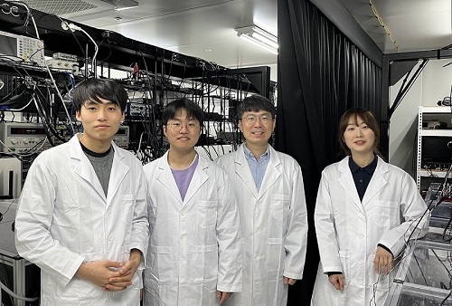 KAIST achieves quantum entanglement essential for quantum error correction
Quantum computing is a technology capable of solving complex problems that classical computers struggle with. To perform accurate computations, quantum computers must correct errors that arise during operations. However, generating the quantum entanglement necessary for quantum error correction has long been considered a major challenge.
< Photo 1. (From left) Students Young-Do Yoon and Chan Roh of the Master's and Doctoral Integrated Program of the Department of Physics poses with Professor Young-Sik Ra and Student Geunhee Gwak of the same program >
KAIST (represented by President Kwang Hyung Lee) announced on the 25th of February that a research team led by Professor Young-Sik Ra from the Department of Physics has successfully implemented a three-dimensional cluster quantum entangled state, a key component for quantum error correction, through experimental demonstration.
Measurement-based quantum computing is an emerging paradigm that implements quantum computations by measuring specially entangled cluster states. The core of this approach lies in the generation of these cluster quantum entangled states, with two-dimensional cluster states commonly used for universal quantum computing.
However, to advance towards fault-tolerant quantum computing, which can correct quantum errors occurring during computations, a more complex three-dimensional cluster state is required. While previous studies have reported the generation of two-dimensional cluster states, experimental implementation of the three-dimensional cluster states necessary for fault-tolerant quantum computing had remained elusive due to the extreme complexity of their entanglement structure.
< Figure 1. (a) Experimental schematic. A pulse laser with a wavelength of 800 nm is converted into a pulse laser with a wavelength of 400 nm through second harmonic generation, and this is incident on a nonlinear crystal (PPKTP) to generate multiple quantum entanglement sources. (b) Generation of a 3D cluster state through optical mode basis change >
The research team overcame this challenge by developing a technique to control femtosecond time-frequency modes, successfully generating a three-dimensional cluster quantum entangled state for the first time.
The team directed a femtosecond laser into a nonlinear crystal, simultaneously generating quantum light sources across multiple frequency modes. (A femtosecond laser is a device that emits ultrashort, high-intensity light pulses.) Using this approach, they successfully created a three-dimensional cluster quantum entangled state.
Professor Young-Sik Ra noted, “This study marks the first successful demonstration of a three-dimensional cluster quantum entangled state, which was previously difficult to achieve with existing technology. This breakthrough is expected to serve as a crucial stepping stone for future research in measurement-based and fault-tolerant quantum computing.”
< Figure 2. Results of 3D cluster state generation. (a) Nullifier measurement of the cluster state. (b) 3D cluster state reconstructed using quantum state tomography. (c) Confirmation of quantum entanglement characteristics of the 3D cluster state >
The study was published online in Nature Photonics on February 24, 2025. The first author is Chan Roh, a Ph.D. candidate in KAIST’s integrated master’s and doctoral program, with Geunhee Gwak and Youngdo Yoon contributing as co-authors. (Paper title: “Generation of Three-Dimensional Cluster Entangled State”, DOI: 10.1038/s41566-025-01631-2)
This research was supported by the National Research Foundation of Korea (Quantum Computing Technology Development Program, Mid-Career Researcher Support Program, and Quantum Simulator for Materials Innovation Program), the Institute for Information & Communications Technology Planning & Evaluation (Quantum Internet Core Technology Program, University ICT Research Center Support Program), and the U.S. Air Force Research Laboratory.
2025.02.25 View 4383
KAIST achieves quantum entanglement essential for quantum error correction
Quantum computing is a technology capable of solving complex problems that classical computers struggle with. To perform accurate computations, quantum computers must correct errors that arise during operations. However, generating the quantum entanglement necessary for quantum error correction has long been considered a major challenge.
< Photo 1. (From left) Students Young-Do Yoon and Chan Roh of the Master's and Doctoral Integrated Program of the Department of Physics poses with Professor Young-Sik Ra and Student Geunhee Gwak of the same program >
KAIST (represented by President Kwang Hyung Lee) announced on the 25th of February that a research team led by Professor Young-Sik Ra from the Department of Physics has successfully implemented a three-dimensional cluster quantum entangled state, a key component for quantum error correction, through experimental demonstration.
Measurement-based quantum computing is an emerging paradigm that implements quantum computations by measuring specially entangled cluster states. The core of this approach lies in the generation of these cluster quantum entangled states, with two-dimensional cluster states commonly used for universal quantum computing.
However, to advance towards fault-tolerant quantum computing, which can correct quantum errors occurring during computations, a more complex three-dimensional cluster state is required. While previous studies have reported the generation of two-dimensional cluster states, experimental implementation of the three-dimensional cluster states necessary for fault-tolerant quantum computing had remained elusive due to the extreme complexity of their entanglement structure.
< Figure 1. (a) Experimental schematic. A pulse laser with a wavelength of 800 nm is converted into a pulse laser with a wavelength of 400 nm through second harmonic generation, and this is incident on a nonlinear crystal (PPKTP) to generate multiple quantum entanglement sources. (b) Generation of a 3D cluster state through optical mode basis change >
The research team overcame this challenge by developing a technique to control femtosecond time-frequency modes, successfully generating a three-dimensional cluster quantum entangled state for the first time.
The team directed a femtosecond laser into a nonlinear crystal, simultaneously generating quantum light sources across multiple frequency modes. (A femtosecond laser is a device that emits ultrashort, high-intensity light pulses.) Using this approach, they successfully created a three-dimensional cluster quantum entangled state.
Professor Young-Sik Ra noted, “This study marks the first successful demonstration of a three-dimensional cluster quantum entangled state, which was previously difficult to achieve with existing technology. This breakthrough is expected to serve as a crucial stepping stone for future research in measurement-based and fault-tolerant quantum computing.”
< Figure 2. Results of 3D cluster state generation. (a) Nullifier measurement of the cluster state. (b) 3D cluster state reconstructed using quantum state tomography. (c) Confirmation of quantum entanglement characteristics of the 3D cluster state >
The study was published online in Nature Photonics on February 24, 2025. The first author is Chan Roh, a Ph.D. candidate in KAIST’s integrated master’s and doctoral program, with Geunhee Gwak and Youngdo Yoon contributing as co-authors. (Paper title: “Generation of Three-Dimensional Cluster Entangled State”, DOI: 10.1038/s41566-025-01631-2)
This research was supported by the National Research Foundation of Korea (Quantum Computing Technology Development Program, Mid-Career Researcher Support Program, and Quantum Simulator for Materials Innovation Program), the Institute for Information & Communications Technology Planning & Evaluation (Quantum Internet Core Technology Program, University ICT Research Center Support Program), and the U.S. Air Force Research Laboratory.
2025.02.25 View 4383 -
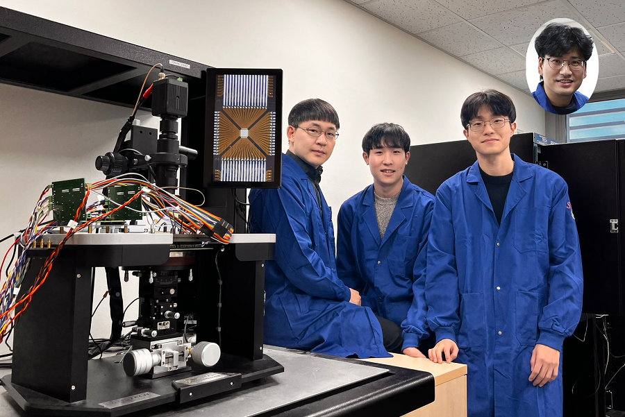 KAIST Develops Neuromorphic Semiconductor Chip that Learns and Corrects Itself
< Photo. The research team of the School of Electrical Engineering posed by the newly deveoped processor. (From center to the right) Professor Young-Gyu Yoon, Integrated Master's and Doctoral Program Students Seungjae Han and Hakcheon Jeong and Professor Shinhyun Choi >
- Professor Shinhyun Choi and Professor Young-Gyu Yoon’s Joint Research Team from the School of Electrical Engineering developed a computing chip that can learn, correct errors, and process AI tasks
- Equipping a computing chip with high-reliability memristor devices with self-error correction functions for real-time learning and image processing
Existing computer systems have separate data processing and storage devices, making them inefficient for processing complex data like AI. A KAIST research team has developed a memristor-based integrated system similar to the way our brain processes information. It is now ready for application in various devices including smart security cameras, allowing them to recognize suspicious activity immediately without having to rely on remote cloud servers, and medical devices with which it can help analyze health data in real time.
KAIST (President Kwang Hyung Lee) announced on the 17th of January that the joint research team of Professor Shinhyun Choi and Professor Young-Gyu Yoon of the School of Electrical Engineering has developed a next-generation neuromorphic semiconductor-based ultra-small computing chip that can learn and correct errors on its own.
< Figure 1. Scanning electron microscope (SEM) image of a computing chip equipped with a highly reliable selector-less 32×32 memristor crossbar array (left). Hardware system developed for real-time artificial intelligence implementation (right). >
What is special about this computing chip is that it can learn and correct errors that occur due to non-ideal characteristics that were difficult to solve in existing neuromorphic devices. For example, when processing a video stream, the chip learns to automatically separate a moving object from the background, and it becomes better at this task over time.
This self-learning ability has been proven by achieving accuracy comparable to ideal computer simulations in real-time image processing. The research team's main achievement is that it has completed a system that is both reliable and practical, beyond the development of brain-like components.
The research team has developed the world's first memristor-based integrated system that can adapt to immediate environmental changes, and has presented an innovative solution that overcomes the limitations of existing technology.
< Figure 2. Background and foreground separation results of an image containing non-ideal characteristics of memristor devices (left). Real-time image separation results through on-device learning using the memristor computing chip developed by our research team (right). >
At the heart of this innovation is a next-generation semiconductor device called a memristor*. The variable resistance characteristics of this device can replace the role of synapses in neural networks, and by utilizing it, data storage and computation can be performed simultaneously, just like our brain cells.
*Memristor: A compound word of memory and resistor, next-generation electrical device whose resistance value is determined by the amount and direction of charge that has flowed between the two terminals in the past.
The research team designed a highly reliable memristor that can precisely control resistance changes and developed an efficient system that excludes complex compensation processes through self-learning. This study is significant in that it experimentally verified the commercialization possibility of a next-generation neuromorphic semiconductor-based integrated system that supports real-time learning and inference.
This technology will revolutionize the way artificial intelligence is used in everyday devices, allowing AI tasks to be processed locally without relying on remote cloud servers, making them faster, more privacy-protected, and more energy-efficient.
“This system is like a smart workspace where everything is within arm’s reach instead of having to go back and forth between desks and file cabinets,” explained KAIST researchers Hakcheon Jeong and Seungjae Han, who led the development of this technology. “This is similar to the way our brain processes information, where everything is processed efficiently at once at one spot.”
The research was conducted with Hakcheon Jeong and Seungjae Han, the students of Integrated Master's and Doctoral Program at KAIST School of Electrical Engineering being the co-first authors, the results of which was published online in the international academic journal, Nature Electronics, on January 8, 2025.
*Paper title: Self-supervised video processing with self-calibration on an analogue computing platform based on a selector-less memristor array ( https://doi.org/10.1038/s41928-024-01318-6 )
This research was supported by the Next-Generation Intelligent Semiconductor Technology Development Project, Excellent New Researcher Project and PIM AI Semiconductor Core Technology Development Project of the National Research Foundation of Korea, and the Electronics and Telecommunications Research Institute Research and Development Support Project of the Institute of Information & communications Technology Planning & Evaluation.
2025.01.17 View 9530
KAIST Develops Neuromorphic Semiconductor Chip that Learns and Corrects Itself
< Photo. The research team of the School of Electrical Engineering posed by the newly deveoped processor. (From center to the right) Professor Young-Gyu Yoon, Integrated Master's and Doctoral Program Students Seungjae Han and Hakcheon Jeong and Professor Shinhyun Choi >
- Professor Shinhyun Choi and Professor Young-Gyu Yoon’s Joint Research Team from the School of Electrical Engineering developed a computing chip that can learn, correct errors, and process AI tasks
- Equipping a computing chip with high-reliability memristor devices with self-error correction functions for real-time learning and image processing
Existing computer systems have separate data processing and storage devices, making them inefficient for processing complex data like AI. A KAIST research team has developed a memristor-based integrated system similar to the way our brain processes information. It is now ready for application in various devices including smart security cameras, allowing them to recognize suspicious activity immediately without having to rely on remote cloud servers, and medical devices with which it can help analyze health data in real time.
KAIST (President Kwang Hyung Lee) announced on the 17th of January that the joint research team of Professor Shinhyun Choi and Professor Young-Gyu Yoon of the School of Electrical Engineering has developed a next-generation neuromorphic semiconductor-based ultra-small computing chip that can learn and correct errors on its own.
< Figure 1. Scanning electron microscope (SEM) image of a computing chip equipped with a highly reliable selector-less 32×32 memristor crossbar array (left). Hardware system developed for real-time artificial intelligence implementation (right). >
What is special about this computing chip is that it can learn and correct errors that occur due to non-ideal characteristics that were difficult to solve in existing neuromorphic devices. For example, when processing a video stream, the chip learns to automatically separate a moving object from the background, and it becomes better at this task over time.
This self-learning ability has been proven by achieving accuracy comparable to ideal computer simulations in real-time image processing. The research team's main achievement is that it has completed a system that is both reliable and practical, beyond the development of brain-like components.
The research team has developed the world's first memristor-based integrated system that can adapt to immediate environmental changes, and has presented an innovative solution that overcomes the limitations of existing technology.
< Figure 2. Background and foreground separation results of an image containing non-ideal characteristics of memristor devices (left). Real-time image separation results through on-device learning using the memristor computing chip developed by our research team (right). >
At the heart of this innovation is a next-generation semiconductor device called a memristor*. The variable resistance characteristics of this device can replace the role of synapses in neural networks, and by utilizing it, data storage and computation can be performed simultaneously, just like our brain cells.
*Memristor: A compound word of memory and resistor, next-generation electrical device whose resistance value is determined by the amount and direction of charge that has flowed between the two terminals in the past.
The research team designed a highly reliable memristor that can precisely control resistance changes and developed an efficient system that excludes complex compensation processes through self-learning. This study is significant in that it experimentally verified the commercialization possibility of a next-generation neuromorphic semiconductor-based integrated system that supports real-time learning and inference.
This technology will revolutionize the way artificial intelligence is used in everyday devices, allowing AI tasks to be processed locally without relying on remote cloud servers, making them faster, more privacy-protected, and more energy-efficient.
“This system is like a smart workspace where everything is within arm’s reach instead of having to go back and forth between desks and file cabinets,” explained KAIST researchers Hakcheon Jeong and Seungjae Han, who led the development of this technology. “This is similar to the way our brain processes information, where everything is processed efficiently at once at one spot.”
The research was conducted with Hakcheon Jeong and Seungjae Han, the students of Integrated Master's and Doctoral Program at KAIST School of Electrical Engineering being the co-first authors, the results of which was published online in the international academic journal, Nature Electronics, on January 8, 2025.
*Paper title: Self-supervised video processing with self-calibration on an analogue computing platform based on a selector-less memristor array ( https://doi.org/10.1038/s41928-024-01318-6 )
This research was supported by the Next-Generation Intelligent Semiconductor Technology Development Project, Excellent New Researcher Project and PIM AI Semiconductor Core Technology Development Project of the National Research Foundation of Korea, and the Electronics and Telecommunications Research Institute Research and Development Support Project of the Institute of Information & communications Technology Planning & Evaluation.
2025.01.17 View 9530 -
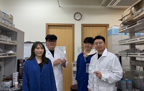
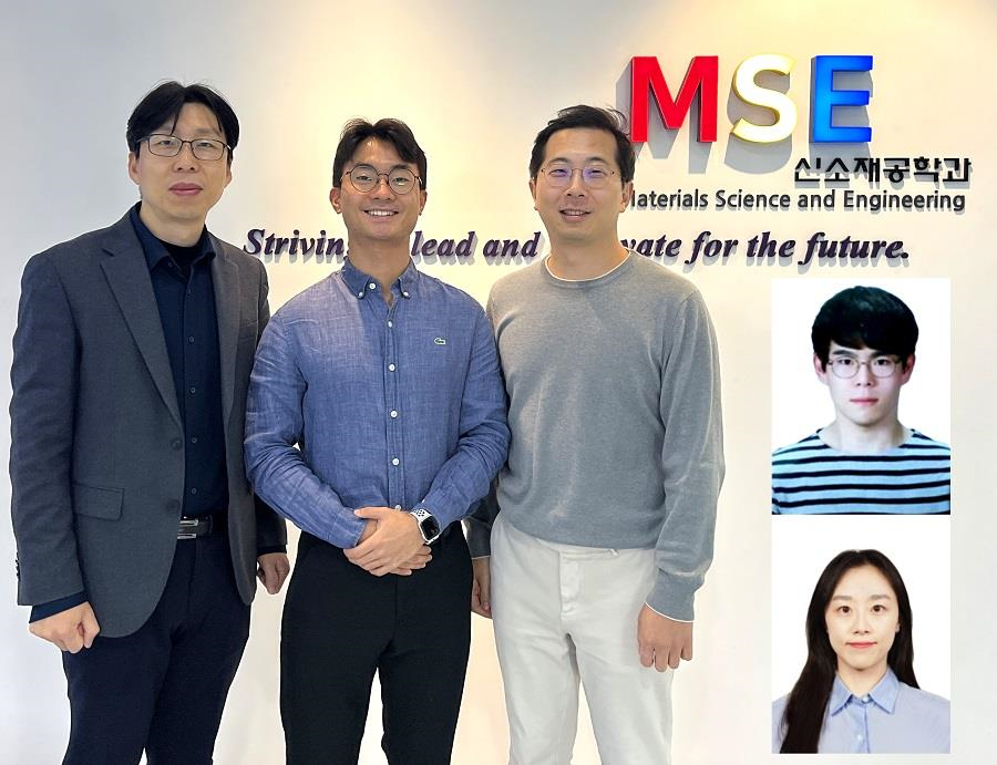 KAIST Develops CamBio - a New Biotemplating Method
- Professor Jae-Byum Chang and Professor Yeon Sik Jung’s joint research team of the Department of Materials Science and Engineering developed a highly tunable bio-templating method “CamBio” that makes use of intracellular protein structures
- Substrate performance improvement of up to 230% demonstrated via surface-enhanced Raman spectroscopy (SERS)
- Expected to have price competitiveness over bio-templating method as it expands the range of biological samples
- Expected to expand the range of application of nanostructure synthesis technology by utilizing various biological structures
< Photo 1. (From left) Professor Yeon Sik Jung, Ph.D. candidate Dae-Hyeon Song, Professor Jae-Byum Chang, and (from top right) Dr. Chang Woo Song and Dr. Seunghee H. Cho of the Department of Materials Science and Engineering >
Biological structures have complex characteristics that are difficult to replicate artificially, but biotemplating methods* that directly utilize these biological structures have been used in various fields of application. The KAIST research team succeeded in utilizing previously unusable biological structures and expanding the areas in which biotemplate methods can be applied.
*Biotemplating: A method of using biotemplates as a mold to create functional structural materials, utilizing the functions of these biological structures, from viruses to the tissues and organs that make up our bodies
KAIST (President Kwang Hyung Lee) announced on the 10th that a joint research team of Professors Jae-Byum Chang and Professor Yeon Sik Jung of the Department of Materials Science and Engineering developed a biotemplating method that utilizes specific intracellular proteins in biological samples and has high tunability.
Existing biotemplate methods mainly utilize only the external surface of biological samples or have limitations in utilizing the structure-function correlation of various biological structures due to limited dimensions and sample sizes, making it difficult to create functional nanostructures.
To solve this problem, the research team studied a way to utilize various biological structures within the cells while retaining high tunability.
< Figure 1. CamBio utilizing microtubules, a intracellular protein structure. The silver nanoparticle chains synthesized along the microtubules that span the entire cell interior can be observed through an electron microscope, and it is shown that this can be used as a successful SERS substrate. >
As a result of the research, the team developed the “Conversion to advanced materials via labeled Biostructure”, shortened as “CamBio”, which enables the selective synthesis of nanostructures with various characteristics and sizes from specific protein structures composed of diverse proteins within biological specimens.
The CamBio method secures high tunability of functional nanostructures that can be manufactured from biological samples by merging various manufacturing and biological technologies.
Through the technology of repeatedly attaching antibodies, arranging cells in a certain shape, and thinly slicing tissue, the functional nanostructures made with CamBio showed improved performance on the surface-enhanced Raman spectroscopy (SERS)* substrate used for material detection.
*Surface-enhanced Raman spectroscopy (SERS): A technology that can detect very small amounts of substances using light, based on the principle that specific substances react to light and amplifies signals on surfaces of metals such as gold or silver.
The research team found that the nanoparticle chains made using the intracellular protein structures through the process of repeated labeling with antibodies allowed easier control, and improved SERS performance by up to 230%.
In addition, the research team expanded from utilizing the structures inside cells to obtaining samples of muscle tissues inside meat using a cryostat and successfully producing a substrate with periodic bands made of metal particles by performing the CamBio process. This method of producing a substrate not only allows large-scale production using biological samples, but also shows that it is a cost-effective method.
< Figure 2. A method for securing tunability using CamBio at the cell level. Examples of controlling characteristics by integrating iterative labeling and cell pattering techniques with CamBio are shown. >
The CamBio developed by the research team is expected to be used as a way to solve problems faced by various research fields as it is to expand the range of bio-samples that can be produced for various usage.
The first author, Dae-Hyeon Song, a Ph.D. candidate of KAIST Department of Materials Science and Engineering said, “Through CamBio, we have comprehensively accumulated biotemplating methods that can utilize more diverse protein structures,” and “If combined with the state-of-the-art biological technologies such as gene editing and 3D bioprinting and new material synthesis technologies, biostructures can be utilized in various fields of application.”
< Figure 3. A method for securing tunability using CamBio at the tissue level. In order to utilize proteins inside muscle tissue, the frozen tissue sectioning technology is combined, and through this, a substrate with a periodic nanoparticle band pattern is successfully produced, and it is shown that large-area acquisition of samples and price competitiveness can be achieved. >
This study, in which the Ph.D. candidate Dae-Hyeon Song along with Dr. Chang Woo Song, and Dr. Seunghee H. Cho of the same department participated as the first authors, was published online in the international academic journal, Advanced Science, on November 13th, 2024.
(Paper title: Highly Tunable, Nanomaterial-Functionalized Structural Templating of Intracellular Protein Structures Within Biological Species) https://doi.org/10.1002/advs.202406492
This study was conducted with a combination of support from various programs including the National Convergence Research of Scientific Challenges (National Research Foundation of Korea (NRF) 2024), Engineering Reseach Center (ERC) (Wearable Platform Materials Technology Center, NRF 2023), ERC (Global Bio-integrated Materials Center, NRF 2024), and the National Advanced Program for Biological Research Resources (Bioimaging Data Curation Center, NRF 2024) funded by Ministry of Science and ICT.
2025.01.10 View 6462
KAIST Develops CamBio - a New Biotemplating Method
- Professor Jae-Byum Chang and Professor Yeon Sik Jung’s joint research team of the Department of Materials Science and Engineering developed a highly tunable bio-templating method “CamBio” that makes use of intracellular protein structures
- Substrate performance improvement of up to 230% demonstrated via surface-enhanced Raman spectroscopy (SERS)
- Expected to have price competitiveness over bio-templating method as it expands the range of biological samples
- Expected to expand the range of application of nanostructure synthesis technology by utilizing various biological structures
< Photo 1. (From left) Professor Yeon Sik Jung, Ph.D. candidate Dae-Hyeon Song, Professor Jae-Byum Chang, and (from top right) Dr. Chang Woo Song and Dr. Seunghee H. Cho of the Department of Materials Science and Engineering >
Biological structures have complex characteristics that are difficult to replicate artificially, but biotemplating methods* that directly utilize these biological structures have been used in various fields of application. The KAIST research team succeeded in utilizing previously unusable biological structures and expanding the areas in which biotemplate methods can be applied.
*Biotemplating: A method of using biotemplates as a mold to create functional structural materials, utilizing the functions of these biological structures, from viruses to the tissues and organs that make up our bodies
KAIST (President Kwang Hyung Lee) announced on the 10th that a joint research team of Professors Jae-Byum Chang and Professor Yeon Sik Jung of the Department of Materials Science and Engineering developed a biotemplating method that utilizes specific intracellular proteins in biological samples and has high tunability.
Existing biotemplate methods mainly utilize only the external surface of biological samples or have limitations in utilizing the structure-function correlation of various biological structures due to limited dimensions and sample sizes, making it difficult to create functional nanostructures.
To solve this problem, the research team studied a way to utilize various biological structures within the cells while retaining high tunability.
< Figure 1. CamBio utilizing microtubules, a intracellular protein structure. The silver nanoparticle chains synthesized along the microtubules that span the entire cell interior can be observed through an electron microscope, and it is shown that this can be used as a successful SERS substrate. >
As a result of the research, the team developed the “Conversion to advanced materials via labeled Biostructure”, shortened as “CamBio”, which enables the selective synthesis of nanostructures with various characteristics and sizes from specific protein structures composed of diverse proteins within biological specimens.
The CamBio method secures high tunability of functional nanostructures that can be manufactured from biological samples by merging various manufacturing and biological technologies.
Through the technology of repeatedly attaching antibodies, arranging cells in a certain shape, and thinly slicing tissue, the functional nanostructures made with CamBio showed improved performance on the surface-enhanced Raman spectroscopy (SERS)* substrate used for material detection.
*Surface-enhanced Raman spectroscopy (SERS): A technology that can detect very small amounts of substances using light, based on the principle that specific substances react to light and amplifies signals on surfaces of metals such as gold or silver.
The research team found that the nanoparticle chains made using the intracellular protein structures through the process of repeated labeling with antibodies allowed easier control, and improved SERS performance by up to 230%.
In addition, the research team expanded from utilizing the structures inside cells to obtaining samples of muscle tissues inside meat using a cryostat and successfully producing a substrate with periodic bands made of metal particles by performing the CamBio process. This method of producing a substrate not only allows large-scale production using biological samples, but also shows that it is a cost-effective method.
< Figure 2. A method for securing tunability using CamBio at the cell level. Examples of controlling characteristics by integrating iterative labeling and cell pattering techniques with CamBio are shown. >
The CamBio developed by the research team is expected to be used as a way to solve problems faced by various research fields as it is to expand the range of bio-samples that can be produced for various usage.
The first author, Dae-Hyeon Song, a Ph.D. candidate of KAIST Department of Materials Science and Engineering said, “Through CamBio, we have comprehensively accumulated biotemplating methods that can utilize more diverse protein structures,” and “If combined with the state-of-the-art biological technologies such as gene editing and 3D bioprinting and new material synthesis technologies, biostructures can be utilized in various fields of application.”
< Figure 3. A method for securing tunability using CamBio at the tissue level. In order to utilize proteins inside muscle tissue, the frozen tissue sectioning technology is combined, and through this, a substrate with a periodic nanoparticle band pattern is successfully produced, and it is shown that large-area acquisition of samples and price competitiveness can be achieved. >
This study, in which the Ph.D. candidate Dae-Hyeon Song along with Dr. Chang Woo Song, and Dr. Seunghee H. Cho of the same department participated as the first authors, was published online in the international academic journal, Advanced Science, on November 13th, 2024.
(Paper title: Highly Tunable, Nanomaterial-Functionalized Structural Templating of Intracellular Protein Structures Within Biological Species) https://doi.org/10.1002/advs.202406492
This study was conducted with a combination of support from various programs including the National Convergence Research of Scientific Challenges (National Research Foundation of Korea (NRF) 2024), Engineering Reseach Center (ERC) (Wearable Platform Materials Technology Center, NRF 2023), ERC (Global Bio-integrated Materials Center, NRF 2024), and the National Advanced Program for Biological Research Resources (Bioimaging Data Curation Center, NRF 2024) funded by Ministry of Science and ICT.
2025.01.10 View 6462 -
 KAIST begins full-scale cooperation with Taiwan’s Formosa Group
< (From left) Senior Vice President for Planning and Budget Kyung-Soo Kim, and Professor Minee Choi of the Department of Brain and Cognitive Sciences of KAIST along with Chairman of Formosa Group Sandy Wang and KAIST President Kwang-Hyung Lee, and Dean Daesoo Kim of KAIST College of Life Science and Bioengineering >
KAIST is pursuing cooperation in the fields of advanced biotechnology and eco-friendly energy with Formosa Plastics Group, one of Taiwan's three largest companies.
To this end, Chairman Sandy Wang, a member of Formosa Group's standing committee and leader of the group's bio and eco-friendly energy sector, will visit KAIST on the 13th of this month. This is the first time that the owner of Formosa Group has made an official visit to KAIST.
Cooperation between the two institutions began last March when our university signed a memorandum of understanding on comprehensive exchange and cooperation with Ming Chi University of Science and Technology (明志科技大學), Chang Gung University(長庚大學), and Chang Gung Memorial Hospital(長庚記念醫院), three of many institutions established and supported by Formosa Group.
Based on this, Chairman Sandy Wang, who visits our university to promote more exchanges and cooperation, talked about ‘the education of children and corporate social return and practice of his father, Chairman Yung-Ching Wang,’ through a special lecture for the school leadership as a part of the Monthly Lecture on KAIST’s Leadership Innovation Day.
She then visited KAIST's research and engineering facilities related to Taiwan's future industries, such as advanced biotechnology and eco-friendly energy, and discussed global industry-academic cooperation plans. In the future, the two organizations plan to appoint adjunct professors and promote practical global cooperation, including joint student guidance and research cooperation. We plan to pursue effective mid- to long-term cooperation, such as conducting battery application research with the KAIST Next-Generation ESS Research Center and opening a graduate program specialized in stem cell and gene editing technology in connection with Chang Gung University and Chang Gung Memorial Hospital. The newly established cooperative relationship will also promote Formosa Group's investment and cooperation with KAIST's outstanding venture companies related to bio and eco-friendly energy to lay the foundation for innovative industrial cooperation between Taiwan and Korea.
President Kwang-Hyung Lee said, “The Formosa Group has a global network, so we regard it to be a key partner that will position KAIST’s bio and engineering technology in the global stages.” He also said, “With Chairman Sandy Wang’s visit, Taiwan is emerging as a global economic powerhouse,” and added, “We expect to continue our close cooperative relationship with the company.”
Formosa Group is a company founded by the late Chairman Yung-Ching Wang, the father of Chairman Sandy Wang. As the world's No. 1 plastic PVC producer, it is leading the core industries of Taiwan's economy, including semiconductors, steel, heavy industry, bio, and batteries. Chairman Yung-Ching Wang was respected by the Taiwanese people by setting an example of returning his wealth to society under the belief that the companies and assets he built ‘belonged to the people.’ Chang Gung University, Chang Gung Memorial Hospital, and Ming Chi University of Technology, which are pursuing cooperation with our university, were also established as part of the social contribution promoted by Chairman Yung-Ching Wang and are receiving financial support from Formosa Group.
2024.05.09 View 8425
KAIST begins full-scale cooperation with Taiwan’s Formosa Group
< (From left) Senior Vice President for Planning and Budget Kyung-Soo Kim, and Professor Minee Choi of the Department of Brain and Cognitive Sciences of KAIST along with Chairman of Formosa Group Sandy Wang and KAIST President Kwang-Hyung Lee, and Dean Daesoo Kim of KAIST College of Life Science and Bioengineering >
KAIST is pursuing cooperation in the fields of advanced biotechnology and eco-friendly energy with Formosa Plastics Group, one of Taiwan's three largest companies.
To this end, Chairman Sandy Wang, a member of Formosa Group's standing committee and leader of the group's bio and eco-friendly energy sector, will visit KAIST on the 13th of this month. This is the first time that the owner of Formosa Group has made an official visit to KAIST.
Cooperation between the two institutions began last March when our university signed a memorandum of understanding on comprehensive exchange and cooperation with Ming Chi University of Science and Technology (明志科技大學), Chang Gung University(長庚大學), and Chang Gung Memorial Hospital(長庚記念醫院), three of many institutions established and supported by Formosa Group.
Based on this, Chairman Sandy Wang, who visits our university to promote more exchanges and cooperation, talked about ‘the education of children and corporate social return and practice of his father, Chairman Yung-Ching Wang,’ through a special lecture for the school leadership as a part of the Monthly Lecture on KAIST’s Leadership Innovation Day.
She then visited KAIST's research and engineering facilities related to Taiwan's future industries, such as advanced biotechnology and eco-friendly energy, and discussed global industry-academic cooperation plans. In the future, the two organizations plan to appoint adjunct professors and promote practical global cooperation, including joint student guidance and research cooperation. We plan to pursue effective mid- to long-term cooperation, such as conducting battery application research with the KAIST Next-Generation ESS Research Center and opening a graduate program specialized in stem cell and gene editing technology in connection with Chang Gung University and Chang Gung Memorial Hospital. The newly established cooperative relationship will also promote Formosa Group's investment and cooperation with KAIST's outstanding venture companies related to bio and eco-friendly energy to lay the foundation for innovative industrial cooperation between Taiwan and Korea.
President Kwang-Hyung Lee said, “The Formosa Group has a global network, so we regard it to be a key partner that will position KAIST’s bio and engineering technology in the global stages.” He also said, “With Chairman Sandy Wang’s visit, Taiwan is emerging as a global economic powerhouse,” and added, “We expect to continue our close cooperative relationship with the company.”
Formosa Group is a company founded by the late Chairman Yung-Ching Wang, the father of Chairman Sandy Wang. As the world's No. 1 plastic PVC producer, it is leading the core industries of Taiwan's economy, including semiconductors, steel, heavy industry, bio, and batteries. Chairman Yung-Ching Wang was respected by the Taiwanese people by setting an example of returning his wealth to society under the belief that the companies and assets he built ‘belonged to the people.’ Chang Gung University, Chang Gung Memorial Hospital, and Ming Chi University of Technology, which are pursuing cooperation with our university, were also established as part of the social contribution promoted by Chairman Yung-Ching Wang and are receiving financial support from Formosa Group.
2024.05.09 View 8425 -
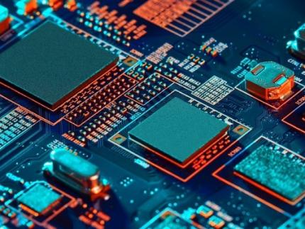 KAIST researchers developed a novel ultra-low power memory for neuromorphic computing
A team of Korean researchers is making headlines by developing a new memory device that can be used to replace existing memory or used in implementing neuromorphic computing for next-generation artificial intelligence hardware for its low processing costs and its ultra-low power consumption.
KAIST (President Kwang-Hyung Lee) announced on April 4th that Professor Shinhyun Choi's research team in the School of Electrical Engineering has developed a next-generation phase change memory* device featuring ultra-low-power consumption that can replace DRAM and NAND flash memory.
☞ Phase change memory: A memory device that stores and/or processes information by changing the crystalline states of materials to be amorphous or crystalline using heat, thereby changing its resistance state.
Existing phase change memory has the problems such as expensive fabrication process for making highly scaled device and requiring substantial amount of power for operation. To solve these problems, Professor Choi’s research team developed an ultra-low power phase change memory device by electrically forming a very small nanometer (nm) scale phase changeable filament without expensive fabrication processes. This new development has the groundbreaking advantage of not only having a very low processing cost but also of enabling operating with ultra-low power consumption.
DRAM, one of the most popularly used memory, is very fast, but has volatile characteristics in which data disappears when the power is turned off. NAND flash memory, a storage device, has relatively slow read/write speeds, but it has non-volatile characteristic that enables it to preserve the data even when the power is cut off.
Phase change memory, on the other hand, combines the advantages of both DRAM and NAND flash memory, offering high speed and non-volatile characteristics. For this reason, phase change memory is being highlighted as the next-generation memory that can replace existing memory, and is being actively researched as a memory technology or neuromorphic computing technology that mimics the human brain.
However, conventional phase change memory devices require a substantial amount of power to operate, making it difficult to make practical large-capacity memory products or realize a neuromorphic computing system. In order to maximize the thermal efficiency for memory device operation, previous research efforts focused on reducing the power consumption by shrinking the physical size of the device through the use of the state-of-the-art lithography technologies, but they were met with limitations in terms of practicality as the degree of improvement in power consumption was minimal whereas the cost and the difficulty of fabrication increased with each improvement.
In order to solve the power consumption problem of phase change memory, Professor Shinhyun Choi’s research team created a method to electrically form phase change materials in extremely small area, successfully implementing an ultra-low-power phase change memory device that consumes 15 times less power than a conventional phase change memory device fabricated with the expensive lithography tool.
< Figure 1. Illustrations of the ultra-low power phase change memory device developed through this study and the comparison of power consumption by the newly developed phase change memory device compared to conventional phase change memory devices. >
Professor Shinhyun Choi expressed strong confidence in how this research will span out in the future in the new field of research saying, "The phase change memory device we have developed is significant as it offers a novel approach to solve the lingering problems in producing a memory device at a greatly improved manufacturing cost and energy efficiency. We expect the results of our study to become the foundation of future electronic engineering, enabling various applications including high-density three-dimensional vertical memory and neuromorphic computing systems as it opened up the possibilities to choose from a variety of materials.” He went on to add, “I would like to thank the National Research Foundation of Korea and the National NanoFab Center for supporting this research.”
This study, in which See-On Park, a student of MS-PhD Integrated Program, and Seokman Hong, a doctoral student of the School of Electrical Engineering at KAIST, participated as first authors, was published on April 4 in the April issue of the renowned international academic journal Nature. (Paper title: Phase-Change Memory via a Phase-Changeable Self-Confined Nano-Filament)
This research was conducted with support from the Next-Generation Intelligent Semiconductor Technology Development Project, PIM AI Semiconductor Core Technology Development (Device) Project, Excellent Emerging Research Program of the National Research Foundation of Korea, and the Semiconductor Process-based Nanomedical Devices Development Project of the National NanoFab Center.
2024.04.04 View 9847
KAIST researchers developed a novel ultra-low power memory for neuromorphic computing
A team of Korean researchers is making headlines by developing a new memory device that can be used to replace existing memory or used in implementing neuromorphic computing for next-generation artificial intelligence hardware for its low processing costs and its ultra-low power consumption.
KAIST (President Kwang-Hyung Lee) announced on April 4th that Professor Shinhyun Choi's research team in the School of Electrical Engineering has developed a next-generation phase change memory* device featuring ultra-low-power consumption that can replace DRAM and NAND flash memory.
☞ Phase change memory: A memory device that stores and/or processes information by changing the crystalline states of materials to be amorphous or crystalline using heat, thereby changing its resistance state.
Existing phase change memory has the problems such as expensive fabrication process for making highly scaled device and requiring substantial amount of power for operation. To solve these problems, Professor Choi’s research team developed an ultra-low power phase change memory device by electrically forming a very small nanometer (nm) scale phase changeable filament without expensive fabrication processes. This new development has the groundbreaking advantage of not only having a very low processing cost but also of enabling operating with ultra-low power consumption.
DRAM, one of the most popularly used memory, is very fast, but has volatile characteristics in which data disappears when the power is turned off. NAND flash memory, a storage device, has relatively slow read/write speeds, but it has non-volatile characteristic that enables it to preserve the data even when the power is cut off.
Phase change memory, on the other hand, combines the advantages of both DRAM and NAND flash memory, offering high speed and non-volatile characteristics. For this reason, phase change memory is being highlighted as the next-generation memory that can replace existing memory, and is being actively researched as a memory technology or neuromorphic computing technology that mimics the human brain.
However, conventional phase change memory devices require a substantial amount of power to operate, making it difficult to make practical large-capacity memory products or realize a neuromorphic computing system. In order to maximize the thermal efficiency for memory device operation, previous research efforts focused on reducing the power consumption by shrinking the physical size of the device through the use of the state-of-the-art lithography technologies, but they were met with limitations in terms of practicality as the degree of improvement in power consumption was minimal whereas the cost and the difficulty of fabrication increased with each improvement.
In order to solve the power consumption problem of phase change memory, Professor Shinhyun Choi’s research team created a method to electrically form phase change materials in extremely small area, successfully implementing an ultra-low-power phase change memory device that consumes 15 times less power than a conventional phase change memory device fabricated with the expensive lithography tool.
< Figure 1. Illustrations of the ultra-low power phase change memory device developed through this study and the comparison of power consumption by the newly developed phase change memory device compared to conventional phase change memory devices. >
Professor Shinhyun Choi expressed strong confidence in how this research will span out in the future in the new field of research saying, "The phase change memory device we have developed is significant as it offers a novel approach to solve the lingering problems in producing a memory device at a greatly improved manufacturing cost and energy efficiency. We expect the results of our study to become the foundation of future electronic engineering, enabling various applications including high-density three-dimensional vertical memory and neuromorphic computing systems as it opened up the possibilities to choose from a variety of materials.” He went on to add, “I would like to thank the National Research Foundation of Korea and the National NanoFab Center for supporting this research.”
This study, in which See-On Park, a student of MS-PhD Integrated Program, and Seokman Hong, a doctoral student of the School of Electrical Engineering at KAIST, participated as first authors, was published on April 4 in the April issue of the renowned international academic journal Nature. (Paper title: Phase-Change Memory via a Phase-Changeable Self-Confined Nano-Filament)
This research was conducted with support from the Next-Generation Intelligent Semiconductor Technology Development Project, PIM AI Semiconductor Core Technology Development (Device) Project, Excellent Emerging Research Program of the National Research Foundation of Korea, and the Semiconductor Process-based Nanomedical Devices Development Project of the National NanoFab Center.
2024.04.04 View 9847 -
 KAIST Team Develops an Insect-Mimicking Semiconductor to Detect Motion
The recent development of an “intelligent sensor” semiconductor that mimics the optic nerve of insects while operating at ultra-high speeds and low power offers extensive expandability into various innovative technologies. This technology is expected to be applied to various fields including transportation, safety, and security systems, contributing to both industry and society.
On February 19, a KAIST research team led by Professor Kyung Min Kim from the Department of Materials Science and Engineering (DMSE) announced the successful developed an intelligent motion detector by merging various memristor* devices to mimic the visual intelligence** of the optic nerve of insects.
*Memristor: a “memory resistor” whose state of resistance changes depending on the input signal
**Visual intelligence: the ability to interpret visual information and perform calculations within the optic nerve
With the recent advances in AI technology, vision systems are being improved by utilizing AI in various tasks such as image recognition, object detection, and motion analysis. However, existing vision systems typically recognize objects and their behaviour from the received image signals using complex algorithms. This method requires a significant amount of data traffic and higher power consumption, making it difficult to apply in mobile or IoT devices.
Meanwhile, insects are known to be able to effectively process visual information through an optic nerve circuit called the elementary motion detector, allowing them to detect objects and recognize their motion at an advanced level. However, mimicking this pathway using conventional silicon integrated circuit (CMOS) technology requires complex circuits, and its implementation into actual devices has thus been limited.
< Figure 1. Working principle of a biological elementary motion detection system. >
Professor Kyung Min Kim’s research team developed an intelligent motion detecting sensor that operates at a high level of efficiency and ultra-high speeds. The device has a simple structure consisting of only two types of memristors and a resistor developed by the team. The two different memristors each carry out a signal delay function and a signal integration and ignition function, respectively. Through them, the team could directly mimic the optic nerve of insects to analyze object movement.
< Figure 2. (Left) Optical image of the M-EMD device in the left panel (scale bar 200 μm) and SEM image of the device in the right panel (scale bar: 20 μm). (Middle) Responses of the M-EMD in positive direction. (Right) Responses of the M-EMD in negative direction. >
To demonstrate its potential for practical applications, the research team used the newly developed motion detector to design a neuromorphic computing system that can predict the path of a vehicle. The results showed that the device used 92.9% less energy compared to existing technology and predicted motion with more accuracy.
< Figure 3. Neuromorphic computing system configuration based on motion recognition devices >
Professor Kim said, “Insects make use of their very simple visual intelligence systems to detect the motion of objects at a surprising high speed. This research is significant in that we could mimic the functions of a nerve using a memristor device.” He added, “Edge AI devices, such as AI-topped mobile phones, are becoming increasingly important. This research can contribute to the integration of efficient vision systems for motion recognition, so we expect it to be applied to various fields such as autonomous vehicles, vehicle transportation systems, robotics, and machine vision.”
This research, conducted by co-first authors Hanchan Song and Min Gu Lee, both Ph.D. candidates at KAIST DMSE, was published in the online issue of Advanced Materials on January 29.
This research was supported by the Mid-Sized Research Project by the National Research Foundation of Korea, the Next-Generation Intelligent Semiconductor Technology Development Project, the PIM Artificial Intelligence Semiconductor Core Technology Development Project, the National Nano Fab Center, and the Leap Research Project by KAIST.
2024.02.29 View 9240
KAIST Team Develops an Insect-Mimicking Semiconductor to Detect Motion
The recent development of an “intelligent sensor” semiconductor that mimics the optic nerve of insects while operating at ultra-high speeds and low power offers extensive expandability into various innovative technologies. This technology is expected to be applied to various fields including transportation, safety, and security systems, contributing to both industry and society.
On February 19, a KAIST research team led by Professor Kyung Min Kim from the Department of Materials Science and Engineering (DMSE) announced the successful developed an intelligent motion detector by merging various memristor* devices to mimic the visual intelligence** of the optic nerve of insects.
*Memristor: a “memory resistor” whose state of resistance changes depending on the input signal
**Visual intelligence: the ability to interpret visual information and perform calculations within the optic nerve
With the recent advances in AI technology, vision systems are being improved by utilizing AI in various tasks such as image recognition, object detection, and motion analysis. However, existing vision systems typically recognize objects and their behaviour from the received image signals using complex algorithms. This method requires a significant amount of data traffic and higher power consumption, making it difficult to apply in mobile or IoT devices.
Meanwhile, insects are known to be able to effectively process visual information through an optic nerve circuit called the elementary motion detector, allowing them to detect objects and recognize their motion at an advanced level. However, mimicking this pathway using conventional silicon integrated circuit (CMOS) technology requires complex circuits, and its implementation into actual devices has thus been limited.
< Figure 1. Working principle of a biological elementary motion detection system. >
Professor Kyung Min Kim’s research team developed an intelligent motion detecting sensor that operates at a high level of efficiency and ultra-high speeds. The device has a simple structure consisting of only two types of memristors and a resistor developed by the team. The two different memristors each carry out a signal delay function and a signal integration and ignition function, respectively. Through them, the team could directly mimic the optic nerve of insects to analyze object movement.
< Figure 2. (Left) Optical image of the M-EMD device in the left panel (scale bar 200 μm) and SEM image of the device in the right panel (scale bar: 20 μm). (Middle) Responses of the M-EMD in positive direction. (Right) Responses of the M-EMD in negative direction. >
To demonstrate its potential for practical applications, the research team used the newly developed motion detector to design a neuromorphic computing system that can predict the path of a vehicle. The results showed that the device used 92.9% less energy compared to existing technology and predicted motion with more accuracy.
< Figure 3. Neuromorphic computing system configuration based on motion recognition devices >
Professor Kim said, “Insects make use of their very simple visual intelligence systems to detect the motion of objects at a surprising high speed. This research is significant in that we could mimic the functions of a nerve using a memristor device.” He added, “Edge AI devices, such as AI-topped mobile phones, are becoming increasingly important. This research can contribute to the integration of efficient vision systems for motion recognition, so we expect it to be applied to various fields such as autonomous vehicles, vehicle transportation systems, robotics, and machine vision.”
This research, conducted by co-first authors Hanchan Song and Min Gu Lee, both Ph.D. candidates at KAIST DMSE, was published in the online issue of Advanced Materials on January 29.
This research was supported by the Mid-Sized Research Project by the National Research Foundation of Korea, the Next-Generation Intelligent Semiconductor Technology Development Project, the PIM Artificial Intelligence Semiconductor Core Technology Development Project, the National Nano Fab Center, and the Leap Research Project by KAIST.
2024.02.29 View 9240 -
 A KAIST Research Team Develops an Ultra-High Performing “Universal Electrode” for Next-Generation Fuel Cells
Fuel cells are devices that generate electricity with high efficiency using hydrogen, a clean energy source, and are expected to play an important part in the upcoming hydrogen society. The recent development of an excellent universal electrode material that is applicable to all next-generation fuel cells and can withstand 700 hours of operation has therefore garnered a great deal of attention.
On August 9, a joint research team led by Prof. WooChul Jung from the KAIST Department of Materials Science and Engineering, Prof. Kang Taek Lee from the KAIST Department of Mechanical Engineering, and Prof. Jun Hyuk Kim from the Department of Chemical Engineering at Hongik University announced the development of an electrode material that is applicable to both oxygen- and proton-conducting solid oxide cells.
Depending on the type of ion conducted by the electrolyte, ceramic fuel cells are categorized into either solid oxide fuel cells (SOFC) or protonic ceramic fuel cells (PCFC). As they can both convert between electricity and hydrogen production, fuel cells can be categorized into a total of four device types. These devices are applicable in hydrogen fuel cell vehicles, hydrogen charging stations, and power generation systems, and are henceforth emerging as core next-generation technologies for a carbon-neutral society.
However, these devices have a chronic problem where the speed of their slowest reaction would decrease with a drop of driving temperature, which greatly reduces device efficiency. Various studies have been conducted to solve this, but most reported that electrode materials have low catalytic activity and their applications are limited to specific devices, which limits them from being used as SOFCs that require reversible power conversion and hydrogen production.
< Figure 1. Schematic diagram of high-performance oxygen ion conductive solid oxide fuel cell (SOFC) and proton conductive ceramic fuel cell (PCFC) operates with the new universal electrodes >
To solve this issue, the research team doped a perovskite oxide material with Ta5+, a high valence ion that did not receive much attention in the field. Through this, the team successfully stabilized what is usually a highly unstable crystal structure, and confirmed that catalytic activity improved by 100 times.
The electrode material developed by the team was applied to all four of the mentioned device types. Furthermore, their efficiencies were greater than any of the devices reported thus far, and showed excellent performance by stably running for much longer (700 hours) compared to existing materials that deteriorated within the first 100 hours of operation.
< Figure 2. (a) Power conversion and hydrogen production performance chart for the protonic ceramic fuel cell (PCFC) with the new universal electrodes (b) and performance comparison with other reported devices >
This research, in which KAIST’s Ph.D. candidates Dongyeon Kim and Sejong Ahn, and Professor Jun Hyuk Kim from Hongik University contributed as co-first authors, was published in the internationally renowned Energy & Environmental Science under the title, "Oxygen-Electrode for Reversible Solid Oxide Electrochemical Cells at Reduced Temperatures".
Prof. WooChul Jung said, “We broke free from the idea that we must develop a completely new material to solve an existing problem, and instead suggested a way to control the crystal structure of a lesser-known material to develop a high-efficiency fuel cell, and that’s what makes these results more significant.”
Prof. Kang Taek Lee added, “Unlike previously reported materials that could only be applied to one device type at a time, our material has the flexibility of being applicable to all four. We therefore look forward to its contribution in the commercialization of eco-friendly energy technology including fuel cells and water-splitting equipment for hydrogen production.”
This research was supported by a National Research Foundation of Korea (NRF) grant funded by the Korean Ministry of Science and ICT.
2023.08.22 View 10126
A KAIST Research Team Develops an Ultra-High Performing “Universal Electrode” for Next-Generation Fuel Cells
Fuel cells are devices that generate electricity with high efficiency using hydrogen, a clean energy source, and are expected to play an important part in the upcoming hydrogen society. The recent development of an excellent universal electrode material that is applicable to all next-generation fuel cells and can withstand 700 hours of operation has therefore garnered a great deal of attention.
On August 9, a joint research team led by Prof. WooChul Jung from the KAIST Department of Materials Science and Engineering, Prof. Kang Taek Lee from the KAIST Department of Mechanical Engineering, and Prof. Jun Hyuk Kim from the Department of Chemical Engineering at Hongik University announced the development of an electrode material that is applicable to both oxygen- and proton-conducting solid oxide cells.
Depending on the type of ion conducted by the electrolyte, ceramic fuel cells are categorized into either solid oxide fuel cells (SOFC) or protonic ceramic fuel cells (PCFC). As they can both convert between electricity and hydrogen production, fuel cells can be categorized into a total of four device types. These devices are applicable in hydrogen fuel cell vehicles, hydrogen charging stations, and power generation systems, and are henceforth emerging as core next-generation technologies for a carbon-neutral society.
However, these devices have a chronic problem where the speed of their slowest reaction would decrease with a drop of driving temperature, which greatly reduces device efficiency. Various studies have been conducted to solve this, but most reported that electrode materials have low catalytic activity and their applications are limited to specific devices, which limits them from being used as SOFCs that require reversible power conversion and hydrogen production.
< Figure 1. Schematic diagram of high-performance oxygen ion conductive solid oxide fuel cell (SOFC) and proton conductive ceramic fuel cell (PCFC) operates with the new universal electrodes >
To solve this issue, the research team doped a perovskite oxide material with Ta5+, a high valence ion that did not receive much attention in the field. Through this, the team successfully stabilized what is usually a highly unstable crystal structure, and confirmed that catalytic activity improved by 100 times.
The electrode material developed by the team was applied to all four of the mentioned device types. Furthermore, their efficiencies were greater than any of the devices reported thus far, and showed excellent performance by stably running for much longer (700 hours) compared to existing materials that deteriorated within the first 100 hours of operation.
< Figure 2. (a) Power conversion and hydrogen production performance chart for the protonic ceramic fuel cell (PCFC) with the new universal electrodes (b) and performance comparison with other reported devices >
This research, in which KAIST’s Ph.D. candidates Dongyeon Kim and Sejong Ahn, and Professor Jun Hyuk Kim from Hongik University contributed as co-first authors, was published in the internationally renowned Energy & Environmental Science under the title, "Oxygen-Electrode for Reversible Solid Oxide Electrochemical Cells at Reduced Temperatures".
Prof. WooChul Jung said, “We broke free from the idea that we must develop a completely new material to solve an existing problem, and instead suggested a way to control the crystal structure of a lesser-known material to develop a high-efficiency fuel cell, and that’s what makes these results more significant.”
Prof. Kang Taek Lee added, “Unlike previously reported materials that could only be applied to one device type at a time, our material has the flexibility of being applicable to all four. We therefore look forward to its contribution in the commercialization of eco-friendly energy technology including fuel cells and water-splitting equipment for hydrogen production.”
This research was supported by a National Research Foundation of Korea (NRF) grant funded by the Korean Ministry of Science and ICT.
2023.08.22 View 10126 -
 “3D sketch” Your Ideas and Bring Them to Life, Instantly!
Professor Seok-Hyung Bae’s research team at the Department of Industrial Design developed a novel 3D sketching system that rapidly creates animated 3D concepts through simple user interactions like sketching on a piece of paper or playing a toy.
Foldable drones, transforming vehicles, and multi-legged robots from sci-fi movies are now becoming commonplace thanks to technological progress. However, designing them remains a difficult challenge even for skilled experts, because complex design decisions must be made regarding not only their form, but also the structure, poses, and motions, which are interdependent on one another.
Creating a 3D concept comprising of multiple moving parts connected by different types of joints using a traditional 3D CAD tool, which is more suited for processing precise and elaborate modeling, is a painstaking and time-consuming process. This presents a major bottleneck for the workflow during the early stage of design, in which it is preferred that as many ideas are tried and discarded out as quickly as possible in order to explore a wide range of possibilities in the shortest amount of time.
A research team led by Professor Bae has focused on designers’ freehand sketches drew up with a pen on a paper that serve as the starting point for virtually all design projects. This led them to develop their 3D sketching technology to generate desired 3D curves from the rough but expressive 2D strokes drawn with a digital stylus on a digital tablet.
Their latest research helps designers bring their 3D sketches to life almost instantly. Using the intuitive set of multi-touch gestures the team successfully designed and implemented, designers can handle the 3D sketches they are working on with their fingers as if they are playing with toys and put them into animation in no time.
< Figure 1. A novel 3D sketching system for rapidly designing articulated 3D concepts with a small set of coherent pen and multi-touch gestures. (a) Sketching: A 3D sketch curve is created by marking a pen stroke that is projected onto a sketch plane widget. (b) Segmenting: Entire or partial sketch curves are added to separate parts that serve as links in the kinematic chain. (c) Rigging: Repeatedly demonstrating the desired motion of a part leaves behind a trail, from which the system infers a joint. (d) Posing: Desired poses can be achieved through actuating joints via forward or inverse kinematics. (e) Filming: A sequence of keyframes specifying desired poses and viewpoints is connected as a smooth motion. >
< Figure 2. (a) Concept drawing of an autonomous excavator. It features (b, c) four caterpillars that swivel for high maneuverability, (d) an extendable boom and a bucket connected by multiple links, and (e) a rotating platform. The concept’s designer, who had 8 years of work experience, estimated that it would take 1-2 weeks to express and communicate such a complex articulated object with existing tools. With the proposed system, it took only 2 hours and 52 minutes. >
The major findings of their work were published under the title “Rapid Design of Articulated Objects” in ACM Transactions on Graphics (impact factor: 7.403), the top international journal in the field of computer graphics, and presented at ACM SIGGRAPH 2022 (h5-index: 103), the world’s largest international academic conference in the field, which was held back in August in Vancouver, Canada with Joon Hyub Lee, a Ph.D. student of the Department of Industrial Design as the first author.
The ACM SIGGRAPH 2022 conference was reportedly attended by over 10,000 participants including researchers, artists, and developers from world-renowned universities; film, animation, and game studies, such as Marvel, Pixar, and Blizzard; high-tech manufacturers, such as Lockheed Martin and Boston Dynamics; and metaverse platform companies, such as Meta and Roblox.
< Figure 3. The findings of Professor Bae’s research team were published in ACM Transactions on Graphics, the top international academic journal in the field of computer graphics, and presented at ACM SIGGRAPH 2022, the largest international academic conference held in conjunction early August in Vancouver, Canada. The team’s live demo at the Emerging Technologies program was highly praised by numerous academics and industry officials and received an Honorable Mention. >
The team was also invited to present their technical paper as a demo and a special talk at the Emerging Technologies program at ACM SIGGRAPH 2022 as one of the top-three impactful technologies. The live performance, in which Hanbit Kim, a Ph.D. student of the Department of Industrial Design at KAIST and a co-author, sketched and animated a sophisticated animal-shaped robot from scratch in a matter of a few minutes, wowed the audience and won the Honorable Mention Award from the jury.
Edwin Catmull, the co-founder of Pixar and a keynote speaker at the SIGGRAPH conference, praised the team’s research on 3D sketching as “really excellent work” and “a kind of tool that would be useful to Pixar's creative model designers.”
This technology, which became virally popular in Japan after featuring in an online IT media outlet and attracting more than 600K views, received a special award from the Digital Content Association of Japan (DCAJ) and was invited and exhibited for three days at Tokyo in November, as a part of Inter BEE 2022, the largest broadcasting and media expo in Japan.
“The more we come to understand how designers think and work, the more effective design tools can be built around that understanding,” said Professor Bae, explaining that “the key is to integrate different algorithms into a harmonious system as intuitive interactions.” He added that “this work wouldn’t have been possible if it weren’t for the convergent research environment cultivated by the Department of Industrial Design at KAIST, in which all students see themselves not only as aspiring creative designers, but also as practical engineers.”
By enabling designers to produce highly expressive animated 3D concepts far more quickly and easily in comparison to using existing methods, this new tool is expected to revolutionize design practices and processes in the content creation, manufacturing, and metaverse-related industries.
This research was funded by the Ministry of Science and ICT, and the National Research Foundation of Korea.
More info: https://sketch.kaist.ac.kr/publications/2022_siggraph_rapid_design
Video: https://www.youtube.com/watch?v=rsBl0QvSDqI
< Figure 4. From left to right: Ph.D. students Hanbit Kim, and Joon Hyub Lee and Professor Bae of the Department of Industrial Design, KAIST >
2022.11.23 View 13156
“3D sketch” Your Ideas and Bring Them to Life, Instantly!
Professor Seok-Hyung Bae’s research team at the Department of Industrial Design developed a novel 3D sketching system that rapidly creates animated 3D concepts through simple user interactions like sketching on a piece of paper or playing a toy.
Foldable drones, transforming vehicles, and multi-legged robots from sci-fi movies are now becoming commonplace thanks to technological progress. However, designing them remains a difficult challenge even for skilled experts, because complex design decisions must be made regarding not only their form, but also the structure, poses, and motions, which are interdependent on one another.
Creating a 3D concept comprising of multiple moving parts connected by different types of joints using a traditional 3D CAD tool, which is more suited for processing precise and elaborate modeling, is a painstaking and time-consuming process. This presents a major bottleneck for the workflow during the early stage of design, in which it is preferred that as many ideas are tried and discarded out as quickly as possible in order to explore a wide range of possibilities in the shortest amount of time.
A research team led by Professor Bae has focused on designers’ freehand sketches drew up with a pen on a paper that serve as the starting point for virtually all design projects. This led them to develop their 3D sketching technology to generate desired 3D curves from the rough but expressive 2D strokes drawn with a digital stylus on a digital tablet.
Their latest research helps designers bring their 3D sketches to life almost instantly. Using the intuitive set of multi-touch gestures the team successfully designed and implemented, designers can handle the 3D sketches they are working on with their fingers as if they are playing with toys and put them into animation in no time.
< Figure 1. A novel 3D sketching system for rapidly designing articulated 3D concepts with a small set of coherent pen and multi-touch gestures. (a) Sketching: A 3D sketch curve is created by marking a pen stroke that is projected onto a sketch plane widget. (b) Segmenting: Entire or partial sketch curves are added to separate parts that serve as links in the kinematic chain. (c) Rigging: Repeatedly demonstrating the desired motion of a part leaves behind a trail, from which the system infers a joint. (d) Posing: Desired poses can be achieved through actuating joints via forward or inverse kinematics. (e) Filming: A sequence of keyframes specifying desired poses and viewpoints is connected as a smooth motion. >
< Figure 2. (a) Concept drawing of an autonomous excavator. It features (b, c) four caterpillars that swivel for high maneuverability, (d) an extendable boom and a bucket connected by multiple links, and (e) a rotating platform. The concept’s designer, who had 8 years of work experience, estimated that it would take 1-2 weeks to express and communicate such a complex articulated object with existing tools. With the proposed system, it took only 2 hours and 52 minutes. >
The major findings of their work were published under the title “Rapid Design of Articulated Objects” in ACM Transactions on Graphics (impact factor: 7.403), the top international journal in the field of computer graphics, and presented at ACM SIGGRAPH 2022 (h5-index: 103), the world’s largest international academic conference in the field, which was held back in August in Vancouver, Canada with Joon Hyub Lee, a Ph.D. student of the Department of Industrial Design as the first author.
The ACM SIGGRAPH 2022 conference was reportedly attended by over 10,000 participants including researchers, artists, and developers from world-renowned universities; film, animation, and game studies, such as Marvel, Pixar, and Blizzard; high-tech manufacturers, such as Lockheed Martin and Boston Dynamics; and metaverse platform companies, such as Meta and Roblox.
< Figure 3. The findings of Professor Bae’s research team were published in ACM Transactions on Graphics, the top international academic journal in the field of computer graphics, and presented at ACM SIGGRAPH 2022, the largest international academic conference held in conjunction early August in Vancouver, Canada. The team’s live demo at the Emerging Technologies program was highly praised by numerous academics and industry officials and received an Honorable Mention. >
The team was also invited to present their technical paper as a demo and a special talk at the Emerging Technologies program at ACM SIGGRAPH 2022 as one of the top-three impactful technologies. The live performance, in which Hanbit Kim, a Ph.D. student of the Department of Industrial Design at KAIST and a co-author, sketched and animated a sophisticated animal-shaped robot from scratch in a matter of a few minutes, wowed the audience and won the Honorable Mention Award from the jury.
Edwin Catmull, the co-founder of Pixar and a keynote speaker at the SIGGRAPH conference, praised the team’s research on 3D sketching as “really excellent work” and “a kind of tool that would be useful to Pixar's creative model designers.”
This technology, which became virally popular in Japan after featuring in an online IT media outlet and attracting more than 600K views, received a special award from the Digital Content Association of Japan (DCAJ) and was invited and exhibited for three days at Tokyo in November, as a part of Inter BEE 2022, the largest broadcasting and media expo in Japan.
“The more we come to understand how designers think and work, the more effective design tools can be built around that understanding,” said Professor Bae, explaining that “the key is to integrate different algorithms into a harmonious system as intuitive interactions.” He added that “this work wouldn’t have been possible if it weren’t for the convergent research environment cultivated by the Department of Industrial Design at KAIST, in which all students see themselves not only as aspiring creative designers, but also as practical engineers.”
By enabling designers to produce highly expressive animated 3D concepts far more quickly and easily in comparison to using existing methods, this new tool is expected to revolutionize design practices and processes in the content creation, manufacturing, and metaverse-related industries.
This research was funded by the Ministry of Science and ICT, and the National Research Foundation of Korea.
More info: https://sketch.kaist.ac.kr/publications/2022_siggraph_rapid_design
Video: https://www.youtube.com/watch?v=rsBl0QvSDqI
< Figure 4. From left to right: Ph.D. students Hanbit Kim, and Joon Hyub Lee and Professor Bae of the Department of Industrial Design, KAIST >
2022.11.23 View 13156