KRISS
-
 KAIST's Li-Fi - Achieves 100 Times Faster Speed and Enhanced Security of Wi-Fi
- KAIST-KRISS Develop 'On-Device Encryption Optical Transmitter' Based on Eco-Friendly Quantum Dots
- New Li-Fi Platform Technology Achieves High Performance with 17.4% Device Efficiency and 29,000 nit Brightness, Simultaneously Improving Transmission Speed and Security
- Presents New Methodology for High-Speed and Encrypted Communication Through Single-Device-Based Dual-Channel Optical Modulation
< Photo 1. (Front row from left) Seungmin Shin, First Author; Professor Himchan Cho; (Back row from left) Hyungdoh Lee, Seungwoo Lee, Wonbeom Lee; (Top left) Dr. Kyung-geun Lim >
Li-Fi (Light Fidelity) is a wireless communication technology that utilizes the visible light spectrum (400-800 THz), similar to LED light, offering speeds up to 100 times faster than existing Wi-Fi (up to 224 Gbps). While it has fewer limitations in available frequency allocation and less radio interference, it is relatively vulnerable to security breaches as anyone can access it. Korean researchers have now proposed a new Li-Fi platform that overcomes the limitations of conventional optical communication devices and can simultaneously enhance both transmission speed and security.
KAIST (President Kwang Hyung Lee) announced on the 24th that Professor Himchan Cho's research team from the Department of Materials Science and Engineering, in collaboration with Dr. Kyung-geun Lim of the Korea Research Institute of Standards and Science (KRISS, President Ho-Seong Lee) under the National Research Council of Science & Technology (NST, Chairman Young-Sik Kim), has developed 'on-device encryption optical communication device' technology for the utilization of 'Li-Fi,' which is attracting attention as a next-generation ultra-high-speed data communication.
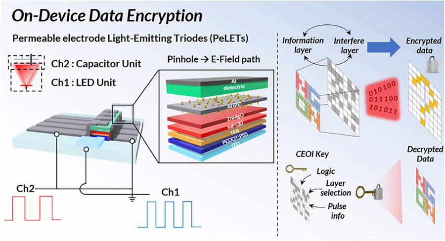
Professor Cho's team created high-efficiency light-emitting triode devices using eco-friendly quantum dots (low-toxicity and sustainable materials). The device developed by the research team is a mechanism that generates light using an electric field. Specifically, the electric field is concentrated in 'tiny holes (pinholes) in the permeable electrode' and transmitted beyond the electrode. This device utilizes this principle to simultaneously process two input data streams.
Using this principle, the research team developed a technology called 'on-device encryption optical transmitter.' The core of this technology is that the device itself converts information into light and simultaneously encrypts it. This means that enhanced security data transmission is possible without the need for complex, separate equipment.
External Quantum Efficiency (EQE) is an indicator of how efficiently electricity is converted into light, with a general commercialization standard of about 20%. The newly developed device recorded an EQE of 17.4%, and its luminance was 29,000 nit, significantly exceeding the maximum brightness of a smartphone OLED screen, which is 2,000 nit, demonstrating a brightness more than 10 times higher.
< Figure 1. Schematic diagram of the device structure developed by the research team and encrypted communication >
Furthermore, to more accurately understand how this device converts information into light, the research team used a method called 'transient electroluminescence analysis.' They analyzed the light-emitting characteristics generated by the device when voltage was instantaneously applied for very short durations (hundreds of nanoseconds = billionths of a second). Through this analysis, they investigated the movement of charges within the device at hundreds of nanoseconds, elucidating the operating mechanism of dual-channel optical modulation implemented within a single device.
Professor Himchan Cho of KAIST stated, "This research overcomes the limitations of existing optical communication devices and proposes a new communication platform that can both increase transmission speed and enhance security."
< Photo 2. Professor Himchan Cho, Department of Materials Science and Engineering >
He added, "This technology, which strengthens security without additional equipment and simultaneously enables encryption and transmission, can be widely applied in various fields where security is crucial in the future."
This research, with Seungmin Shin, a Ph.D. candidate at KAIST's Department of Materials Science and Engineering, participating as the first author, and Professor Himchan Cho and Dr. Kyung-geun Lim of KRISS as co-corresponding authors, was published in the international journal 'Advanced Materials' on May 30th and was selected as an inside front cover paper.※ Paper Title: High-Efficiency Quantum Dot Permeable electrode Light-Emitting Triodes for Visible-Light Communications and On-Device Data Encryption※ DOI: https://doi.org/10.1002/adma.202503189
This research was supported by the National Research Foundation of Korea, the National Research Council of Science & Technology (NST), and the Korea Institute for Advancement of Technology.
2025.06.24 View 329
KAIST's Li-Fi - Achieves 100 Times Faster Speed and Enhanced Security of Wi-Fi
- KAIST-KRISS Develop 'On-Device Encryption Optical Transmitter' Based on Eco-Friendly Quantum Dots
- New Li-Fi Platform Technology Achieves High Performance with 17.4% Device Efficiency and 29,000 nit Brightness, Simultaneously Improving Transmission Speed and Security
- Presents New Methodology for High-Speed and Encrypted Communication Through Single-Device-Based Dual-Channel Optical Modulation
< Photo 1. (Front row from left) Seungmin Shin, First Author; Professor Himchan Cho; (Back row from left) Hyungdoh Lee, Seungwoo Lee, Wonbeom Lee; (Top left) Dr. Kyung-geun Lim >
Li-Fi (Light Fidelity) is a wireless communication technology that utilizes the visible light spectrum (400-800 THz), similar to LED light, offering speeds up to 100 times faster than existing Wi-Fi (up to 224 Gbps). While it has fewer limitations in available frequency allocation and less radio interference, it is relatively vulnerable to security breaches as anyone can access it. Korean researchers have now proposed a new Li-Fi platform that overcomes the limitations of conventional optical communication devices and can simultaneously enhance both transmission speed and security.
KAIST (President Kwang Hyung Lee) announced on the 24th that Professor Himchan Cho's research team from the Department of Materials Science and Engineering, in collaboration with Dr. Kyung-geun Lim of the Korea Research Institute of Standards and Science (KRISS, President Ho-Seong Lee) under the National Research Council of Science & Technology (NST, Chairman Young-Sik Kim), has developed 'on-device encryption optical communication device' technology for the utilization of 'Li-Fi,' which is attracting attention as a next-generation ultra-high-speed data communication.
Professor Cho's team created high-efficiency light-emitting triode devices using eco-friendly quantum dots (low-toxicity and sustainable materials). The device developed by the research team is a mechanism that generates light using an electric field. Specifically, the electric field is concentrated in 'tiny holes (pinholes) in the permeable electrode' and transmitted beyond the electrode. This device utilizes this principle to simultaneously process two input data streams.
Using this principle, the research team developed a technology called 'on-device encryption optical transmitter.' The core of this technology is that the device itself converts information into light and simultaneously encrypts it. This means that enhanced security data transmission is possible without the need for complex, separate equipment.
External Quantum Efficiency (EQE) is an indicator of how efficiently electricity is converted into light, with a general commercialization standard of about 20%. The newly developed device recorded an EQE of 17.4%, and its luminance was 29,000 nit, significantly exceeding the maximum brightness of a smartphone OLED screen, which is 2,000 nit, demonstrating a brightness more than 10 times higher.
< Figure 1. Schematic diagram of the device structure developed by the research team and encrypted communication >
Furthermore, to more accurately understand how this device converts information into light, the research team used a method called 'transient electroluminescence analysis.' They analyzed the light-emitting characteristics generated by the device when voltage was instantaneously applied for very short durations (hundreds of nanoseconds = billionths of a second). Through this analysis, they investigated the movement of charges within the device at hundreds of nanoseconds, elucidating the operating mechanism of dual-channel optical modulation implemented within a single device.
Professor Himchan Cho of KAIST stated, "This research overcomes the limitations of existing optical communication devices and proposes a new communication platform that can both increase transmission speed and enhance security."
< Photo 2. Professor Himchan Cho, Department of Materials Science and Engineering >
He added, "This technology, which strengthens security without additional equipment and simultaneously enables encryption and transmission, can be widely applied in various fields where security is crucial in the future."
This research, with Seungmin Shin, a Ph.D. candidate at KAIST's Department of Materials Science and Engineering, participating as the first author, and Professor Himchan Cho and Dr. Kyung-geun Lim of KRISS as co-corresponding authors, was published in the international journal 'Advanced Materials' on May 30th and was selected as an inside front cover paper.※ Paper Title: High-Efficiency Quantum Dot Permeable electrode Light-Emitting Triodes for Visible-Light Communications and On-Device Data Encryption※ DOI: https://doi.org/10.1002/adma.202503189
This research was supported by the National Research Foundation of Korea, the National Research Council of Science & Technology (NST), and the Korea Institute for Advancement of Technology.
2025.06.24 View 329 -
 An Electron Cloud Distribution Observed by the Scanning Seebeck Microscope
All matters are made of small particles, namely atoms. An atom is composed of a heavy nucleus and cloud-like, extremely light electrons.
Korean researchers developed an electron microscopy technique that enables the accurate observation of an electron cloud distribution at room-temperature. The achievement is comparable to the invention of the quantum tunneling microscopy technique developed 33 years ago.
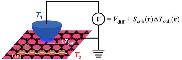
Professor Yong-Hyun Kim of the Graduate School of Nanoscience and Technology at KAIST and Dr. Ho-Gi Yeo of the Korea Research Institute of Standards and Science (KRISS) developed the Scanning Seebeck Microscope (SSM). The SSM renders clear images of atoms, as well as an electron cloud distribution. This was achieved by creating a voltage difference via a temperature gradient.
The development was introduced in the online edition of Physical Review Letters (April 2014), a prestigious journal published by the American Institute of Physics.
The SSM is expected to be economically competitive as it gives high resolution images at an atomic scale even for graphene and semiconductors, both at room temperature. In addition, if the SSM is applied to thermoelectric material research, it will contribute to the development of high-efficiency thermoelectric materials.
Through numerous hypotheses and experiments, scientists now believe that there exists an electron cloud surrounding a nucleus. IBM's Scanning Tunneling Microscope (STM) was the first to observe the electron cloud and has remained as the only technique to this day. The developers of IBM microscope, Dr. Gerd Binnig and Dr. Heinrich Rohrer, were awarded the 1986 Nobel Prize in Physics.
There still remains a downside to the STM technique, however: it required high precision and extreme low temperature and vibration. The application of voltage also affects the electron cloud, resulting in a distorted image.
The KAIST research team adopted a different approach by using the Seebeck effect which refers to the voltage generation due to a temperature gradient between two materials.
The team placed an observation sample (graphene) at room temperature (37~57℃) and detected its voltage generation. This technique made it possible to observe an electron cloud at room temperature.
Furthermore, the research team investigated the theoretical quantum mechanics behind the electron cloud using the observation gained through the Seebeck effect and also obtained by simulation capability to analyze the experimental results.
The research was a joint research project between KAIST Professor Yong-Hyun Kim and KRISS researcher Dr. Ho-Gi Yeo. Eui-Seop Lee, a Ph.D. candidate of KAIST, and KRISS researcher Dr. Sang-Hui Cho also participated. The Ministry of Science, ICT, and Future Planning, the Global Frontier Initiative, and the Disruptive Convergent Technology Development Initiative funded the project in Korea.
Picture 1: Schematic Diagram of the Scanning Seebeck Microscope (SSM)
Picture 2: Electron cloud distribution observed by SSM at room temperature
Picture 3: Professor Yong-Hyun Kim
2014.04.04 View 16298
An Electron Cloud Distribution Observed by the Scanning Seebeck Microscope
All matters are made of small particles, namely atoms. An atom is composed of a heavy nucleus and cloud-like, extremely light electrons.
Korean researchers developed an electron microscopy technique that enables the accurate observation of an electron cloud distribution at room-temperature. The achievement is comparable to the invention of the quantum tunneling microscopy technique developed 33 years ago.
Professor Yong-Hyun Kim of the Graduate School of Nanoscience and Technology at KAIST and Dr. Ho-Gi Yeo of the Korea Research Institute of Standards and Science (KRISS) developed the Scanning Seebeck Microscope (SSM). The SSM renders clear images of atoms, as well as an electron cloud distribution. This was achieved by creating a voltage difference via a temperature gradient.
The development was introduced in the online edition of Physical Review Letters (April 2014), a prestigious journal published by the American Institute of Physics.
The SSM is expected to be economically competitive as it gives high resolution images at an atomic scale even for graphene and semiconductors, both at room temperature. In addition, if the SSM is applied to thermoelectric material research, it will contribute to the development of high-efficiency thermoelectric materials.
Through numerous hypotheses and experiments, scientists now believe that there exists an electron cloud surrounding a nucleus. IBM's Scanning Tunneling Microscope (STM) was the first to observe the electron cloud and has remained as the only technique to this day. The developers of IBM microscope, Dr. Gerd Binnig and Dr. Heinrich Rohrer, were awarded the 1986 Nobel Prize in Physics.
There still remains a downside to the STM technique, however: it required high precision and extreme low temperature and vibration. The application of voltage also affects the electron cloud, resulting in a distorted image.
The KAIST research team adopted a different approach by using the Seebeck effect which refers to the voltage generation due to a temperature gradient between two materials.
The team placed an observation sample (graphene) at room temperature (37~57℃) and detected its voltage generation. This technique made it possible to observe an electron cloud at room temperature.
Furthermore, the research team investigated the theoretical quantum mechanics behind the electron cloud using the observation gained through the Seebeck effect and also obtained by simulation capability to analyze the experimental results.
The research was a joint research project between KAIST Professor Yong-Hyun Kim and KRISS researcher Dr. Ho-Gi Yeo. Eui-Seop Lee, a Ph.D. candidate of KAIST, and KRISS researcher Dr. Sang-Hui Cho also participated. The Ministry of Science, ICT, and Future Planning, the Global Frontier Initiative, and the Disruptive Convergent Technology Development Initiative funded the project in Korea.
Picture 1: Schematic Diagram of the Scanning Seebeck Microscope (SSM)
Picture 2: Electron cloud distribution observed by SSM at room temperature
Picture 3: Professor Yong-Hyun Kim
2014.04.04 View 16298 -
 OLEV Safety Confirmed by International Standards
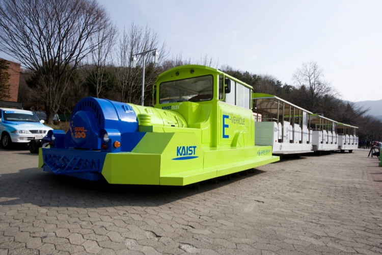
On September 19, KAIST announced that the electromagnetic (EM) field levels of its online electric vehicle (OLEV) measured in June and September of this year demonstrated verification of its safety.
Last June, the EM field level of OLEV installed at the Seoul Grand Park was measured by the Korea Research Institute of Standards and Science (KRISS) to test its harmfulness to human. The results were 0.5 ~ 61mG which is within the national and international standards of 62.5mG.
KRISS measured EM field levels on 22 spots on the side of and at the center of OLEV at a fixed distance (30cm) but variable heights (5cm~150cm) according to the national standard of measurement methods for electromagnetic fields of household appliances and similar apparatuses with regard to human exposure (IEC 62233).
In addition, another testing took place on September 13 following a request by National Assemblywoman Young-Ah Park, a member of the National Assembly’s Education, Science and Technology Committee, who has raised an issue on the safety of OLEV. This testing session was held by EMF Safety, Inc., an institution designated by Park, and it tested the EM field level of the same OLEV train that was tested in June.
As a result, the September measurements were well within the national and international standards with 0~24.1mG. The test was conducted under the presence of third party to produce a fair and objective result.
As reference, the EM field level results are well within the American IEEE electromagnetic field standards of 1,100 mG.
The September measurements were produced by Park’s recommendation of following the criteria specified in the measurement procedures of IEC 62110, “Electric and magnetic field levels generated by AC power systems to public exposure,” which were 15 measurements at a fixed 20cm distance at the side of and from the center of OLEV with variable heights of 50cm~150cm.
2010.09.27 View 14288
OLEV Safety Confirmed by International Standards
On September 19, KAIST announced that the electromagnetic (EM) field levels of its online electric vehicle (OLEV) measured in June and September of this year demonstrated verification of its safety.
Last June, the EM field level of OLEV installed at the Seoul Grand Park was measured by the Korea Research Institute of Standards and Science (KRISS) to test its harmfulness to human. The results were 0.5 ~ 61mG which is within the national and international standards of 62.5mG.
KRISS measured EM field levels on 22 spots on the side of and at the center of OLEV at a fixed distance (30cm) but variable heights (5cm~150cm) according to the national standard of measurement methods for electromagnetic fields of household appliances and similar apparatuses with regard to human exposure (IEC 62233).
In addition, another testing took place on September 13 following a request by National Assemblywoman Young-Ah Park, a member of the National Assembly’s Education, Science and Technology Committee, who has raised an issue on the safety of OLEV. This testing session was held by EMF Safety, Inc., an institution designated by Park, and it tested the EM field level of the same OLEV train that was tested in June.
As a result, the September measurements were well within the national and international standards with 0~24.1mG. The test was conducted under the presence of third party to produce a fair and objective result.
As reference, the EM field level results are well within the American IEEE electromagnetic field standards of 1,100 mG.
The September measurements were produced by Park’s recommendation of following the criteria specified in the measurement procedures of IEC 62110, “Electric and magnetic field levels generated by AC power systems to public exposure,” which were 15 measurements at a fixed 20cm distance at the side of and from the center of OLEV with variable heights of 50cm~150cm.
2010.09.27 View 14288