SangHyeon+Kim
-
 KAIST Innovates Mid-Infrared Photodetectors for Exoplanet Detection, Expanding Applications to Environmental and Medical Fields
NASA’s James Webb Space Telescope (JWST) utilizes mid-infrared spectroscopy to precisely analyze molecular components such as water vapor and sulfur dioxide in exoplanet atmospheres. The key to this analysis, where each molecule exhibits a unique spectral "fingerprint," lies in highly sensitive photodetector technology capable of measuring extremely weak light intensities. Recently, KAIST researchers have developed an innovative photodetector capable of detecting a broad range of mid-infrared spectra, garnering significant attention.
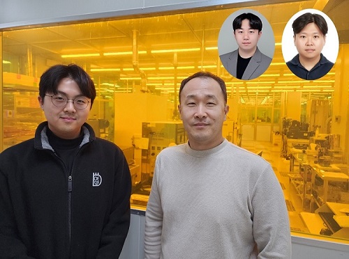
< Photo 1. (from the left) Ph.D. candidate Inki Kim (co-author), Professor SangHyeon Kim (corresponding author), Dr. Joonsup Shim (first author), and Dr. Jinha Lim (co-author) of KAIST School of Electrical Engineering. >
KAIST (represented by President Kwang-Hyung Lee) announced on the 27th of March that a research team led by Professor SangHyeon Kim from the School of Electrical Engineering has developed a mid-infrared photodetector that operates stably at room temperature, marking a major turning point for the commercialization of ultra-compact optical sensors.
The newly developed photodetector utilizes conventional silicon-based CMOS processes, enabling low-cost mass production while maintaining stable operation at room temperature. Notably, the research team successfully demonstrated the real-time detection of carbon dioxide (CO₂) gas using ultra-compact and ultra-thin optical sensors equipped with this photodetector, proving its potential for environmental monitoring and hazardous gas analysis.
Existing mid-infrared photodetectors generally require cooling systems due to high thermal noise at room temperature. These cooling systems increase the size and cost of equipment, making miniaturization and integration into portable devices challenging. Furthermore, conventional mid-infrared photodetectors are incompatible with silicon-based CMOS processes, limiting large-scale production and commercialization.
To address these limitations, the research team developed a waveguide-integrated photodetector using germanium (Ge), a Group IV element like silicon. This approach enables broad-spectrum mid-infrared detection while ensuring stable operation at room temperature.
< Figure 1. Schematic diagram of a room-temperature mid-infrared waveguide-integrated photodetector based on the Ge-on-insulator optical platform proposed in this study (top). Optical microscope image of the integrated photodetector connected with the sensing unit (bottom). >
A waveguide is a structure designed to efficiently guide light along a specific path with minimal loss. To implement various optical functions on a chip (on-chip), the development of waveguide-integrated photodetectors and waveguide-based optical components is essential.
Unlike conventional photodetectors that primarily rely on bandgap absorption principles, this new technology leverages the bolometric effect*, allowing it to detect the entire mid-infrared spectral range. As a result, it can be widely applied to the real-time sensing of various molecular species.
*Bolometric effect: A principle in which light absorption leads to an increase in temperature, causing electrical signals to change accordingly.
The waveguide-integrated mid-infrared photodetector developed by the research team is considered a groundbreaking innovation that overcomes the limitations of existing mid-infrared sensor technologies, including the need for cooling, difficulties in mass production, and high costs.
< Figure 2. Room temperature photoresponse characteristics of the mid-infrared waveguide photodetector proposed in this study (left) and real-time carbon dioxide (CO2) gas sensing results using the photodetector (right). >
This breakthrough technology is expected to be applicable across diverse fields, including environmental monitoring, medical diagnostics, industrial process management, national defense and security, and smart devices. It also paves the way for next-generation mid-infrared sensor advancements.
Professor SangHyeon Kim from KAIST stated, "This research represents a novel approach that overcomes the limitations of existing mid-infrared photodetector technologies and has great potential for practical applications in various fields." He further emphasized, "Since this sensor technology is compatible with CMOS processes, it enables low-cost mass production, making it highly suitable for next-generation environmental monitoring systems and smart manufacturing sites."
< Figure 3. Performance comparison image of a room-temperature mid-infrared waveguide photodetector fabricated with the technology proposed in this study. It achieves the world’s highest performance compared to existing technologies utilizing the Bolometric effect, and is the only solution compatible with CMOS processes. The technology proposed by our research team is characterized by its ability to respond to a wide spectrum of the mid-infrared band without limitations. >
The study, with Dr. Joonsup Shim (currently a postdoctoral researcher at Harvard University) as the first author, was published on March 19, 2025 in the internationally renowned journal Light: Science & Applications (JCR 2.9%, IF=20.6).
(Paper title: “Room-temperature waveguide-integrated photodetector using bolometric effect for mid-infrared spectroscopy applications,” https://doi.org/10.1038/s41377-025-01803-3)
2025.03.27 View 4402
KAIST Innovates Mid-Infrared Photodetectors for Exoplanet Detection, Expanding Applications to Environmental and Medical Fields
NASA’s James Webb Space Telescope (JWST) utilizes mid-infrared spectroscopy to precisely analyze molecular components such as water vapor and sulfur dioxide in exoplanet atmospheres. The key to this analysis, where each molecule exhibits a unique spectral "fingerprint," lies in highly sensitive photodetector technology capable of measuring extremely weak light intensities. Recently, KAIST researchers have developed an innovative photodetector capable of detecting a broad range of mid-infrared spectra, garnering significant attention.
< Photo 1. (from the left) Ph.D. candidate Inki Kim (co-author), Professor SangHyeon Kim (corresponding author), Dr. Joonsup Shim (first author), and Dr. Jinha Lim (co-author) of KAIST School of Electrical Engineering. >
KAIST (represented by President Kwang-Hyung Lee) announced on the 27th of March that a research team led by Professor SangHyeon Kim from the School of Electrical Engineering has developed a mid-infrared photodetector that operates stably at room temperature, marking a major turning point for the commercialization of ultra-compact optical sensors.
The newly developed photodetector utilizes conventional silicon-based CMOS processes, enabling low-cost mass production while maintaining stable operation at room temperature. Notably, the research team successfully demonstrated the real-time detection of carbon dioxide (CO₂) gas using ultra-compact and ultra-thin optical sensors equipped with this photodetector, proving its potential for environmental monitoring and hazardous gas analysis.
Existing mid-infrared photodetectors generally require cooling systems due to high thermal noise at room temperature. These cooling systems increase the size and cost of equipment, making miniaturization and integration into portable devices challenging. Furthermore, conventional mid-infrared photodetectors are incompatible with silicon-based CMOS processes, limiting large-scale production and commercialization.
To address these limitations, the research team developed a waveguide-integrated photodetector using germanium (Ge), a Group IV element like silicon. This approach enables broad-spectrum mid-infrared detection while ensuring stable operation at room temperature.
< Figure 1. Schematic diagram of a room-temperature mid-infrared waveguide-integrated photodetector based on the Ge-on-insulator optical platform proposed in this study (top). Optical microscope image of the integrated photodetector connected with the sensing unit (bottom). >
A waveguide is a structure designed to efficiently guide light along a specific path with minimal loss. To implement various optical functions on a chip (on-chip), the development of waveguide-integrated photodetectors and waveguide-based optical components is essential.
Unlike conventional photodetectors that primarily rely on bandgap absorption principles, this new technology leverages the bolometric effect*, allowing it to detect the entire mid-infrared spectral range. As a result, it can be widely applied to the real-time sensing of various molecular species.
*Bolometric effect: A principle in which light absorption leads to an increase in temperature, causing electrical signals to change accordingly.
The waveguide-integrated mid-infrared photodetector developed by the research team is considered a groundbreaking innovation that overcomes the limitations of existing mid-infrared sensor technologies, including the need for cooling, difficulties in mass production, and high costs.
< Figure 2. Room temperature photoresponse characteristics of the mid-infrared waveguide photodetector proposed in this study (left) and real-time carbon dioxide (CO2) gas sensing results using the photodetector (right). >
This breakthrough technology is expected to be applicable across diverse fields, including environmental monitoring, medical diagnostics, industrial process management, national defense and security, and smart devices. It also paves the way for next-generation mid-infrared sensor advancements.
Professor SangHyeon Kim from KAIST stated, "This research represents a novel approach that overcomes the limitations of existing mid-infrared photodetector technologies and has great potential for practical applications in various fields." He further emphasized, "Since this sensor technology is compatible with CMOS processes, it enables low-cost mass production, making it highly suitable for next-generation environmental monitoring systems and smart manufacturing sites."
< Figure 3. Performance comparison image of a room-temperature mid-infrared waveguide photodetector fabricated with the technology proposed in this study. It achieves the world’s highest performance compared to existing technologies utilizing the Bolometric effect, and is the only solution compatible with CMOS processes. The technology proposed by our research team is characterized by its ability to respond to a wide spectrum of the mid-infrared band without limitations. >
The study, with Dr. Joonsup Shim (currently a postdoctoral researcher at Harvard University) as the first author, was published on March 19, 2025 in the internationally renowned journal Light: Science & Applications (JCR 2.9%, IF=20.6).
(Paper title: “Room-temperature waveguide-integrated photodetector using bolometric effect for mid-infrared spectroscopy applications,” https://doi.org/10.1038/s41377-025-01803-3)
2025.03.27 View 4402 -
 KAIST Secures Core Technology for Ultra-High-Resolution Image Sensors
A joint research team from Korea and the United States has developed next-generation, high-resolution image sensor technology with higher power efficiency and a smaller size compared to existing sensors. Notably, they have secured foundational technology for ultra-high-resolution shortwave infrared (SWIR) image sensors, an area currently dominated by Sony, paving the way for future market entry.
KAIST (represented by President Kwang Hyung Lee) announced on the 20th of November that a research team led by Professor SangHyeon Kim from the School of Electrical Engineering, in collaboration with Inha University and Yale University in the U.S., has developed an ultra-thin broadband photodiode (PD), marking a significant breakthrough in high-performance image sensor technology.
This research drastically improves the trade-off between the absorption layer thickness and quantum efficiency found in conventional photodiode technology. Specifically, it achieved high quantum efficiency of over 70% even in an absorption layer thinner than one micrometer (μm), reducing the thickness of the absorption layer by approximately 70% compared to existing technologies.
A thinner absorption layer simplifies pixel processing, allowing for higher resolution and smoother carrier diffusion, which is advantageous for light carrier acquisition while also reducing the cost. However, a fundamental issue with thinner absorption layers is the reduced absorption of long-wavelength light.
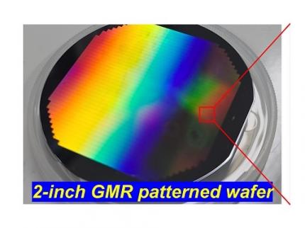
< Figure 1. Schematic diagram of the InGaAs photodiode image sensor integrated on the Guided-Mode Resonance (GMR) structure proposed in this study (left), a photograph of the fabricated wafer, and a scanning electron microscope (SEM) image of the periodic patterns (right) >
The research team introduced a guided-mode resonance (GMR) structure* that enables high-efficiency light absorption across a wide spectral range from 400 nanometers (nm) to 1,700 nanometers (nm). This wavelength range includes not only visible light but also light the SWIR region, making it valuable for various industrial applications.
*Guided-Mode Resonance (GMR) Structure: A concept used in electromagnetics, a phenomenon in which a specific (light) wave resonates (forming a strong electric/magnetic field) at a specific wavelength. Since energy is maximized under these conditions, it has been used to increase antenna or radar efficiency.
The improved performance in the SWIR region is expected to play a significant role in developing next-generation image sensors with increasingly high resolutions. The GMR structure, in particular, holds potential for further enhancing resolution and other performance metrics through hybrid integration and monolithic 3D integration with complementary metal-oxide-semiconductor (CMOS)-based readout integrated circuits (ROIC).
< Figure 2. Benchmark for state-of-the-art InGaAs-based SWIR pixels with simulated EQE lines as a function of TAL variation. Performance is maintained while reducing the absorption layer thickness from 2.1 micrometers or more to 1 micrometer or less while reducing it by 50% to 70% >
The research team has significantly enhanced international competitiveness in low-power devices and ultra-high-resolution imaging technology, opening up possibilities for applications in digital cameras, security systems, medical and industrial image sensors, as well as future ultra-high-resolution sensors for autonomous driving, aerospace, and satellite observation.
Professor Sang Hyun Kim, the lead researcher, commented, “This research demonstrates that significantly higher performance than existing technologies can be achieved even with ultra-thin absorption layers.”
< Figure 3. Top optical microscope image and cross-sectional scanning electron microscope image of the InGaAs photodiode image sensor fabricated on the GMR structure (left). Improved quantum efficiency performance of the ultra-thin image sensor (red) fabricated with the technology proposed in this study (right) >
The results of this research were published on 15th of November, in the prestigious international journal Light: Science & Applications (JCR 2.9%, IF=20.6), with Professor Dae-Myung Geum of Inha University (formerly a KAIST postdoctoral researcher) and Dr. Jinha Lim (currently a postdoctoral researcher at Yale University) as co-first authors. (Paper title: “Highly-efficient (>70%) and Wide-spectral (400 nm -1700 nm) sub-micron-thick InGaAs photodiodes for future high-resolution image sensors”)
This study was supported by the National Research Foundation of Korea.
2024.11.22 View 7398
KAIST Secures Core Technology for Ultra-High-Resolution Image Sensors
A joint research team from Korea and the United States has developed next-generation, high-resolution image sensor technology with higher power efficiency and a smaller size compared to existing sensors. Notably, they have secured foundational technology for ultra-high-resolution shortwave infrared (SWIR) image sensors, an area currently dominated by Sony, paving the way for future market entry.
KAIST (represented by President Kwang Hyung Lee) announced on the 20th of November that a research team led by Professor SangHyeon Kim from the School of Electrical Engineering, in collaboration with Inha University and Yale University in the U.S., has developed an ultra-thin broadband photodiode (PD), marking a significant breakthrough in high-performance image sensor technology.
This research drastically improves the trade-off between the absorption layer thickness and quantum efficiency found in conventional photodiode technology. Specifically, it achieved high quantum efficiency of over 70% even in an absorption layer thinner than one micrometer (μm), reducing the thickness of the absorption layer by approximately 70% compared to existing technologies.
A thinner absorption layer simplifies pixel processing, allowing for higher resolution and smoother carrier diffusion, which is advantageous for light carrier acquisition while also reducing the cost. However, a fundamental issue with thinner absorption layers is the reduced absorption of long-wavelength light.
< Figure 1. Schematic diagram of the InGaAs photodiode image sensor integrated on the Guided-Mode Resonance (GMR) structure proposed in this study (left), a photograph of the fabricated wafer, and a scanning electron microscope (SEM) image of the periodic patterns (right) >
The research team introduced a guided-mode resonance (GMR) structure* that enables high-efficiency light absorption across a wide spectral range from 400 nanometers (nm) to 1,700 nanometers (nm). This wavelength range includes not only visible light but also light the SWIR region, making it valuable for various industrial applications.
*Guided-Mode Resonance (GMR) Structure: A concept used in electromagnetics, a phenomenon in which a specific (light) wave resonates (forming a strong electric/magnetic field) at a specific wavelength. Since energy is maximized under these conditions, it has been used to increase antenna or radar efficiency.
The improved performance in the SWIR region is expected to play a significant role in developing next-generation image sensors with increasingly high resolutions. The GMR structure, in particular, holds potential for further enhancing resolution and other performance metrics through hybrid integration and monolithic 3D integration with complementary metal-oxide-semiconductor (CMOS)-based readout integrated circuits (ROIC).
< Figure 2. Benchmark for state-of-the-art InGaAs-based SWIR pixels with simulated EQE lines as a function of TAL variation. Performance is maintained while reducing the absorption layer thickness from 2.1 micrometers or more to 1 micrometer or less while reducing it by 50% to 70% >
The research team has significantly enhanced international competitiveness in low-power devices and ultra-high-resolution imaging technology, opening up possibilities for applications in digital cameras, security systems, medical and industrial image sensors, as well as future ultra-high-resolution sensors for autonomous driving, aerospace, and satellite observation.
Professor Sang Hyun Kim, the lead researcher, commented, “This research demonstrates that significantly higher performance than existing technologies can be achieved even with ultra-thin absorption layers.”
< Figure 3. Top optical microscope image and cross-sectional scanning electron microscope image of the InGaAs photodiode image sensor fabricated on the GMR structure (left). Improved quantum efficiency performance of the ultra-thin image sensor (red) fabricated with the technology proposed in this study (right) >
The results of this research were published on 15th of November, in the prestigious international journal Light: Science & Applications (JCR 2.9%, IF=20.6), with Professor Dae-Myung Geum of Inha University (formerly a KAIST postdoctoral researcher) and Dr. Jinha Lim (currently a postdoctoral researcher at Yale University) as co-first authors. (Paper title: “Highly-efficient (>70%) and Wide-spectral (400 nm -1700 nm) sub-micron-thick InGaAs photodiodes for future high-resolution image sensors”)
This study was supported by the National Research Foundation of Korea.
2024.11.22 View 7398