EC
-
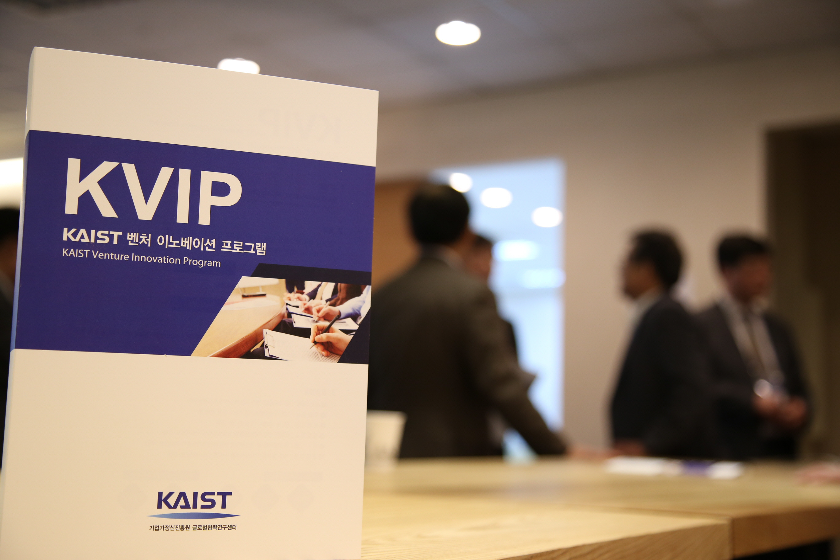 KVIP Opened in Pangyo
KAIST has opened the KAIST Venture Innovation Program (KVIP) in its Center for Industry Outreach, designed for executive and high-ranking officers of venture companies. Located in Pangyo Techno Valley, KAIST’s Center for Industry Outreach was established in collaboration with the government of Gyeonggi Province to support venture companies in Pangyo for business management training, venture networking, and university-industry cooperation.
The program will be held every Monday for 12 weeks from April 13 to July 6 in KAIST’s Center for Industry Outreach. This executive education program mainly focuses on solving problems that arise when a medium-sized venture company is in the course of growing into a global corporation. The program is divided into four courses which will cover business management, competition in the global market, transformation of a company, and technological innovation.
Professors from various departments at KAIST will give lectures on their fields. Professor Jaeseung Jeong from the Bio and Brain Engineering Department, Professor Hoi-Jun Yoo from the Electrical Engineering Department, Professor Sangmin Bae from the Industrial Design Department, and Professor Kwangjae Sung from the Business and Technology Management Department will each deliver lectures on brain engineering, semiconductor, design, and restructuring.
Industry experts are also invited to give talks, including Dr. Dae-Gyu Byun, the Chief Executive Officer and President of HUMAX Electronics, Dr. Gwang-Cheol Choi, the Chief Executive Officer of SK Engineering & Construction, Mr. Il-young Kim, the former Chief Executive Officer of KT, Dr. Jae-hoon Jeong, the President of the Korea Institute for the Advancement of Technology (KIAT), Dr. Intak Bae, the Chief Executive Officer of Summit Partners, and Mr. Kyung-taek Kwak, a film director.
The department has started recruiting first round applicants for the program, targeting executive and high-ranking officers of middle-sized venture companies. The details of the program can be found on its website, kvip.kaist.ac.kr.
2015.03.23 View 11701
KVIP Opened in Pangyo
KAIST has opened the KAIST Venture Innovation Program (KVIP) in its Center for Industry Outreach, designed for executive and high-ranking officers of venture companies. Located in Pangyo Techno Valley, KAIST’s Center for Industry Outreach was established in collaboration with the government of Gyeonggi Province to support venture companies in Pangyo for business management training, venture networking, and university-industry cooperation.
The program will be held every Monday for 12 weeks from April 13 to July 6 in KAIST’s Center for Industry Outreach. This executive education program mainly focuses on solving problems that arise when a medium-sized venture company is in the course of growing into a global corporation. The program is divided into four courses which will cover business management, competition in the global market, transformation of a company, and technological innovation.
Professors from various departments at KAIST will give lectures on their fields. Professor Jaeseung Jeong from the Bio and Brain Engineering Department, Professor Hoi-Jun Yoo from the Electrical Engineering Department, Professor Sangmin Bae from the Industrial Design Department, and Professor Kwangjae Sung from the Business and Technology Management Department will each deliver lectures on brain engineering, semiconductor, design, and restructuring.
Industry experts are also invited to give talks, including Dr. Dae-Gyu Byun, the Chief Executive Officer and President of HUMAX Electronics, Dr. Gwang-Cheol Choi, the Chief Executive Officer of SK Engineering & Construction, Mr. Il-young Kim, the former Chief Executive Officer of KT, Dr. Jae-hoon Jeong, the President of the Korea Institute for the Advancement of Technology (KIAT), Dr. Intak Bae, the Chief Executive Officer of Summit Partners, and Mr. Kyung-taek Kwak, a film director.
The department has started recruiting first round applicants for the program, targeting executive and high-ranking officers of middle-sized venture companies. The details of the program can be found on its website, kvip.kaist.ac.kr.
2015.03.23 View 11701 -
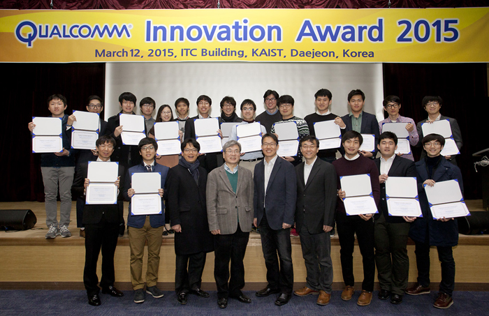 Qualcomm Innovation Award Recognizes 20 KAIST Students
The
award provides research fellowships, worth of USD 100,000, to 20 KAIST graduate
students
With an audience of 100 people present,
KAIST held a ceremony for the Qualcomm Innovation Award 2015 at the Information
Technology Convergence building on campus on March 12, 2015.
The Qualcomm Innovation Award, established
in 2010, is a fellowship that supports innovative science and engineering master’s
and doctoral students at KAIST. Qualcomm donated USD 100,000 to KAIST, stipulating that it be used to foster a creative research environment for graduate
students.
To select the recipients, KAIST formed an award committee chaired
by Professor Soo-Young Lee of the Department of Electrical Engineering and accepted research proposals until late January.
The award committee first selected 37
proposals from 75 papers submitted and then chose the final 20 research
proposals on March 12, 2015 after presentation evaluations. The presentations had to show promise of innovation and creativity; prospective influence on wireless communications
and mobile industry; and the prospect of being implemented.
Each recipient received a USD 4,500 research
fellowship along with an opportunity to present their research findings at a
workshop where Qualcomm engineers and other distinguished individuals of the industry
will attend.
Previously, Qualcomm has donated
research fellowships to KAIST graduate students in 2011 and 2013.
2015.03.19 View 10988
Qualcomm Innovation Award Recognizes 20 KAIST Students
The
award provides research fellowships, worth of USD 100,000, to 20 KAIST graduate
students
With an audience of 100 people present,
KAIST held a ceremony for the Qualcomm Innovation Award 2015 at the Information
Technology Convergence building on campus on March 12, 2015.
The Qualcomm Innovation Award, established
in 2010, is a fellowship that supports innovative science and engineering master’s
and doctoral students at KAIST. Qualcomm donated USD 100,000 to KAIST, stipulating that it be used to foster a creative research environment for graduate
students.
To select the recipients, KAIST formed an award committee chaired
by Professor Soo-Young Lee of the Department of Electrical Engineering and accepted research proposals until late January.
The award committee first selected 37
proposals from 75 papers submitted and then chose the final 20 research
proposals on March 12, 2015 after presentation evaluations. The presentations had to show promise of innovation and creativity; prospective influence on wireless communications
and mobile industry; and the prospect of being implemented.
Each recipient received a USD 4,500 research
fellowship along with an opportunity to present their research findings at a
workshop where Qualcomm engineers and other distinguished individuals of the industry
will attend.
Previously, Qualcomm has donated
research fellowships to KAIST graduate students in 2011 and 2013.
2015.03.19 View 10988 -
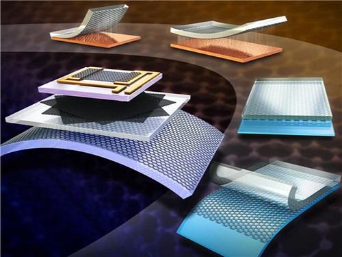
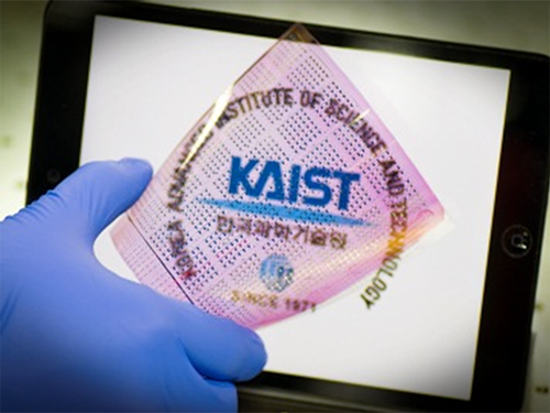 KAIST Develops Ultrathin Polymer Insulators Key to Low-Power Soft Electronics
Using an initiated chemical vapor deposition technique, the research team created an ultrathin polymeric insulating layer essential in realizing transistors with flexibility and low power consumption. This advance is expected to accelerate the commercialization of wearable and soft electronics.
A group of researchers at the Korea Advanced Institute of Science and Technology (KAIST) developed a high-performance ultrathin polymeric insulator for field-effect transistors (FETs). The researchers used vaporized monomers to form polymeric films grown conformally on various surfaces including plastics to produce a versatile insulator that meets a wide range of requirements for next-generation electronic devices. Their research results were published online in Nature Materials on March 9th, 2015.
FETs are an essential component for any modern electronic device used in our daily life from cell phones and computers, to flat-panel displays. Along with three electrodes (gate, source, and drain), FETs consist of an insulating layer and a semiconductor channel layer. The insulator in FETs plays an important role in controlling the conductance of the semiconductor channel and thus current flow within the translators. For reliable and low-power operation of FETs, electrically robust, ultrathin insulators are essential. Conventionally, such insulators are made of inorganic materials (e.g., oxides and nitrides) built on a hard surface such as silicon or glass due to their excellent insulating performance and reliability.
However, these insulators were difficult to implement into soft electronics due to their rigidity and high process temperature. In recent years, many researchers have studied polymers as promising insulating materials that are compatible with soft unconventional substrates and emerging semiconductor materials. The traditional technique employed in developing a polymer insulator, however, had the limitations of low surface coverage at ultra-low thickness, hindering FETs adopting polymeric insulators from operating at low voltage.
A KAIST research team led by Professor Sung Gap Im of the Chemical and Biomolecular Engineering Department and Professor Seunghyup Yoo and Professor Byung Jin Cho of the Electrical Engineering Department developed an insulating layer of organic polymers, “pV3D3,” that can be greatly scaled down, without losing its ideal insulating properties, to a thickness of less than 10 nanometers (nm) using the all-dry vapor-phase technique called the “initiated chemical vapor deposition (iCVD).”
The iCVD process allows gaseous monomers and initiators to react with each other in a low vacuum condition, and as a result, conformal polymeric films with excellent insulating properties are deposited on a substrate. Unlike the traditional technique, the surface-growing character of iCVD can overcome the problems associated with surface tension and produce highly uniform and pure ultrathin polymeric films over a large area with virtually no surface or substrate limitations. Furthermore, most iCVD polymers are created at room temperature, which lessens the strain exerted upon and damage done to the substrates.
With the pV3D3 insulator, the research team built low-power, high-performance FETs based on various semiconductor materials such as organics, graphene, and oxides, demonstrating the pV3D3 insulator’s wide range of material compatibility. They also manufactured a stick-on, removable electronic component using conventional packaging tape as a substrate. In collaboration with Professor Yong-Young Noh from Dongguk University in Korea, the team successfully developed a transistor array on a large-scale flexible substrate with the pV3D3 insulator.
Professor Im said, “The down-scalability and wide range of compatibility observed with iCVD-grown pV3D3 are unprecedented for polymeric insulators. Our iCVD pV3D3 polymeric films showed an insulating performance comparable to that of inorganic insulating layers, even when their thickness were scaled down to sub-10 nm. We expect our development will greatly benefit flexible or soft electronics, which will play a key role in the success of emerging electronic devices such as wearable computers.”
The title of the research paper is “Synthesis of ultrathin polymer insulating layers by initiated chemical vapor deposition for low-power soft electronics” (Digital Object Identifier (DOI) number is 10.1038/nmat4237).
Picture 1: A schematic image to show how the initiated chemical vapor deposition (iCVD) technique produces pV3D3 polymeric films: (i) introduction of vaporized monomers and initiators, (ii) activation of initiators to thermally dissociate into radicals, (iii) adsorption of monomers and initiator radicals onto a substrate, and (iv) transformation of free-radical polymerization into pV3D3 thin films.
Picture 2: This is a transistor array fabricated on a large scale, highly flexible substrate with pV3D3 polymeric films.
Picture 3: This photograph shows an electronic component fabricated on a conventional packaging tape, which is attachable or detachable, with pV3D3 polymeric films embedded.
2015.03.10 View 14257
KAIST Develops Ultrathin Polymer Insulators Key to Low-Power Soft Electronics
Using an initiated chemical vapor deposition technique, the research team created an ultrathin polymeric insulating layer essential in realizing transistors with flexibility and low power consumption. This advance is expected to accelerate the commercialization of wearable and soft electronics.
A group of researchers at the Korea Advanced Institute of Science and Technology (KAIST) developed a high-performance ultrathin polymeric insulator for field-effect transistors (FETs). The researchers used vaporized monomers to form polymeric films grown conformally on various surfaces including plastics to produce a versatile insulator that meets a wide range of requirements for next-generation electronic devices. Their research results were published online in Nature Materials on March 9th, 2015.
FETs are an essential component for any modern electronic device used in our daily life from cell phones and computers, to flat-panel displays. Along with three electrodes (gate, source, and drain), FETs consist of an insulating layer and a semiconductor channel layer. The insulator in FETs plays an important role in controlling the conductance of the semiconductor channel and thus current flow within the translators. For reliable and low-power operation of FETs, electrically robust, ultrathin insulators are essential. Conventionally, such insulators are made of inorganic materials (e.g., oxides and nitrides) built on a hard surface such as silicon or glass due to their excellent insulating performance and reliability.
However, these insulators were difficult to implement into soft electronics due to their rigidity and high process temperature. In recent years, many researchers have studied polymers as promising insulating materials that are compatible with soft unconventional substrates and emerging semiconductor materials. The traditional technique employed in developing a polymer insulator, however, had the limitations of low surface coverage at ultra-low thickness, hindering FETs adopting polymeric insulators from operating at low voltage.
A KAIST research team led by Professor Sung Gap Im of the Chemical and Biomolecular Engineering Department and Professor Seunghyup Yoo and Professor Byung Jin Cho of the Electrical Engineering Department developed an insulating layer of organic polymers, “pV3D3,” that can be greatly scaled down, without losing its ideal insulating properties, to a thickness of less than 10 nanometers (nm) using the all-dry vapor-phase technique called the “initiated chemical vapor deposition (iCVD).”
The iCVD process allows gaseous monomers and initiators to react with each other in a low vacuum condition, and as a result, conformal polymeric films with excellent insulating properties are deposited on a substrate. Unlike the traditional technique, the surface-growing character of iCVD can overcome the problems associated with surface tension and produce highly uniform and pure ultrathin polymeric films over a large area with virtually no surface or substrate limitations. Furthermore, most iCVD polymers are created at room temperature, which lessens the strain exerted upon and damage done to the substrates.
With the pV3D3 insulator, the research team built low-power, high-performance FETs based on various semiconductor materials such as organics, graphene, and oxides, demonstrating the pV3D3 insulator’s wide range of material compatibility. They also manufactured a stick-on, removable electronic component using conventional packaging tape as a substrate. In collaboration with Professor Yong-Young Noh from Dongguk University in Korea, the team successfully developed a transistor array on a large-scale flexible substrate with the pV3D3 insulator.
Professor Im said, “The down-scalability and wide range of compatibility observed with iCVD-grown pV3D3 are unprecedented for polymeric insulators. Our iCVD pV3D3 polymeric films showed an insulating performance comparable to that of inorganic insulating layers, even when their thickness were scaled down to sub-10 nm. We expect our development will greatly benefit flexible or soft electronics, which will play a key role in the success of emerging electronic devices such as wearable computers.”
The title of the research paper is “Synthesis of ultrathin polymer insulating layers by initiated chemical vapor deposition for low-power soft electronics” (Digital Object Identifier (DOI) number is 10.1038/nmat4237).
Picture 1: A schematic image to show how the initiated chemical vapor deposition (iCVD) technique produces pV3D3 polymeric films: (i) introduction of vaporized monomers and initiators, (ii) activation of initiators to thermally dissociate into radicals, (iii) adsorption of monomers and initiator radicals onto a substrate, and (iv) transformation of free-radical polymerization into pV3D3 thin films.
Picture 2: This is a transistor array fabricated on a large scale, highly flexible substrate with pV3D3 polymeric films.
Picture 3: This photograph shows an electronic component fabricated on a conventional packaging tape, which is attachable or detachable, with pV3D3 polymeric films embedded.
2015.03.10 View 14257 -
 Interactions Features KAIST's Human-Computer Interaction Lab
Interactions, a bi-monthly magazine published by the Association for Computing Machinery (ACM), the largest educational and scientific computing society in the world, featured an article introducing Human-Computer Interaction (HCI) Lab at KAIST in the March/April 2015 issue (http://interactions.acm.org/archive/toc/march-april-2015).
Established in 2002, the HCI Lab (http://hcil.kaist.ac.kr/) is run by Professor Geehyuk Lee of the Computer Science Department at KAIST. The lab conducts various research projects to improve the design and operation of physical user interfaces and develops new interaction techniques for new types of computers. For the article, see the link below:
ACM Interactions, March and April 2015
Day in the Lab: Human-Computer Interaction Lab @ KAIST
http://interactions.acm.org/archive/view/march-april-2015/human-computer-interaction-lab-kaist
2015.03.02 View 11331
Interactions Features KAIST's Human-Computer Interaction Lab
Interactions, a bi-monthly magazine published by the Association for Computing Machinery (ACM), the largest educational and scientific computing society in the world, featured an article introducing Human-Computer Interaction (HCI) Lab at KAIST in the March/April 2015 issue (http://interactions.acm.org/archive/toc/march-april-2015).
Established in 2002, the HCI Lab (http://hcil.kaist.ac.kr/) is run by Professor Geehyuk Lee of the Computer Science Department at KAIST. The lab conducts various research projects to improve the design and operation of physical user interfaces and develops new interaction techniques for new types of computers. For the article, see the link below:
ACM Interactions, March and April 2015
Day in the Lab: Human-Computer Interaction Lab @ KAIST
http://interactions.acm.org/archive/view/march-april-2015/human-computer-interaction-lab-kaist
2015.03.02 View 11331 -
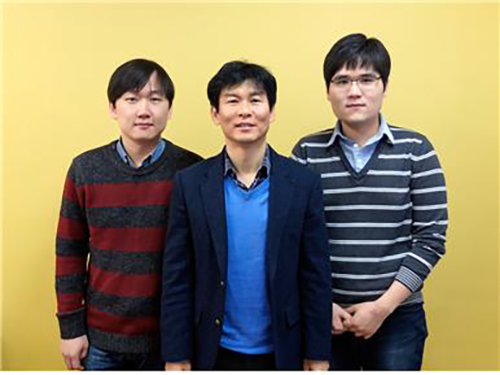 The Real Time Observation of the Birth of a Molecule
From right to left: Dr. Kyung-Hwan Kim, Professor Hyotcherl Lhee, and Jong-Gu Kim, a Ph.D. candidate
Professor Hyotcherl Lhee of the Department of Chemistry at KAIST and Japanese research teams jointly published their research results showing that they have succeeded in the direct observation of how atoms form a molecule in the online issue of Nature on February 19, 2015.
The researchers used water in which gold atoms ([Au(CN) 2- ]) are dissolved and fired X-ray pulses over the specimen in femtosecond timescales to study chemical reactions taking place among the gold atoms. They were able to examine in real time the instant process of how gold atoms bond together to become a molecule, to a trimer or tetramer state.
This direct viewing of the formation of a gold trimer complex ([Au(CN) 2- ] 3 ) will provide an opportunity to understand complex chemical and biological systems.
For details, please see the following press release that was distributed by the High Energy Accelerator Research Organization, KEK, in Japan:
Direct Observation of Bond Formations
February 18, 2015
A collaboration between researchers from KEK, the Institute for Basic Science (IBS), the Korea Advanced Institute of Science and Technology (KAIST), RIKEN, and the Japan Synchrotron Radiation Research Institute (JASRI) used the SACLA X-ray free electron laser (XFEL) facility for a real time visualization of the birth of a molecular that occurs via photoinduced formation of a chemical bonds. This achievement was published in the online version of the scientific journal “Nature” (published on 19 February 2015).
Direct “observation” of the bond making, through a chemical reaction, has been longstanding dream for chemists. However, the distance between atoms is very small, at about 100 picometer, and the bonding is completed very quickly, taking less than one picosecond (ps). Hence, previously, one could only imagine the bond formation between atoms while looking at the chemical reaction progressing in the test-tube.
In this study, the research group focused on the process of photoinduced bond formation between gold (Au) ions dissolved in water. In the ground state (S 0 state in Fig. 1) Au ions that are weakly bound to each other by an electron affinity and aligned in a bent geometry. Upon a photoexcitation, the S 0 state rapidly converts into an excited (S 1 state in Fig. 1) state where Au-Au covalent bonds are formed among Au ions aligned in a linear geometry. Subsequently, the S 1 state transforms to a triplet state (T 1 state in Fig. 1) in 1.6 ps while accompanying further contraction of Au-Au bonds by 0.1 Å. Later, the T 1 state of the trimer converts to a tetramer (tetramer state in Fig. 1) on nanosecond time scale. Finally, the Au ions returned to their original loosely interacting bent structure.
In this research, the direct observation of a very fast chemical reaction, induced by the photo-excitation, was succeeded (Fig. 2, 3). Therefore, this method is expected to be a fundamental technology for understanding the light energy conversion reaction. The research group is actively working to apply this method to the development of viable renewable energy resources, such as a photocatalysts for artificial photosynthesis using sunlight.
This research was supported by the X-ray Free Electron Laser Priority Strategy Program of the MEXT, PRESTO of the JST, and the the Innovative Areas "Artificial Photosynthesis (AnApple)" grant from the Japan Society for the Promotion of Science (JSPS).
Publication: Nature , 518 (19 February 2015)
Title: Direct observation of bond formation in solution with femtosecond X-ray scattering
Authors: K. H. Kim 1 , J. G. Kim 1 , S. Nozawa 1 , T. Sato 1 , K. Y. Oang, T. W. Kim, H. Ki, J. Jo, S. Park, C. Song, T. Sato, K. Ogawa, T. Togashi, K. Tono, M. Yabashi, T. Ishikawa, J. Kim, R. Ryoo, J. Kim, H. Ihee, S. Adachi. ※ 1: These authors contributed equally to the work.
DOI: 10.1038/nature14163
Figure 1. Structure of a gold cyano trimer complex (Au(CN) 2 - ) 3 .
Figure 2. Observed changes in the molecular structure of the gold complex
Figure 3. Schematic view of the research of photo-chemical reactions by the molecular movie
2015.02.27 View 13601
The Real Time Observation of the Birth of a Molecule
From right to left: Dr. Kyung-Hwan Kim, Professor Hyotcherl Lhee, and Jong-Gu Kim, a Ph.D. candidate
Professor Hyotcherl Lhee of the Department of Chemistry at KAIST and Japanese research teams jointly published their research results showing that they have succeeded in the direct observation of how atoms form a molecule in the online issue of Nature on February 19, 2015.
The researchers used water in which gold atoms ([Au(CN) 2- ]) are dissolved and fired X-ray pulses over the specimen in femtosecond timescales to study chemical reactions taking place among the gold atoms. They were able to examine in real time the instant process of how gold atoms bond together to become a molecule, to a trimer or tetramer state.
This direct viewing of the formation of a gold trimer complex ([Au(CN) 2- ] 3 ) will provide an opportunity to understand complex chemical and biological systems.
For details, please see the following press release that was distributed by the High Energy Accelerator Research Organization, KEK, in Japan:
Direct Observation of Bond Formations
February 18, 2015
A collaboration between researchers from KEK, the Institute for Basic Science (IBS), the Korea Advanced Institute of Science and Technology (KAIST), RIKEN, and the Japan Synchrotron Radiation Research Institute (JASRI) used the SACLA X-ray free electron laser (XFEL) facility for a real time visualization of the birth of a molecular that occurs via photoinduced formation of a chemical bonds. This achievement was published in the online version of the scientific journal “Nature” (published on 19 February 2015).
Direct “observation” of the bond making, through a chemical reaction, has been longstanding dream for chemists. However, the distance between atoms is very small, at about 100 picometer, and the bonding is completed very quickly, taking less than one picosecond (ps). Hence, previously, one could only imagine the bond formation between atoms while looking at the chemical reaction progressing in the test-tube.
In this study, the research group focused on the process of photoinduced bond formation between gold (Au) ions dissolved in water. In the ground state (S 0 state in Fig. 1) Au ions that are weakly bound to each other by an electron affinity and aligned in a bent geometry. Upon a photoexcitation, the S 0 state rapidly converts into an excited (S 1 state in Fig. 1) state where Au-Au covalent bonds are formed among Au ions aligned in a linear geometry. Subsequently, the S 1 state transforms to a triplet state (T 1 state in Fig. 1) in 1.6 ps while accompanying further contraction of Au-Au bonds by 0.1 Å. Later, the T 1 state of the trimer converts to a tetramer (tetramer state in Fig. 1) on nanosecond time scale. Finally, the Au ions returned to their original loosely interacting bent structure.
In this research, the direct observation of a very fast chemical reaction, induced by the photo-excitation, was succeeded (Fig. 2, 3). Therefore, this method is expected to be a fundamental technology for understanding the light energy conversion reaction. The research group is actively working to apply this method to the development of viable renewable energy resources, such as a photocatalysts for artificial photosynthesis using sunlight.
This research was supported by the X-ray Free Electron Laser Priority Strategy Program of the MEXT, PRESTO of the JST, and the the Innovative Areas "Artificial Photosynthesis (AnApple)" grant from the Japan Society for the Promotion of Science (JSPS).
Publication: Nature , 518 (19 February 2015)
Title: Direct observation of bond formation in solution with femtosecond X-ray scattering
Authors: K. H. Kim 1 , J. G. Kim 1 , S. Nozawa 1 , T. Sato 1 , K. Y. Oang, T. W. Kim, H. Ki, J. Jo, S. Park, C. Song, T. Sato, K. Ogawa, T. Togashi, K. Tono, M. Yabashi, T. Ishikawa, J. Kim, R. Ryoo, J. Kim, H. Ihee, S. Adachi. ※ 1: These authors contributed equally to the work.
DOI: 10.1038/nature14163
Figure 1. Structure of a gold cyano trimer complex (Au(CN) 2 - ) 3 .
Figure 2. Observed changes in the molecular structure of the gold complex
Figure 3. Schematic view of the research of photo-chemical reactions by the molecular movie
2015.02.27 View 13601 -
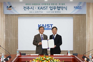 KAIST Signs MOU with Jeonju City
KAIST signed a memorandum of understanding for the development of new industries based on convergence technology with the government of Jeonju City on February 26, 2015. Located in the south west portion of the Korean peninsula, Jeonju City is home to a rich historical and cultural heritage.
Taking advantage of its proximity to the university's campus, the city will cooperate with KAIST to develop the local economy through creating new industries and jobs. To that end, KAIST and Jeonju will foster carbon-based industry, 3D printing technology, the Internet of Things, and emerging technologies. The two organizations also hope this cooperation will produce highly educated manpower for research and development in the city and offer the city to conduct national research projects.
President Sung-Mo Kang and Mayor Seung-Soo Kim pose after signing in the picture below.
2015.02.26 View 8451
KAIST Signs MOU with Jeonju City
KAIST signed a memorandum of understanding for the development of new industries based on convergence technology with the government of Jeonju City on February 26, 2015. Located in the south west portion of the Korean peninsula, Jeonju City is home to a rich historical and cultural heritage.
Taking advantage of its proximity to the university's campus, the city will cooperate with KAIST to develop the local economy through creating new industries and jobs. To that end, KAIST and Jeonju will foster carbon-based industry, 3D printing technology, the Internet of Things, and emerging technologies. The two organizations also hope this cooperation will produce highly educated manpower for research and development in the city and offer the city to conduct national research projects.
President Sung-Mo Kang and Mayor Seung-Soo Kim pose after signing in the picture below.
2015.02.26 View 8451 -
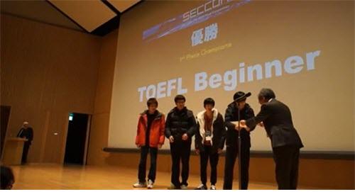 KAIST Team Wins International Hacking Competition, "SECCON CTF 2014"
KAIST’s white hacker team, “TOFEL Beginner,” secured the first place in an international hacking competition, SECCON CTF 2014. SECCON is an international hacking competition which has operated for more than 20 years. It uses the Capture the Flag (CTF) method. Last year’s competition was held in Tokyo on December 7, 2014.
The TOFEL Beginner team consisted of two KAIST graduate students and two researchers from a private security company based in Korea: In-Soo Yoon of Computer Science, Eun-Soo Kim of the Graduate School of Information Security (GSIS), and Jong-Ho Lee and Jung-Hoon Lee of Raon Secure.
Of 4,186 competitors, 24 teams made it to the finals. The TOFEL Beginner took the lead with 4,506 points compared with HITCON (3,112 points) of Taiwan and PPP (2,858 points) of the USA.
With this victory, the KAIST team qualified to participate in the most renowned international hacking competition, the DEF CON Hacking Conference in 2015.
Professor Yongdae Kim of the Electrical Engineering Department at KAIST, who advised the TOEFL Beginner team, said, “Our members have achieved an outstanding result. By taking advantage of this opportunity, KAIST will continue to offer the best programs in information security in Korea and hopefully beyond.”
2015.02.24 View 10959
KAIST Team Wins International Hacking Competition, "SECCON CTF 2014"
KAIST’s white hacker team, “TOFEL Beginner,” secured the first place in an international hacking competition, SECCON CTF 2014. SECCON is an international hacking competition which has operated for more than 20 years. It uses the Capture the Flag (CTF) method. Last year’s competition was held in Tokyo on December 7, 2014.
The TOFEL Beginner team consisted of two KAIST graduate students and two researchers from a private security company based in Korea: In-Soo Yoon of Computer Science, Eun-Soo Kim of the Graduate School of Information Security (GSIS), and Jong-Ho Lee and Jung-Hoon Lee of Raon Secure.
Of 4,186 competitors, 24 teams made it to the finals. The TOFEL Beginner took the lead with 4,506 points compared with HITCON (3,112 points) of Taiwan and PPP (2,858 points) of the USA.
With this victory, the KAIST team qualified to participate in the most renowned international hacking competition, the DEF CON Hacking Conference in 2015.
Professor Yongdae Kim of the Electrical Engineering Department at KAIST, who advised the TOEFL Beginner team, said, “Our members have achieved an outstanding result. By taking advantage of this opportunity, KAIST will continue to offer the best programs in information security in Korea and hopefully beyond.”
2015.02.24 View 10959 -
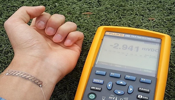 KAIST's Thermoelectric Generator on Glass Fabric Receives the Grand Prize at the Netexplo Forum 2015
The forum announced top ten IT innovations expected to change the world and selected the grand prize on February 4, 2014.
Established in 2007 by Martine Bidegain and Thierry Happe in partnership with the French Senate and the French Ministry for the Digital Economy, the Netexplo Observatory is an independent global organization that studies the impact of digital technology and innovation on society and business.
Every year, the Netexplo Observatory hosts an international conference, the Netexplo Forum, in Paris, France, which surveys digital innovation worldwide. The 8th forum was held in partnership with the United Nations Educational, Scientific and Cultural Organization (UNESCO) on February 4-5, 2015, at the UNESCO House in Paris.
Prior to the conference, the Netexplo Forum 2015 named the top ten most promising digital technologies that will greatly impact the world.
Among them was Professor Byung Jin Cho’s research on a wearable thermoelectric generator (http://www.eurekalert.org/pub_releases/2014-04/tkai-tgo041014.php). The generator was selected as the most innovative technology this year.
Professor Cho of KAIST’s Electrical Engineering Department developed a glass fabric-based thermoelectric generator that is extremely light and flexible and that produces electricity from the heat of the human body. This technology can be applied widely to wearable computers and mobile devices.
The full list of innovations follows below:
Wearable Thermo-Element, South Korea: The human body becomes a source of energy for mobile devices.
W.Afate 3D-printer, Togo: An environmentally friendly fablab that makes a low-cost 3D-printer from recycling electronic components.
Slack, USA: By combining email, Skype, and file-sharing and social networks, internal communication becomes much easier and simpler.
PhotoMath, Croatia: A free app that enables smartphone users to solve mathematical problems simply by scanning the mathematical texts.
Kappo, Chile: Connected cyclists produce and transmit useful data for urban planning to make the city more bike-friendly.
Branching Minds, USA: An improved learning process for students in difficulty through a personalized approach.
Baidu Kuai Sou, China: Smart chopsticks that can check food hazards.
SCio, Israel: A pocket molecular sensor with various applications and data
Rainforest Connection, USA: Fighting deforestation with recycled smartphones
Sense Ebola Followup, Nigeria: A mobile tool to help contain Ebola
For more details on the wearable thermos-element which received the 2015 Netexplo Award, please go to https://www.netexplo.org/en/intelligence/innovation/wearable-thermo-element.
Pictures 1 and 2: A high-performance wearable thermoelectric generator that is extremely flexible and light.
Picture 3: Senator Catherine Morin-Desailly (left) of the French Parliament presents the 2015 Netexplo Award to Professor Byung Jin Cho (right) on February 4, 2015 at the UNESCO House in Paris.
Credit of Loran Dhérines
Picture 4: Professor Byung Jin Cho (left) poses with Dr. Joël de Rosnay (right).
Credit of Loran Dhérines
2015.02.06 View 15535
KAIST's Thermoelectric Generator on Glass Fabric Receives the Grand Prize at the Netexplo Forum 2015
The forum announced top ten IT innovations expected to change the world and selected the grand prize on February 4, 2014.
Established in 2007 by Martine Bidegain and Thierry Happe in partnership with the French Senate and the French Ministry for the Digital Economy, the Netexplo Observatory is an independent global organization that studies the impact of digital technology and innovation on society and business.
Every year, the Netexplo Observatory hosts an international conference, the Netexplo Forum, in Paris, France, which surveys digital innovation worldwide. The 8th forum was held in partnership with the United Nations Educational, Scientific and Cultural Organization (UNESCO) on February 4-5, 2015, at the UNESCO House in Paris.
Prior to the conference, the Netexplo Forum 2015 named the top ten most promising digital technologies that will greatly impact the world.
Among them was Professor Byung Jin Cho’s research on a wearable thermoelectric generator (http://www.eurekalert.org/pub_releases/2014-04/tkai-tgo041014.php). The generator was selected as the most innovative technology this year.
Professor Cho of KAIST’s Electrical Engineering Department developed a glass fabric-based thermoelectric generator that is extremely light and flexible and that produces electricity from the heat of the human body. This technology can be applied widely to wearable computers and mobile devices.
The full list of innovations follows below:
Wearable Thermo-Element, South Korea: The human body becomes a source of energy for mobile devices.
W.Afate 3D-printer, Togo: An environmentally friendly fablab that makes a low-cost 3D-printer from recycling electronic components.
Slack, USA: By combining email, Skype, and file-sharing and social networks, internal communication becomes much easier and simpler.
PhotoMath, Croatia: A free app that enables smartphone users to solve mathematical problems simply by scanning the mathematical texts.
Kappo, Chile: Connected cyclists produce and transmit useful data for urban planning to make the city more bike-friendly.
Branching Minds, USA: An improved learning process for students in difficulty through a personalized approach.
Baidu Kuai Sou, China: Smart chopsticks that can check food hazards.
SCio, Israel: A pocket molecular sensor with various applications and data
Rainforest Connection, USA: Fighting deforestation with recycled smartphones
Sense Ebola Followup, Nigeria: A mobile tool to help contain Ebola
For more details on the wearable thermos-element which received the 2015 Netexplo Award, please go to https://www.netexplo.org/en/intelligence/innovation/wearable-thermo-element.
Pictures 1 and 2: A high-performance wearable thermoelectric generator that is extremely flexible and light.
Picture 3: Senator Catherine Morin-Desailly (left) of the French Parliament presents the 2015 Netexplo Award to Professor Byung Jin Cho (right) on February 4, 2015 at the UNESCO House in Paris.
Credit of Loran Dhérines
Picture 4: Professor Byung Jin Cho (left) poses with Dr. Joël de Rosnay (right).
Credit of Loran Dhérines
2015.02.06 View 15535 -
 News Article: Flexible, High-performance Nonvolatile Memory Developed with SONOS Technology
Professor Yang-Kyu Choi of KAIST’s Department of Electrical Engineering and his team presented a research paper entitled “Flexible High-performance Nonvolatile Memory by Transferring GAA Silicon Nanowire SONOS onto a Plastic Substrate” at the conference of the International Electron Devices Meeting that took place on December 15-17, 2014 in San Francisco.
The Electronic Engineering Journal (http://www.eejournal.com/) recently posted an article on the paper:
Electronic Engineering Journal, February 2, 2015
“A Flat-Earth Memory”
Another Way to Make the Brittle Flexible
http://www.techfocusmedia.net/archives/articles/20150202-flexiblegaa/?printView=true
2015.02.03 View 8320
News Article: Flexible, High-performance Nonvolatile Memory Developed with SONOS Technology
Professor Yang-Kyu Choi of KAIST’s Department of Electrical Engineering and his team presented a research paper entitled “Flexible High-performance Nonvolatile Memory by Transferring GAA Silicon Nanowire SONOS onto a Plastic Substrate” at the conference of the International Electron Devices Meeting that took place on December 15-17, 2014 in San Francisco.
The Electronic Engineering Journal (http://www.eejournal.com/) recently posted an article on the paper:
Electronic Engineering Journal, February 2, 2015
“A Flat-Earth Memory”
Another Way to Make the Brittle Flexible
http://www.techfocusmedia.net/archives/articles/20150202-flexiblegaa/?printView=true
2015.02.03 View 8320 -
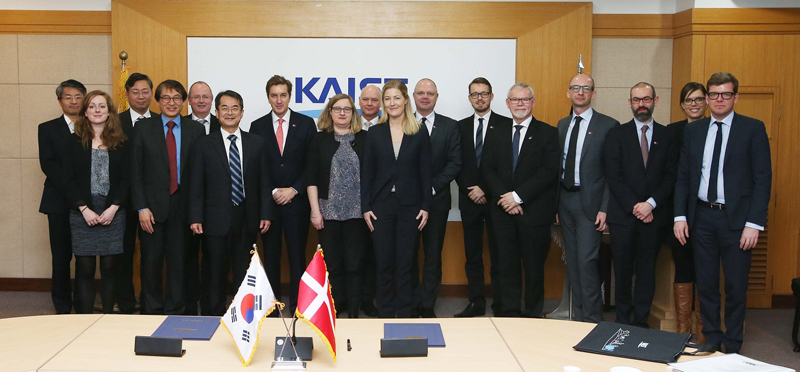 Danish Minister for Higher Education and Science Visits KAIST
Sofie Carsten Nielsen, the Minister for Higher Education and Science of Denmark, accompanied by her delegation, visited KAIST on January 21, 2015 to study outstanding cases of creative economy and to discuss methods of cooperation.
Her delegation included other distinguished members including Thomas Lehmann, the Danish ambassador to Korea, Peter Olesen, Chairman of Innovation Foundation Denmark Governing Board, and Martin Bendsøe, Senior Vice President and Dean of Technical University of Denmark.
After attending the "Electronic Communication Double Degree Agreement" signing ceremony between KAIST’s Department of Electrical Engineering and the Technical University of Denmark, Minister Nielsen visited KAIST’s Institute of Entrepreneurship to observe bilateral industry-university collaborations between KAIST and Denmark and discussed future development plans.
Also, the Grundfos Student Innovation Camp, sponsored by Grundfos, the world's largest pump manufacturer based in Denmark, took place at KAIST from October 26-31, 2014 where Grundfos professionals as well as students from Seoul National University, KAIST, and Technical University of Denmark (DTU) exchanged ideas and opinions on energy efficiency.
KAIST is currently conducting 19 collaborative projects including seven joint researches and seven joint degrees with DTU.
Minister Sofie Carsten Nielsen stands fifth from the left in the front row in the first picture below.
2015.01.27 View 10402
Danish Minister for Higher Education and Science Visits KAIST
Sofie Carsten Nielsen, the Minister for Higher Education and Science of Denmark, accompanied by her delegation, visited KAIST on January 21, 2015 to study outstanding cases of creative economy and to discuss methods of cooperation.
Her delegation included other distinguished members including Thomas Lehmann, the Danish ambassador to Korea, Peter Olesen, Chairman of Innovation Foundation Denmark Governing Board, and Martin Bendsøe, Senior Vice President and Dean of Technical University of Denmark.
After attending the "Electronic Communication Double Degree Agreement" signing ceremony between KAIST’s Department of Electrical Engineering and the Technical University of Denmark, Minister Nielsen visited KAIST’s Institute of Entrepreneurship to observe bilateral industry-university collaborations between KAIST and Denmark and discussed future development plans.
Also, the Grundfos Student Innovation Camp, sponsored by Grundfos, the world's largest pump manufacturer based in Denmark, took place at KAIST from October 26-31, 2014 where Grundfos professionals as well as students from Seoul National University, KAIST, and Technical University of Denmark (DTU) exchanged ideas and opinions on energy efficiency.
KAIST is currently conducting 19 collaborative projects including seven joint researches and seven joint degrees with DTU.
Minister Sofie Carsten Nielsen stands fifth from the left in the front row in the first picture below.
2015.01.27 View 10402 -
 KAIST Develops a Method to Transfer Graphene by Stamping
Professor Sung-Yool Choi’s research team from KAIST's Department of Electrical Engineering has developed a technique that can produce a single-layer graphene from a metal etching. Through this, transferring a graphene layer onto a circuit board can be done as easily as stamping a seal on paper.
The research findings were published in the January 14th issue of Small as the lead article.
This technology will allow different types of wafer transfer methods such as transfer onto a surface of a device or a curved surface, and large surface transfer onto a 4 inch wafer. It will be applied in the field of wearable smart gadgets through commercialization of graphene electronic devices.
The traditional method used to transfer graphene onto a circuit board is a wet transfer. However, it has some drawbacks as the graphene layer can be damaged or contaminated during the transfer process from residue from the metal etching. This may affect the electrical properties of the transferred graphene.
After a graphene growth substrate formed on a catalytic metal substrate is pretreated in an aqueous poly vinyl alcohol (PVA) solution, a PVA film forms on the pretreated substrate. The substrate and the graphene layers bond strongly. The graphene is lifted from the growth substrate by means of an elastomeric stamp.
The delaminated graphene layer is isolated state from the elastomeric stamp and thus can be freely transferred onto a circuit board. As the catalytic metal substrate can be reused and does not contain harmful chemical substances, such transfer method is very eco-friendly.
Professor Choi said, “As the new graphene transfer method has a wide range of applications and allows a large surface transfer, it will contribute to the commercialization of graphene electronic devices.” He added that “because this technique has a high degree of freedom in transfer process, it has a variety of usages for graphene and 2 dimensional nano-devices.”
This research was sponsored by the Ministry of Science, ICT and Future Planning, the Republic of Korea.
Figure 1. Cover photo of the journal Small which illustrates the research findings
Figure 2. Above view of Graphene layer transferred through the new method
Figure 3. Large surface transfer of Graphene
2015.01.23 View 12164
KAIST Develops a Method to Transfer Graphene by Stamping
Professor Sung-Yool Choi’s research team from KAIST's Department of Electrical Engineering has developed a technique that can produce a single-layer graphene from a metal etching. Through this, transferring a graphene layer onto a circuit board can be done as easily as stamping a seal on paper.
The research findings were published in the January 14th issue of Small as the lead article.
This technology will allow different types of wafer transfer methods such as transfer onto a surface of a device or a curved surface, and large surface transfer onto a 4 inch wafer. It will be applied in the field of wearable smart gadgets through commercialization of graphene electronic devices.
The traditional method used to transfer graphene onto a circuit board is a wet transfer. However, it has some drawbacks as the graphene layer can be damaged or contaminated during the transfer process from residue from the metal etching. This may affect the electrical properties of the transferred graphene.
After a graphene growth substrate formed on a catalytic metal substrate is pretreated in an aqueous poly vinyl alcohol (PVA) solution, a PVA film forms on the pretreated substrate. The substrate and the graphene layers bond strongly. The graphene is lifted from the growth substrate by means of an elastomeric stamp.
The delaminated graphene layer is isolated state from the elastomeric stamp and thus can be freely transferred onto a circuit board. As the catalytic metal substrate can be reused and does not contain harmful chemical substances, such transfer method is very eco-friendly.
Professor Choi said, “As the new graphene transfer method has a wide range of applications and allows a large surface transfer, it will contribute to the commercialization of graphene electronic devices.” He added that “because this technique has a high degree of freedom in transfer process, it has a variety of usages for graphene and 2 dimensional nano-devices.”
This research was sponsored by the Ministry of Science, ICT and Future Planning, the Republic of Korea.
Figure 1. Cover photo of the journal Small which illustrates the research findings
Figure 2. Above view of Graphene layer transferred through the new method
Figure 3. Large surface transfer of Graphene
2015.01.23 View 12164 -
 President Kang to Present at the World Economic Forum
President Sung-Mo Kang of KAIST will attend the World Economic Forum (WEF) as a member of the Global University Leaders Forum (GULF) to represent KAIST. GULF is attended by the world leaders of education and research. Its members represent 26 universities drawn from around the world including Harvard University. KAIST is the only Korean university to be invited.
WEF will be held in Davos, Switzerland, for four days, starting on 21 January 2015. He will discuss the future of higher education, the issues and solutions of science and society at GULF.
By attending GULF, KAIST expects to strengthen its network with top universities around the world and raise KAIST’s profile on an international basis. President Kang said, “The invitation for KAIST to attend the GULF is an evidence of its raised global status.” He continued, “I will show the innovative and challenging achievements KAIST has made to the leaders of the world.”
The theme of the 2015 World Economic Forum Annual Meeting 2015 is “The New Global Context” to discuss the integration of economic growth and society, employment and work force, environment and resource scarcity, the future of the Internet, and international crime and anti-corruption.
The World Economic Forum was established in 1971 by Klaus Schwab who is also its Executive Chairman. More than 2,500 people including German Chancellor Angela Merkel, French President François Hollande, Chinese Premier Li Keqiang, Google President Eric Schmidt, and Microsoft CEO Satya Nadella will attend this year's forum.
2015.01.22 View 9408
President Kang to Present at the World Economic Forum
President Sung-Mo Kang of KAIST will attend the World Economic Forum (WEF) as a member of the Global University Leaders Forum (GULF) to represent KAIST. GULF is attended by the world leaders of education and research. Its members represent 26 universities drawn from around the world including Harvard University. KAIST is the only Korean university to be invited.
WEF will be held in Davos, Switzerland, for four days, starting on 21 January 2015. He will discuss the future of higher education, the issues and solutions of science and society at GULF.
By attending GULF, KAIST expects to strengthen its network with top universities around the world and raise KAIST’s profile on an international basis. President Kang said, “The invitation for KAIST to attend the GULF is an evidence of its raised global status.” He continued, “I will show the innovative and challenging achievements KAIST has made to the leaders of the world.”
The theme of the 2015 World Economic Forum Annual Meeting 2015 is “The New Global Context” to discuss the integration of economic growth and society, employment and work force, environment and resource scarcity, the future of the Internet, and international crime and anti-corruption.
The World Economic Forum was established in 1971 by Klaus Schwab who is also its Executive Chairman. More than 2,500 people including German Chancellor Angela Merkel, French President François Hollande, Chinese Premier Li Keqiang, Google President Eric Schmidt, and Microsoft CEO Satya Nadella will attend this year's forum.
2015.01.22 View 9408