Chem
-
 Printed Thermo-Plasmonic Heat Patterns for Neurological Disorder Treatment
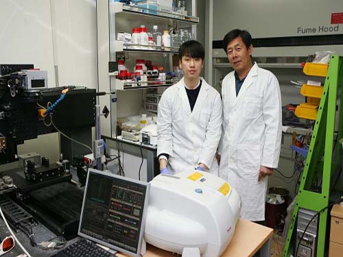
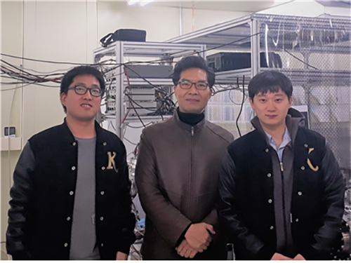
(Professor Nam and Dr. Kang, right)
A KAIST team presented a highly customizable neural stimulation method. The research team developed a technology that can print the heat pattern on a micron scale to enable the control of biological activities remotely.
The researchers integrated a precision inkjet printing technology with bio-functional thermo-plasmonic nanoparticles to achieve a ‘selective nano-photothermal neural stimulation method.’
The research team of Professor Yoonkey Nam at the Department of Bio and Brain Engineering expects this will serve as an enabling technology for personalized precision neuromodulation therapy for patients with neurological disorders.
The nano-photothermal neural stimulation method uses the thermo-plasmonic effect of metal nanoparticles to modulate the activities of neuronal networks. With the thermo-plasmonic effect, metal nanoparticles can absorb specific wavelength of illuminated light to efficiently generate localized heat. The research team discovered the inhibitory behavior of spontaneous activities of neurons upon photothermal stimulation four years ago. Since then, they have developed this technology to control hyperactive behaviors of neurons and neural circuits, which is often found in neurological disorders such as epilepsy.
In order to overcome the limitation on the spatial selectivity and resolution of the previously developed nano-photothermal method, the team adopted an inkjet printing technology to micro pattern the plasmonic nanoparticles (a few tens of microns), and successfully demonstrated that the nano-photothermal stimulation can be selectively applied according to the printed patterns.
The researchers applied a polyelectrolyte layer-by-layer coating method to printing substrates in a way to improve the pattern fidelity and achieve the uniform assembly of nanoparticles. The electrostatic attraction between the printed nanoparticles and the coated printing substrate also helped the stability of the attached nanoparticles. Because the polyelectrolyte coating is biocompatible, biological experiments including cell culture are possible with the technology developed in this work.
Using printed gold nanorod particles in a few tens of microns resolution over a several centimeters area, the researchers showed that highly complex heat patterns can be precisely formed upon light illumination according to the printing image.
Lastly, the team confirmed that the printed heat patterns can selectively and instantaneously inhibit the activities of cultured hippocampal neurons upon near-infrared light illumination. Because the printing process is applicable to thin and flexible substrates, the technology can be easily applied to implantable neurological disorder treatment devices and wearable devices. By selectively applying the heat patterns to only the desired cellular areas, customized and personalized photothermal neuromodulation therapy can be applied to patients.
“The fact that any desired heat patterns can be simply ‘printed’ anywhere broadens the applicability of this technology in many engineering fields. In bioengineering, it can be applied to neural interfaces using light and heat to modulate physiological functions. As another engineering application, for example, printed heat patterns can be used as a new concept of anti-counterfeit applications,” said the principal investigator, Yoonkey Nam at KAIST. This work, led mainly by Dr. Hongki Kang, was published in ACS Nano on February 5th 2018.
2018.04.06 View 7860
Printed Thermo-Plasmonic Heat Patterns for Neurological Disorder Treatment
(Professor Nam and Dr. Kang, right)
A KAIST team presented a highly customizable neural stimulation method. The research team developed a technology that can print the heat pattern on a micron scale to enable the control of biological activities remotely.
The researchers integrated a precision inkjet printing technology with bio-functional thermo-plasmonic nanoparticles to achieve a ‘selective nano-photothermal neural stimulation method.’
The research team of Professor Yoonkey Nam at the Department of Bio and Brain Engineering expects this will serve as an enabling technology for personalized precision neuromodulation therapy for patients with neurological disorders.
The nano-photothermal neural stimulation method uses the thermo-plasmonic effect of metal nanoparticles to modulate the activities of neuronal networks. With the thermo-plasmonic effect, metal nanoparticles can absorb specific wavelength of illuminated light to efficiently generate localized heat. The research team discovered the inhibitory behavior of spontaneous activities of neurons upon photothermal stimulation four years ago. Since then, they have developed this technology to control hyperactive behaviors of neurons and neural circuits, which is often found in neurological disorders such as epilepsy.
In order to overcome the limitation on the spatial selectivity and resolution of the previously developed nano-photothermal method, the team adopted an inkjet printing technology to micro pattern the plasmonic nanoparticles (a few tens of microns), and successfully demonstrated that the nano-photothermal stimulation can be selectively applied according to the printed patterns.
The researchers applied a polyelectrolyte layer-by-layer coating method to printing substrates in a way to improve the pattern fidelity and achieve the uniform assembly of nanoparticles. The electrostatic attraction between the printed nanoparticles and the coated printing substrate also helped the stability of the attached nanoparticles. Because the polyelectrolyte coating is biocompatible, biological experiments including cell culture are possible with the technology developed in this work.
Using printed gold nanorod particles in a few tens of microns resolution over a several centimeters area, the researchers showed that highly complex heat patterns can be precisely formed upon light illumination according to the printing image.
Lastly, the team confirmed that the printed heat patterns can selectively and instantaneously inhibit the activities of cultured hippocampal neurons upon near-infrared light illumination. Because the printing process is applicable to thin and flexible substrates, the technology can be easily applied to implantable neurological disorder treatment devices and wearable devices. By selectively applying the heat patterns to only the desired cellular areas, customized and personalized photothermal neuromodulation therapy can be applied to patients.
“The fact that any desired heat patterns can be simply ‘printed’ anywhere broadens the applicability of this technology in many engineering fields. In bioengineering, it can be applied to neural interfaces using light and heat to modulate physiological functions. As another engineering application, for example, printed heat patterns can be used as a new concept of anti-counterfeit applications,” said the principal investigator, Yoonkey Nam at KAIST. This work, led mainly by Dr. Hongki Kang, was published in ACS Nano on February 5th 2018.
2018.04.06 View 7860 -
 Developing Flexible Vertical Micro LED
A KAIST research team led by Professor Keon Jae Lee from the Department of Materials Science and Engineering and Professor Daesoo Kim from the Department of Biological Sciences has developed flexible vertical micro LEDs (f-VLEDs) using anisotropic conductive film (ACF)-based transfer and interconnection technology. The team also succeeded in controlling animal behavior via optogenetic stimulation of the f-VLEDs.
Flexible micro LEDs have become a strong candidate for the next-generation display due to their ultra-low power consumption, fast response speed, and excellent flexibility. However, the previous micro LED technology had critical issues such as poor device efficiency, low thermal reliability, and the lack of interconnection technology for high-resolution micro LED displays.
The research team has designed new transfer equipment and fabricated a f-VLED array (50ⅹ50) using simultaneous transfer and interconnection through the precise alignment of ACF bonding process. These f-VLEDs (thickness: 5 ㎛, size: below 80 ㎛) achieved optical power density (30 mW/mm2) three times higher than that of lateral micro LEDs, improving thermal reliability and lifetime by reducing heat generation within the thin film LEDs.
These f-VLEDs can be applied to optogenetics for controlling the behavior of neuron cells and brains. In contrast to the electrical stimulation that activates all of the neurons in brain, optogenetics can stimulate specific excitatory or inhibitory neurons within the localized cortical areas of the brain, which facilitates precise analysis, high-resolution mapping, and neuron modulation of animal brains. (Refer to the author’s previous ACS Nano paper of “Optogenetic Mapping of Functional Connectivity in Freely Moving Mice via Insertable Wrapping Electrode Array Beneath the Skull.” )
In this work, they inserted the innovative f-VLEDs into the narrow space between the skull and the brain surface and succeeded in controlling mouse behavior by illuminating motor neurons on two-dimensional cortical areas located deep below the brain surface.
Professor Lee said, “The flexible vertical micro LED can be used in low-power smart watches, mobile displays, and wearable lighting. In addition, these flexible optoelectronic devices are suitable for biomedical applications such as brain science, phototherapeutic treatment, and contact lens biosensors.”
He recently established a startup company ( FRONICS Inc. ) based on micro LED technology and is looking for global partnerships for commercialization. This result entitled “ Optogenetic Control of Body Movements via Flexible Vertical Light-Emitting Diodes on Brain Surface ” was published in the February 2018 issue of Nano Energy.
Figure 1. Comparison of μ-LEDs Technology
2018.01.29 View 15008
Developing Flexible Vertical Micro LED
A KAIST research team led by Professor Keon Jae Lee from the Department of Materials Science and Engineering and Professor Daesoo Kim from the Department of Biological Sciences has developed flexible vertical micro LEDs (f-VLEDs) using anisotropic conductive film (ACF)-based transfer and interconnection technology. The team also succeeded in controlling animal behavior via optogenetic stimulation of the f-VLEDs.
Flexible micro LEDs have become a strong candidate for the next-generation display due to their ultra-low power consumption, fast response speed, and excellent flexibility. However, the previous micro LED technology had critical issues such as poor device efficiency, low thermal reliability, and the lack of interconnection technology for high-resolution micro LED displays.
The research team has designed new transfer equipment and fabricated a f-VLED array (50ⅹ50) using simultaneous transfer and interconnection through the precise alignment of ACF bonding process. These f-VLEDs (thickness: 5 ㎛, size: below 80 ㎛) achieved optical power density (30 mW/mm2) three times higher than that of lateral micro LEDs, improving thermal reliability and lifetime by reducing heat generation within the thin film LEDs.
These f-VLEDs can be applied to optogenetics for controlling the behavior of neuron cells and brains. In contrast to the electrical stimulation that activates all of the neurons in brain, optogenetics can stimulate specific excitatory or inhibitory neurons within the localized cortical areas of the brain, which facilitates precise analysis, high-resolution mapping, and neuron modulation of animal brains. (Refer to the author’s previous ACS Nano paper of “Optogenetic Mapping of Functional Connectivity in Freely Moving Mice via Insertable Wrapping Electrode Array Beneath the Skull.” )
In this work, they inserted the innovative f-VLEDs into the narrow space between the skull and the brain surface and succeeded in controlling mouse behavior by illuminating motor neurons on two-dimensional cortical areas located deep below the brain surface.
Professor Lee said, “The flexible vertical micro LED can be used in low-power smart watches, mobile displays, and wearable lighting. In addition, these flexible optoelectronic devices are suitable for biomedical applications such as brain science, phototherapeutic treatment, and contact lens biosensors.”
He recently established a startup company ( FRONICS Inc. ) based on micro LED technology and is looking for global partnerships for commercialization. This result entitled “ Optogenetic Control of Body Movements via Flexible Vertical Light-Emitting Diodes on Brain Surface ” was published in the February 2018 issue of Nano Energy.
Figure 1. Comparison of μ-LEDs Technology
2018.01.29 View 15008 -
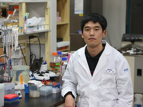
 Plasma, an Excellent Sterilizer to Remove Harmful Bacteria
(PhD candidate Joo Young Park, Professor Wonho Choe and PhD researcher Sanghoo Park)
KAIST researchers are using plasma to remove bacteria that are stuck to surfaces of plastic bottles and food. This novel technology will contribute to disinfection in medical settings as well as food and agricultural industries.
Professor Wonho Choe and his team from the Department of Physics developed a technology that removes biofilm, which is comprised of microorganisms, by using plasma as a non-thermal sterilization method.
Plasma contains multiple bactericidal agents, including reactive species. In particular, the chemicals formed in aqueous solution during plasma exposure have the potential for high antibacterial activity against various bacterial infections.
The team treated water with plasma to see how effectively bactericidal agents in the plasma water can remove biofilm comprised of harmful microorganism such as Escherichia coli, Salmonella, and Listeria.
The team identified that reactive species, including hydroxyl radical, hydrogen peroxide, ozone, nitrite, and superoxide produced during plasma treatment, showed considerable ability to remove the biofilm. Hydrogen peroxide showed the strongest effect removing the biofilm; however, the hydroxyl radical also played a significant role in removing biofilm. Despite having a concentration 100 to 10,000 times lower than other reactive species, the hydroxyl radical showed a high biofilm removal efficacy owing to its strong oxidative power.
These findings reveal that plasma can be used as a no-residual and safe sterilization process alternative to conventional methods. With these outcomes, the team is planning to develop and commercialize a technology that can produce hydroxyl radicals with plasma.
Professor Choe has registered a patent for flexible packaging materials that facilitate plasma and completed the technology transfer to the startup company, named ‘Plasmapp’, which focuses on commercializing bactericidal technology.
“This research outcome will be the foundation for understanding plasma control technology and physicochemical interactions between plasma and microorganisms. It will also become an accelerator for utilizing plasma technology in the medical, food, and agricultural fields,” said Professor Choe.
This research, led by PhD candidate Joo Young Park and PhD researcher Sanghoo Park in collaboration with Professor Cheorun Jo’s team from Seoul National University, was published in ACS Applied Materials and Interfaces on December 20, 2017.
Figure 1. Flexible packaging materials that facilitate plasma
Figure 2. Schematic diagram of biofilm treatment with plasma
Figure 3. Concept of plasma application and evaluation result of reactive species' efficacy
Figure 4. STERPACK, the product launched by Plasmapp
2018.01.25 View 11127
Plasma, an Excellent Sterilizer to Remove Harmful Bacteria
(PhD candidate Joo Young Park, Professor Wonho Choe and PhD researcher Sanghoo Park)
KAIST researchers are using plasma to remove bacteria that are stuck to surfaces of plastic bottles and food. This novel technology will contribute to disinfection in medical settings as well as food and agricultural industries.
Professor Wonho Choe and his team from the Department of Physics developed a technology that removes biofilm, which is comprised of microorganisms, by using plasma as a non-thermal sterilization method.
Plasma contains multiple bactericidal agents, including reactive species. In particular, the chemicals formed in aqueous solution during plasma exposure have the potential for high antibacterial activity against various bacterial infections.
The team treated water with plasma to see how effectively bactericidal agents in the plasma water can remove biofilm comprised of harmful microorganism such as Escherichia coli, Salmonella, and Listeria.
The team identified that reactive species, including hydroxyl radical, hydrogen peroxide, ozone, nitrite, and superoxide produced during plasma treatment, showed considerable ability to remove the biofilm. Hydrogen peroxide showed the strongest effect removing the biofilm; however, the hydroxyl radical also played a significant role in removing biofilm. Despite having a concentration 100 to 10,000 times lower than other reactive species, the hydroxyl radical showed a high biofilm removal efficacy owing to its strong oxidative power.
These findings reveal that plasma can be used as a no-residual and safe sterilization process alternative to conventional methods. With these outcomes, the team is planning to develop and commercialize a technology that can produce hydroxyl radicals with plasma.
Professor Choe has registered a patent for flexible packaging materials that facilitate plasma and completed the technology transfer to the startup company, named ‘Plasmapp’, which focuses on commercializing bactericidal technology.
“This research outcome will be the foundation for understanding plasma control technology and physicochemical interactions between plasma and microorganisms. It will also become an accelerator for utilizing plasma technology in the medical, food, and agricultural fields,” said Professor Choe.
This research, led by PhD candidate Joo Young Park and PhD researcher Sanghoo Park in collaboration with Professor Cheorun Jo’s team from Seoul National University, was published in ACS Applied Materials and Interfaces on December 20, 2017.
Figure 1. Flexible packaging materials that facilitate plasma
Figure 2. Schematic diagram of biofilm treatment with plasma
Figure 3. Concept of plasma application and evaluation result of reactive species' efficacy
Figure 4. STERPACK, the product launched by Plasmapp
2018.01.25 View 11127 -
 Lifespan of Fuel Cells Maximized Using Small Amount of Metals
(Professor Jung (far right) and his team)
Fuel cells are key future energy technology that is emerging as eco-friendly and renewable energy sources. In particular, solid oxide fuel cells composed of ceramic materials gain increasing attention for their ability to directly convert various forms of fuel such as biomass, LNG, and LPG to electric energy.
KAIST researchers described a new technique to improve chemical stability of electrode materials which can extend the lifespan by employing a very little amount of metals.
The core factor that determines the performance of solid oxide fuel cells is the cathode at which the reduction reaction of oxygen occurs. Conventionally, oxides with perovskite structure (ABO3) are used in cathodes. However, despite the high performance of perovskite oxides at initial operation, the performance decreases with time, limiting their long-term use. In particular, the condition of high temperature oxidation state required for cathode operation leads to surface segregation phenomenon, in which second phases such as strontium oxide (SrOx) accumulate on the surface of oxides, resulting in decrease in electrode performance. The detailed mechanism of this phenomenon and a way to effectively inhibit it has not been suggested.
Using computational chemistry and experimental data, Professor WooChul Jung’s team at the Department of Materials Science and Engineering observed that local compressive states around the Sr atoms in a perovskite electrode lattice weakened the Sr-O bond strength, which in turn promote strontium segregation. The team identified local changes in strain distribution in perovskite oxide as the main cause of segregation on strontium surface. Based on these findings, the team doped different sizes of metals in oxides to control the extent of lattice strain in cathode material and effectively inhibited strontium segregation.
Professor Jung said, “This technology can be implemented by adding a small amount of metal atoms during material synthesis, without any additional process.” He continued, “I hope this technology will be useful in developing high-durable perovskite oxide electrode in the future.”
The study co-led by Professor Jung and Professor Jeong Woo Han at Department of Chemical Engineering, University of Seoul was featured as the cover of Energy and Environmental Science in the first issue of 2018.
(Figure1.Correlation between the extent of lattice strain in electrode, strontium segregation, and electrode reaction.)
(Figure 2. Cathode surface of solid oxide fuel cell stabilized using the developed technology)
2018.01.18 View 9285
Lifespan of Fuel Cells Maximized Using Small Amount of Metals
(Professor Jung (far right) and his team)
Fuel cells are key future energy technology that is emerging as eco-friendly and renewable energy sources. In particular, solid oxide fuel cells composed of ceramic materials gain increasing attention for their ability to directly convert various forms of fuel such as biomass, LNG, and LPG to electric energy.
KAIST researchers described a new technique to improve chemical stability of electrode materials which can extend the lifespan by employing a very little amount of metals.
The core factor that determines the performance of solid oxide fuel cells is the cathode at which the reduction reaction of oxygen occurs. Conventionally, oxides with perovskite structure (ABO3) are used in cathodes. However, despite the high performance of perovskite oxides at initial operation, the performance decreases with time, limiting their long-term use. In particular, the condition of high temperature oxidation state required for cathode operation leads to surface segregation phenomenon, in which second phases such as strontium oxide (SrOx) accumulate on the surface of oxides, resulting in decrease in electrode performance. The detailed mechanism of this phenomenon and a way to effectively inhibit it has not been suggested.
Using computational chemistry and experimental data, Professor WooChul Jung’s team at the Department of Materials Science and Engineering observed that local compressive states around the Sr atoms in a perovskite electrode lattice weakened the Sr-O bond strength, which in turn promote strontium segregation. The team identified local changes in strain distribution in perovskite oxide as the main cause of segregation on strontium surface. Based on these findings, the team doped different sizes of metals in oxides to control the extent of lattice strain in cathode material and effectively inhibited strontium segregation.
Professor Jung said, “This technology can be implemented by adding a small amount of metal atoms during material synthesis, without any additional process.” He continued, “I hope this technology will be useful in developing high-durable perovskite oxide electrode in the future.”
The study co-led by Professor Jung and Professor Jeong Woo Han at Department of Chemical Engineering, University of Seoul was featured as the cover of Energy and Environmental Science in the first issue of 2018.
(Figure1.Correlation between the extent of lattice strain in electrode, strontium segregation, and electrode reaction.)
(Figure 2. Cathode surface of solid oxide fuel cell stabilized using the developed technology)
2018.01.18 View 9285 -
 Easier Way to Produce High Performing, Flexible Micro-Supercapacitor
(Professor Minyang Yang and PhD Student Jae Hak Lee)
Professor Minyang Yang from the Department of Mechanical Engineering and his team developed a high-energy, flexible micro-supercapacitor in a simple and cost-effective way.
Compared to conventional micro-batteries, such as lithium-ion batteries, these new batteries, also called supercapacitors, are significantly faster to charge and semi-permanent.
Thin, flexible micro-supercapacitors can be a power source directly attached to wearable and flexible electronics.
However, fabrication of these micro-supercapacitors requires a complex patterning process, such as lithography techniques and vacuum evaporation. Hence, the process requires expensive instruments and toxic chemicals.
To simplify the fabrication of micro-supercapacitors in an eco-friendly manner, the team developed laser growth sintering technology. This technology manufactures superporous silver electrodes and applies them to the supercapacitors’ electrodes.
The team used a laser to form micro-patterns and generated nanoporous structures inside. This laser-induced growth sintering contributed to shortening the manufacturing process from ten steps to one.
Moreover, the team explored this unique laser growth sintering process –nucleation, growth, and sintering –by employing a particle-free, organometallic solution, which is not costly compared to typical laser-sintering methods for metallic nanoparticle solutions used in the printing of micro-electrodes.
Finally, unlike the typical supercapacitors comprised of a single substance, the team applied an asymmetric electrode configuration of nanoporous gold and manganese dioxide, which exhibits a highly-specific capacitance, to operate at a high voltage.
This method allows the team to develop energy storage with a high capacity. This developed micro-supercapacitor only requires four seconds to be charged and passed more than 5,000 durability tests.
Professor Yang said, “This research outcome can be used as energy storage installed in wearable and flexible electronic devices. Through this research, we are one step closer to realizing a complete version of flexible electronic devices by incorporating a power supply.”
This research, led by PhD candidate Jae Hak Lee, was selected as the cover of Journal of Materials Chemistry A on December 21, 2017.
Figure 1. Cover of the Journal Materials Chemistry A
Figure 2. Manufactured micro-supercapacitor and its performance
Figure 3. Laser growth sintering mechanism
Figure 4. Structural change of the silver conductor according to the irradiated laser energy
2018.01.18 View 9184
Easier Way to Produce High Performing, Flexible Micro-Supercapacitor
(Professor Minyang Yang and PhD Student Jae Hak Lee)
Professor Minyang Yang from the Department of Mechanical Engineering and his team developed a high-energy, flexible micro-supercapacitor in a simple and cost-effective way.
Compared to conventional micro-batteries, such as lithium-ion batteries, these new batteries, also called supercapacitors, are significantly faster to charge and semi-permanent.
Thin, flexible micro-supercapacitors can be a power source directly attached to wearable and flexible electronics.
However, fabrication of these micro-supercapacitors requires a complex patterning process, such as lithography techniques and vacuum evaporation. Hence, the process requires expensive instruments and toxic chemicals.
To simplify the fabrication of micro-supercapacitors in an eco-friendly manner, the team developed laser growth sintering technology. This technology manufactures superporous silver electrodes and applies them to the supercapacitors’ electrodes.
The team used a laser to form micro-patterns and generated nanoporous structures inside. This laser-induced growth sintering contributed to shortening the manufacturing process from ten steps to one.
Moreover, the team explored this unique laser growth sintering process –nucleation, growth, and sintering –by employing a particle-free, organometallic solution, which is not costly compared to typical laser-sintering methods for metallic nanoparticle solutions used in the printing of micro-electrodes.
Finally, unlike the typical supercapacitors comprised of a single substance, the team applied an asymmetric electrode configuration of nanoporous gold and manganese dioxide, which exhibits a highly-specific capacitance, to operate at a high voltage.
This method allows the team to develop energy storage with a high capacity. This developed micro-supercapacitor only requires four seconds to be charged and passed more than 5,000 durability tests.
Professor Yang said, “This research outcome can be used as energy storage installed in wearable and flexible electronic devices. Through this research, we are one step closer to realizing a complete version of flexible electronic devices by incorporating a power supply.”
This research, led by PhD candidate Jae Hak Lee, was selected as the cover of Journal of Materials Chemistry A on December 21, 2017.
Figure 1. Cover of the Journal Materials Chemistry A
Figure 2. Manufactured micro-supercapacitor and its performance
Figure 3. Laser growth sintering mechanism
Figure 4. Structural change of the silver conductor according to the irradiated laser energy
2018.01.18 View 9184 -
 Professor Jung Awarded the Pople Medal by the APATCC
(Professor Yousung Jung)
Professor Yousung Jung of the Graduate School of EEWS won the Pople Medal from the Asia-Pacific Association of Theoretical & Computational Chemists (APATCC).
The Pople Medal has been awarded annually since 2007 to recognize young scholars in the fields of theoretical/computational chemistry in honor of Sir John Anthony Pople, who passed away in 2004. Dr. Pople was a British theoretical chemist and a Nobel laureate in 1998 for his development of computational methods in quantum chemistry.
The Pople Medal is awarded to scientists at or under the age of 45 in the Asia-Pacific region who have distinguished themselves through pioneering and important contributions.
Professor Jung was honored for his outstanding contributions to developing efficient electronic structure methods and their applications to energy materials discovery. He has published more than 120 papers in prestigious academic journals. He also has an h-index of 44, and has been cited more than 8,000 times.
2018.01.10 View 8957
Professor Jung Awarded the Pople Medal by the APATCC
(Professor Yousung Jung)
Professor Yousung Jung of the Graduate School of EEWS won the Pople Medal from the Asia-Pacific Association of Theoretical & Computational Chemists (APATCC).
The Pople Medal has been awarded annually since 2007 to recognize young scholars in the fields of theoretical/computational chemistry in honor of Sir John Anthony Pople, who passed away in 2004. Dr. Pople was a British theoretical chemist and a Nobel laureate in 1998 for his development of computational methods in quantum chemistry.
The Pople Medal is awarded to scientists at or under the age of 45 in the Asia-Pacific region who have distinguished themselves through pioneering and important contributions.
Professor Jung was honored for his outstanding contributions to developing efficient electronic structure methods and their applications to energy materials discovery. He has published more than 120 papers in prestigious academic journals. He also has an h-index of 44, and has been cited more than 8,000 times.
2018.01.10 View 8957 -
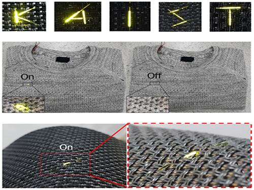 Fiber OLEDs, Thinner Than a Hair
(Seonil Kwon, PhD Candidate)
Professor Kyung Cheol Choi from the School of Electrical Engineering and his team succeeded in fabricating highly efficient Organic Light-Emitting Diodes (OLEDs) on an ultra-thin fiber.
The team expects the technology, which produces high-efficiency, long-lasting OLEDs, can be widely utilized in wearable displays.
Existing fiber-based wearable displays’ OLEDs show much lower performance compared to those fabricated on planar substrates. This low performance caused a limitation for applying it to actual wearable displays.
In order to solve this problem, the team designed a structure of OLEDs compatible to fiber and used a dip-coating method in a three-dimensional structure of fibers. Through this method, the team successfully developed efficient OLEDs that are designed to last a lifetime and are still equivalent to those on planar substrates.
The team identified that solution process planar OLEDs can be applied to fibers without any reduction in performance through the technology. This fiber OLEDs exhibited luminance and current efficiency values of over 10,000 cd/m^2(candela/square meter) and 11 cd/A (candela/ampere).
The team also verified that the fiber OLEDs withstood tensile strains of up to 4.3% while retaining more than 90% of their current efficiency. In addition, they could be woven into textiles and knitted clothes without causing any problems.
Moreover, the technology allows for fabricating OLEDs on fibers with diameters ranging from 300㎛ down to 90㎛, thinner than a human hair, which attests to the scalability of the proposed fabrication scheme.
Noting that every process is carried out at a low temperature (~105℃), fibers vulnerable to high temperatures can also employ this fabrication scheme.
Professor Choi said, “Existing fiber-based wearable displays had limitations for applicability due to their low performance. However, this technology can fabricate OLEDs with high performance on fibers. This simple, low-cost process opens a way to commercialize fiber-based wearable displays.”
This research led by a PhD candidate Seonil Kwon was published online in the international journal for nanoscience, Nano Letters, on December 6.
(Fiber-based OLEDs woven into knitted clothes)
This work was funded by the Engineering Research Center of Excellence Program (Grant No. NRF-2017R1A5A1014708) and Nano-Material Technology Development Program (Grant No. NRF-2016M3A7B4910635) by the National Research Foundation of Korea, the Ministry of Science and ICT of Korea.
2018.01.09 View 14857
Fiber OLEDs, Thinner Than a Hair
(Seonil Kwon, PhD Candidate)
Professor Kyung Cheol Choi from the School of Electrical Engineering and his team succeeded in fabricating highly efficient Organic Light-Emitting Diodes (OLEDs) on an ultra-thin fiber.
The team expects the technology, which produces high-efficiency, long-lasting OLEDs, can be widely utilized in wearable displays.
Existing fiber-based wearable displays’ OLEDs show much lower performance compared to those fabricated on planar substrates. This low performance caused a limitation for applying it to actual wearable displays.
In order to solve this problem, the team designed a structure of OLEDs compatible to fiber and used a dip-coating method in a three-dimensional structure of fibers. Through this method, the team successfully developed efficient OLEDs that are designed to last a lifetime and are still equivalent to those on planar substrates.
The team identified that solution process planar OLEDs can be applied to fibers without any reduction in performance through the technology. This fiber OLEDs exhibited luminance and current efficiency values of over 10,000 cd/m^2(candela/square meter) and 11 cd/A (candela/ampere).
The team also verified that the fiber OLEDs withstood tensile strains of up to 4.3% while retaining more than 90% of their current efficiency. In addition, they could be woven into textiles and knitted clothes without causing any problems.
Moreover, the technology allows for fabricating OLEDs on fibers with diameters ranging from 300㎛ down to 90㎛, thinner than a human hair, which attests to the scalability of the proposed fabrication scheme.
Noting that every process is carried out at a low temperature (~105℃), fibers vulnerable to high temperatures can also employ this fabrication scheme.
Professor Choi said, “Existing fiber-based wearable displays had limitations for applicability due to their low performance. However, this technology can fabricate OLEDs with high performance on fibers. This simple, low-cost process opens a way to commercialize fiber-based wearable displays.”
This research led by a PhD candidate Seonil Kwon was published online in the international journal for nanoscience, Nano Letters, on December 6.
(Fiber-based OLEDs woven into knitted clothes)
This work was funded by the Engineering Research Center of Excellence Program (Grant No. NRF-2017R1A5A1014708) and Nano-Material Technology Development Program (Grant No. NRF-2016M3A7B4910635) by the National Research Foundation of Korea, the Ministry of Science and ICT of Korea.
2018.01.09 View 14857 -
 Ultra-Low Power Flexible Memory Using 2D Materials
(Professor Choi and Ph.D. candidate Jang)
KAIST research team led by Professor Sung-Yool Choi at School of Electrical Engineering and Professor Sung Gap Im at the Department of Chemical and Biomolecular Engineering developed high-density, ultra-low power, non-volatile, flexible memory technology using 2D materials. The team used ultrathin molybdenum disulfide (MoS2) with atomic-scale thickness as the channel material and high-performance polymeric insulator film as the tunneling dielectric material. This research was published on the cover of Advanced Functional Materials on November 17. KAIST graduate Myung Hun Woo, a researcher at Samsung Electronics and Ph.D. candidate Byung Chul Jang are first authors.
The surge of new technologies such as Internet of Things (IoT), Artificial Intelligence (AI), and cloud server led to the paradigm shift from processor-centric computing to memory-centric computing in the industry, as well as the increase in demand of wearable devices. This led to an increased need for high-density, ultra-low power, non-volatile flexible memory. In particular, ultrathin MoS2 as semiconductor material has been recently regarded as post-silicon material. This is due to its ultrathin thickness of atomic-scale which suppresses short channel effect observed in conventional silicon material, leading to advantages in high- density and low-power consumption. Further, this thickness allows the material to be flexible, and thus the material is applicable to wearable devices.
However, due to the dangling-bond free surface of MoS2 semiconductor material, it is difficult to deposit the thin insulator film to be uniform and stable over a large area via the conventional atomic layer deposition process. Further, the currently used solution process makes it difficult to deposit uniformly low dielectric constant (k) polymeric insulator film with sub-10 nm thickness on a large area, thus indicating that the memory device utilizing the conventional solution-processed polymer insulator film cannot be operated at low-operating voltage and is not compatible with photolithography.
The research team tried to overcome the hurdles and develop high-density, ultra-low power, non-volatile flexible memory by employing a low-temperature, solvent-free, and all-dry vapor phase technique named initiated chemical vapor deposition (iCVD) process. Using iCVD process, tunneling polymeric insulator film with 10 nm thickness was deposited uniformly on MoS2 semiconductor material without being restricted by the dangling bond-free surface of MoS2. The team observed that the newly developed MoS2-based non-volatile memory can be operated at low-voltage (around 10V), in contrast to the conventional MoS2-based non-volatile memory that requires over 20V.
Professor Choi said, “As the basis for the Fourth Industrial revolution technologies including AI and IoT, semiconductor device technology needs to have characteristics of low-power and flexibility, in clear contrast to conventional memory devices.” He continued, “This new technology is significant in developing source technology in terms of materials, processes, and devices to contribute to achieve these characteristics.”
This research was supported by the Global Frontier Center for Advanced Soft Electronics and the Creative Materials Discovery Program by funded the National Research Foundation of Korea of Ministry of Science and ICT.
( Figure 1. Cover of Advanced Functional Materials)
(Figure 2. Concept map for the developed non-volatile memory material and high-resolution transmission electron microscopy image for material cross-section )
2018.01.02 View 11045
Ultra-Low Power Flexible Memory Using 2D Materials
(Professor Choi and Ph.D. candidate Jang)
KAIST research team led by Professor Sung-Yool Choi at School of Electrical Engineering and Professor Sung Gap Im at the Department of Chemical and Biomolecular Engineering developed high-density, ultra-low power, non-volatile, flexible memory technology using 2D materials. The team used ultrathin molybdenum disulfide (MoS2) with atomic-scale thickness as the channel material and high-performance polymeric insulator film as the tunneling dielectric material. This research was published on the cover of Advanced Functional Materials on November 17. KAIST graduate Myung Hun Woo, a researcher at Samsung Electronics and Ph.D. candidate Byung Chul Jang are first authors.
The surge of new technologies such as Internet of Things (IoT), Artificial Intelligence (AI), and cloud server led to the paradigm shift from processor-centric computing to memory-centric computing in the industry, as well as the increase in demand of wearable devices. This led to an increased need for high-density, ultra-low power, non-volatile flexible memory. In particular, ultrathin MoS2 as semiconductor material has been recently regarded as post-silicon material. This is due to its ultrathin thickness of atomic-scale which suppresses short channel effect observed in conventional silicon material, leading to advantages in high- density and low-power consumption. Further, this thickness allows the material to be flexible, and thus the material is applicable to wearable devices.
However, due to the dangling-bond free surface of MoS2 semiconductor material, it is difficult to deposit the thin insulator film to be uniform and stable over a large area via the conventional atomic layer deposition process. Further, the currently used solution process makes it difficult to deposit uniformly low dielectric constant (k) polymeric insulator film with sub-10 nm thickness on a large area, thus indicating that the memory device utilizing the conventional solution-processed polymer insulator film cannot be operated at low-operating voltage and is not compatible with photolithography.
The research team tried to overcome the hurdles and develop high-density, ultra-low power, non-volatile flexible memory by employing a low-temperature, solvent-free, and all-dry vapor phase technique named initiated chemical vapor deposition (iCVD) process. Using iCVD process, tunneling polymeric insulator film with 10 nm thickness was deposited uniformly on MoS2 semiconductor material without being restricted by the dangling bond-free surface of MoS2. The team observed that the newly developed MoS2-based non-volatile memory can be operated at low-voltage (around 10V), in contrast to the conventional MoS2-based non-volatile memory that requires over 20V.
Professor Choi said, “As the basis for the Fourth Industrial revolution technologies including AI and IoT, semiconductor device technology needs to have characteristics of low-power and flexibility, in clear contrast to conventional memory devices.” He continued, “This new technology is significant in developing source technology in terms of materials, processes, and devices to contribute to achieve these characteristics.”
This research was supported by the Global Frontier Center for Advanced Soft Electronics and the Creative Materials Discovery Program by funded the National Research Foundation of Korea of Ministry of Science and ICT.
( Figure 1. Cover of Advanced Functional Materials)
(Figure 2. Concept map for the developed non-volatile memory material and high-resolution transmission electron microscopy image for material cross-section )
2018.01.02 View 11045 -
 Non-Adiabatic Reaction Mechanism Identified at Conical Intersection
(Professor Kim(center) and Ph.D. candidates Kyung Chul Woo (left) and Kang Do Hyung)
Research team led by Professor Sang Kyu Kim at KAIST Department of Chemistry observed two distinct reaction pathways that occur at conical intersection where two different adiabatic potential energy surfaces cross at the same nuclear configuration.
Professor Kim previously identified the existence and molecular structure of conical intersection in 2010. In this following study, the team accurately measured reaction rates of two totally different reaction pathways activated only at conical intersection where the seminal Born-Oppenheimer approximation breaks down.
This study led by Kyung Chul Woo (1st author) and Do Hyung Kang, both Ph.D. candidates at KAIST, was published in Journal of the American Chemical Society in November 7th, 2017.
Chemical reaction induced by light occurs in excited electronic states where the reaction outcome is often destined by coupling among different electronic states mediated by nuclear motions during chemical reaction. Such a coupling is most critical and important at the conical intersection as nonadiabtic surface-hopping is most probable at situation where the Born-Oppenheimer approximation fails.
Professor Kim used spectroscopic methods in 2010 to experimentally observe conical intersection of polyatomic molecule. And yet, it was not possible to disentangle complex dynamic processes with frequency-domain study only.
The research team used pico-second time-resolution kinetic energy resolved mass spectrometry to identify two possible distinct reaction pathways in both energy and time domains.,.
The research team demonstrated that the reactive flux prepared at the conical intersection is bifurcated into adiabatic or non-adiabatic reaction pathways. These two pathways are quite distinct in terms of reaction rates, energy releases, and product branching ratios.
This is the first study to capture the moment of bifurcation dynamics at the conical intersection for complex polyatomic molecular system. The study could contribute to conceptual improvement in understanding complicated nonadiabatic dynamics in general.
Professor Kim said, “Basic science research is essential in understanding and wisely using the nature. New technological advances cannot be made without the advancement in basic science.” He continued, “I hope this study could lead to growth in many young academic talents in basic sciences.”
(Figure 1. Reaction graph starting from reaction intersection that divides into adiabatic reaction pathway (red) and non-adiabatic pathway (blue))
2017.12.19 View 7286
Non-Adiabatic Reaction Mechanism Identified at Conical Intersection
(Professor Kim(center) and Ph.D. candidates Kyung Chul Woo (left) and Kang Do Hyung)
Research team led by Professor Sang Kyu Kim at KAIST Department of Chemistry observed two distinct reaction pathways that occur at conical intersection where two different adiabatic potential energy surfaces cross at the same nuclear configuration.
Professor Kim previously identified the existence and molecular structure of conical intersection in 2010. In this following study, the team accurately measured reaction rates of two totally different reaction pathways activated only at conical intersection where the seminal Born-Oppenheimer approximation breaks down.
This study led by Kyung Chul Woo (1st author) and Do Hyung Kang, both Ph.D. candidates at KAIST, was published in Journal of the American Chemical Society in November 7th, 2017.
Chemical reaction induced by light occurs in excited electronic states where the reaction outcome is often destined by coupling among different electronic states mediated by nuclear motions during chemical reaction. Such a coupling is most critical and important at the conical intersection as nonadiabtic surface-hopping is most probable at situation where the Born-Oppenheimer approximation fails.
Professor Kim used spectroscopic methods in 2010 to experimentally observe conical intersection of polyatomic molecule. And yet, it was not possible to disentangle complex dynamic processes with frequency-domain study only.
The research team used pico-second time-resolution kinetic energy resolved mass spectrometry to identify two possible distinct reaction pathways in both energy and time domains.,.
The research team demonstrated that the reactive flux prepared at the conical intersection is bifurcated into adiabatic or non-adiabatic reaction pathways. These two pathways are quite distinct in terms of reaction rates, energy releases, and product branching ratios.
This is the first study to capture the moment of bifurcation dynamics at the conical intersection for complex polyatomic molecular system. The study could contribute to conceptual improvement in understanding complicated nonadiabatic dynamics in general.
Professor Kim said, “Basic science research is essential in understanding and wisely using the nature. New technological advances cannot be made without the advancement in basic science.” He continued, “I hope this study could lead to growth in many young academic talents in basic sciences.”
(Figure 1. Reaction graph starting from reaction intersection that divides into adiabatic reaction pathway (red) and non-adiabatic pathway (blue))
2017.12.19 View 7286 -
 Technology Detecting RNase Activity
(Ph.D. candidate Chang Yeol Lee)
A KAIST research team of Professor Hyun Gyu Park at Department of Chemical and Biomolecular Engineering developed a new technology to detect the activity of RNase H, a RNA degrading enzyme. The team used highly efficient signal amplification reaction termed catalytic hairpin assembly (CHA) to effectively analyze the RNase H activity. Considering that RNase H is required in the proliferation of retroviruses such as HIV, this research finding could contribute to AIDS treatments in the future, researchers say.
This study led by Ph.D. candidates Chang Yeol Lee and Hyowon Jang was chosen as the cover for Nanoscale (Issue 42, 2017) published in 14 November.
The existing techniques to detect RNase H require expensive fluorophore and quencher, and involve complex implementation. Further, there is no way to amplify the signal, leading to low detection efficiency overall. The team utilized CHA technology to overcome these limitations. CHA amplifies detection signal to allow more sensitive RNase H activity assay.
The team designed the reaction system so that the product of CHA reaction has G-quadruplex structures, which is suitable to generate fluorescence. By using fluorescent molecules that bind to G-quadruplexes to generate strong fluorescence, the team could develop high performance RNase H detection method that overcomes the limitations of existing techniques. Further, this technology could screen inhibitors of RNase H activity.
The team expects that the research finding could contribute to AIDS treatment. AIDS is disease caused by HIV, a retrovirus that utilizes reverse transcription, during which RNA is converted to DNA. RNase H is essential for reverse transcription in HIV, and thus inhibition of RNase H could in turn inhibit transcription of HIV DNA.
Professor Park said, “This technology is applicable to detect various enzyme activities, as well as RNase H activity.” He continued, “I hope this technology could be widely used in research on enzyme related diseases.”
This study was funded by Global Frontier project and Mid-career Researcher Support project of the Ministry of Science and ICT.
2017.11.28 View 7751
Technology Detecting RNase Activity
(Ph.D. candidate Chang Yeol Lee)
A KAIST research team of Professor Hyun Gyu Park at Department of Chemical and Biomolecular Engineering developed a new technology to detect the activity of RNase H, a RNA degrading enzyme. The team used highly efficient signal amplification reaction termed catalytic hairpin assembly (CHA) to effectively analyze the RNase H activity. Considering that RNase H is required in the proliferation of retroviruses such as HIV, this research finding could contribute to AIDS treatments in the future, researchers say.
This study led by Ph.D. candidates Chang Yeol Lee and Hyowon Jang was chosen as the cover for Nanoscale (Issue 42, 2017) published in 14 November.
The existing techniques to detect RNase H require expensive fluorophore and quencher, and involve complex implementation. Further, there is no way to amplify the signal, leading to low detection efficiency overall. The team utilized CHA technology to overcome these limitations. CHA amplifies detection signal to allow more sensitive RNase H activity assay.
The team designed the reaction system so that the product of CHA reaction has G-quadruplex structures, which is suitable to generate fluorescence. By using fluorescent molecules that bind to G-quadruplexes to generate strong fluorescence, the team could develop high performance RNase H detection method that overcomes the limitations of existing techniques. Further, this technology could screen inhibitors of RNase H activity.
The team expects that the research finding could contribute to AIDS treatment. AIDS is disease caused by HIV, a retrovirus that utilizes reverse transcription, during which RNA is converted to DNA. RNase H is essential for reverse transcription in HIV, and thus inhibition of RNase H could in turn inhibit transcription of HIV DNA.
Professor Park said, “This technology is applicable to detect various enzyme activities, as well as RNase H activity.” He continued, “I hope this technology could be widely used in research on enzyme related diseases.”
This study was funded by Global Frontier project and Mid-career Researcher Support project of the Ministry of Science and ICT.
2017.11.28 View 7751 -
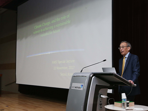 Dr. Steven Chu Talks on Sustainable Energy Policy at KAIST
Nobel Laureate in physics and former US Energy Secretary Steven Chu called for concerted efforts to develop a more sustainable energy policy and portfolio at a lecture held at KAIST and a forum in Seoul on November 23.
A policy with an energy mix including nuclear power and renewable energy could be ideal for retaining a stable energy supply given Korea’s very limited geographical conditions, Chu said during the Future Energy Forum in Seoul. He also held a lecture at KAIST’s Daejeon campus on “Climate Change, the Importance of Science and Policy in Achieving a Sustainable Future.”
He said that unlike the United States, Korea and Japan have geographical limitations for generating enough renewable energy. "Wind speeds of more than 10 meters per second would allow wind power generation, but, South Korea's southernmost wind speed in Jeju is less than 8 meters per second, and the amount of sunshine is lower than in the Middle East. It is ideal to combine renewable energy with nuclear power plants," he said.
Chu also stressed the role of science in achieving a sustainable future, citing many cases in foreign countries. For instance, Germany once decided to do away with nuclear power. However, their initial plan does not directly raise energy efficiency and the proportion of fossil fuels has led to an increase in the environmental issue of fine particular matter as well as carbon dioxide emission increases.
He said that in the long term, renewable energy will emerge as major alternative resources, stressing the role of science in achieving a sustainable future. Without this alternative, we will eventually burn more fossil fuels and pollute the air.
Chu also said that nuclear waste and safe plant operation will be a big concern, but it is technologically viable since Korea has already proven its prowess in nuclear power plant building and safety technology.
Chu added, "Research in chemical energy storage through novel electrochemistry may lead to solutions, but for the next half century we will need additional energy-on-demand and carbon-free sources of energy from proven technologies."
"While science, innovation and technology will no doubt lead to better solutions, sound government policies are needed to advance the transition to carbon-free energy needed to achieve a more sustainable world," he said.
After serving as the US Secretary of Energy for four years from 2009 to 2013, Professor Chu returned to Stanford University, and currently holds a position of the William R. Kenan, Jr. Professor of Physics as well as Professor in the Department of Molecular and Cellular Physiology.
Professor Chu is known for his research at Bell Labs and Stanford University regarding the cooling and trapping of atoms with laser light, for which he won the Nobel Prize in Physics in 1997.
2017.11.24 View 5935
Dr. Steven Chu Talks on Sustainable Energy Policy at KAIST
Nobel Laureate in physics and former US Energy Secretary Steven Chu called for concerted efforts to develop a more sustainable energy policy and portfolio at a lecture held at KAIST and a forum in Seoul on November 23.
A policy with an energy mix including nuclear power and renewable energy could be ideal for retaining a stable energy supply given Korea’s very limited geographical conditions, Chu said during the Future Energy Forum in Seoul. He also held a lecture at KAIST’s Daejeon campus on “Climate Change, the Importance of Science and Policy in Achieving a Sustainable Future.”
He said that unlike the United States, Korea and Japan have geographical limitations for generating enough renewable energy. "Wind speeds of more than 10 meters per second would allow wind power generation, but, South Korea's southernmost wind speed in Jeju is less than 8 meters per second, and the amount of sunshine is lower than in the Middle East. It is ideal to combine renewable energy with nuclear power plants," he said.
Chu also stressed the role of science in achieving a sustainable future, citing many cases in foreign countries. For instance, Germany once decided to do away with nuclear power. However, their initial plan does not directly raise energy efficiency and the proportion of fossil fuels has led to an increase in the environmental issue of fine particular matter as well as carbon dioxide emission increases.
He said that in the long term, renewable energy will emerge as major alternative resources, stressing the role of science in achieving a sustainable future. Without this alternative, we will eventually burn more fossil fuels and pollute the air.
Chu also said that nuclear waste and safe plant operation will be a big concern, but it is technologically viable since Korea has already proven its prowess in nuclear power plant building and safety technology.
Chu added, "Research in chemical energy storage through novel electrochemistry may lead to solutions, but for the next half century we will need additional energy-on-demand and carbon-free sources of energy from proven technologies."
"While science, innovation and technology will no doubt lead to better solutions, sound government policies are needed to advance the transition to carbon-free energy needed to achieve a more sustainable world," he said.
After serving as the US Secretary of Energy for four years from 2009 to 2013, Professor Chu returned to Stanford University, and currently holds a position of the William R. Kenan, Jr. Professor of Physics as well as Professor in the Department of Molecular and Cellular Physiology.
Professor Chu is known for his research at Bell Labs and Stanford University regarding the cooling and trapping of atoms with laser light, for which he won the Nobel Prize in Physics in 1997.
2017.11.24 View 5935 -
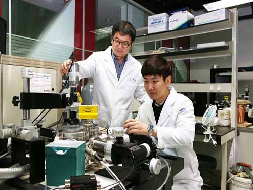
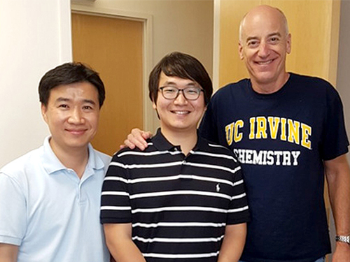 Ultra-Fast and Ultra-Sensitive Hydrogen Sensor
(From left: Professor Kim, Ph.D. candidate Koo, and Professor Penner)
A KAIST team made an ultra-fast hydrogen sensor that can detect hydrogen gas levels under 1% in less than seven seconds. The sensor also can detect hundreds of parts per million levels of hydrogen gas within 60 seconds at room temperature.
A research group under Professor Il-Doo Kim in the Department of Materials Science and Engineering at KAIST, in collaboration with Professor Reginald M. Penner of the University of California-Irvine, has developed an ultra-fast hydrogen gas detection system based on a palladium (Pd) nanowire array coated with a metal-organic framework (MOF).
Hydrogen has been regarded as an eco-friendly next-generation energy source. However, it is a flammable gas that can explode even with a small spark. For safety, the lower explosion limit for hydrogen gas is 4 vol% so sensors should be able to detect the colorless and odorless hydrogen molecule quickly. The importance of sensors capable of rapidly detecting colorless and odorless hydrogen gas has been emphasized in recent guidelines issued by the U.S. Department of Energy. According to the guidelines, hydrogen sensors should detect 1 vol% of hydrogen in air in less than 60 seconds for adequate response and recovery times.
To overcome the limitations of Pd-based hydrogen sensors, the research team introduced a MOF layer on top of a Pd nanowire array. Lithographically patterned Pd nanowires were simply overcoated with a Zn-based zeolite imidazole framework (ZIF-8) layer composed of Zn ions and organic ligands. ZIF-8 film is easily coated on Pd nanowires by simple dipping (for 2–6 hours) in a methanol solution including Zn (NO3)2·6H2O and 2-methylimidazole.
(This cover image depicts lithographically-patterned Pd nanowires overcoated with a Zn-based zeolite imidazole framework (ZIF-8) layer.)
As synthesized ZIF-8 is a highly porous material composed of a number of micro-pores of 0.34 nm and 1.16 nm, hydrogen gas with a kinetic diameter of 0.289 nm can easily penetrate inside the ZIF-8 membrane, while large molecules (> 0.34 nm) are effectively screened by the MOF filter. Thus, the ZIF-8 filter on the Pd nanowires allows the predominant penetration of hydrogen molecules, leading to the acceleration of Pd-based H2 sensors with a 20-fold faster recovery and response speed compared to pristine Pd nanowires at room temperature.
Professor Kim expects that the ultra-fast hydrogen sensor can be useful for the prevention of explosion accidents caused by the leakage of hydrogen gas. In addition, he expects that other harmful gases in the air can be accurately detected through effective nano-filtration by using of a variety of MOF layers.
This study was carried out by Ph.D. candidate Won-Tae Koo (first author), Professor Kim (co-corresponding author), and Professor Penner (co-corresponding author). The study has been published in the online edition of ACS Nano, as the cover-featured image for the September issue.
Figure 1. Representative image for this paper published in ACS Nano, August, 18.
Figure 2. Images of Pd nanowire array-based hydrogen sensors, scanning electron microscopy image of a Pd nanowire covered by a metal-organic framework layer, and the hydrogen sensing properties of the sensors.
Figure 3. Schematic illustration of a metal-organic framework (MOF). The MOF, consisting of metal ions and organic ligands, is a highly porous material with an ultrahigh surface area. The various structures of MOFs can be synthesized depending on the kinds of metal ions and organic ligands.
2017.09.28 View 12161
Ultra-Fast and Ultra-Sensitive Hydrogen Sensor
(From left: Professor Kim, Ph.D. candidate Koo, and Professor Penner)
A KAIST team made an ultra-fast hydrogen sensor that can detect hydrogen gas levels under 1% in less than seven seconds. The sensor also can detect hundreds of parts per million levels of hydrogen gas within 60 seconds at room temperature.
A research group under Professor Il-Doo Kim in the Department of Materials Science and Engineering at KAIST, in collaboration with Professor Reginald M. Penner of the University of California-Irvine, has developed an ultra-fast hydrogen gas detection system based on a palladium (Pd) nanowire array coated with a metal-organic framework (MOF).
Hydrogen has been regarded as an eco-friendly next-generation energy source. However, it is a flammable gas that can explode even with a small spark. For safety, the lower explosion limit for hydrogen gas is 4 vol% so sensors should be able to detect the colorless and odorless hydrogen molecule quickly. The importance of sensors capable of rapidly detecting colorless and odorless hydrogen gas has been emphasized in recent guidelines issued by the U.S. Department of Energy. According to the guidelines, hydrogen sensors should detect 1 vol% of hydrogen in air in less than 60 seconds for adequate response and recovery times.
To overcome the limitations of Pd-based hydrogen sensors, the research team introduced a MOF layer on top of a Pd nanowire array. Lithographically patterned Pd nanowires were simply overcoated with a Zn-based zeolite imidazole framework (ZIF-8) layer composed of Zn ions and organic ligands. ZIF-8 film is easily coated on Pd nanowires by simple dipping (for 2–6 hours) in a methanol solution including Zn (NO3)2·6H2O and 2-methylimidazole.
(This cover image depicts lithographically-patterned Pd nanowires overcoated with a Zn-based zeolite imidazole framework (ZIF-8) layer.)
As synthesized ZIF-8 is a highly porous material composed of a number of micro-pores of 0.34 nm and 1.16 nm, hydrogen gas with a kinetic diameter of 0.289 nm can easily penetrate inside the ZIF-8 membrane, while large molecules (> 0.34 nm) are effectively screened by the MOF filter. Thus, the ZIF-8 filter on the Pd nanowires allows the predominant penetration of hydrogen molecules, leading to the acceleration of Pd-based H2 sensors with a 20-fold faster recovery and response speed compared to pristine Pd nanowires at room temperature.
Professor Kim expects that the ultra-fast hydrogen sensor can be useful for the prevention of explosion accidents caused by the leakage of hydrogen gas. In addition, he expects that other harmful gases in the air can be accurately detected through effective nano-filtration by using of a variety of MOF layers.
This study was carried out by Ph.D. candidate Won-Tae Koo (first author), Professor Kim (co-corresponding author), and Professor Penner (co-corresponding author). The study has been published in the online edition of ACS Nano, as the cover-featured image for the September issue.
Figure 1. Representative image for this paper published in ACS Nano, August, 18.
Figure 2. Images of Pd nanowire array-based hydrogen sensors, scanning electron microscopy image of a Pd nanowire covered by a metal-organic framework layer, and the hydrogen sensing properties of the sensors.
Figure 3. Schematic illustration of a metal-organic framework (MOF). The MOF, consisting of metal ions and organic ligands, is a highly porous material with an ultrahigh surface area. The various structures of MOFs can be synthesized depending on the kinds of metal ions and organic ligands.
2017.09.28 View 12161