materials
-
 A Molecular Switch Controlling Self-Assembly of Protein Nanotubes Discovered
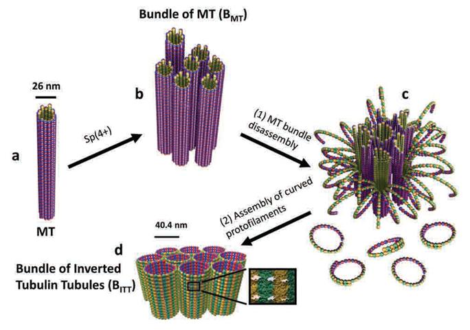
International collaborative research among South Korea, United States, and Israel research institutionsThe key to the treatment of cancer and brain disease mechanism The molecular switch that controls the self-assembly structure of the protein nanotubes, which plays crucial role in cell division and intracellular transport of materials, has been discovered. KAIST Bio and Brain Engineering Department’s Professor Myeong-Cheol Choi and Professor Chae-Yeon Song conducted the research, in collaboration with the University of California in Santa Barbara, U.S., and Hebrew University in Israel. The findings of the research were published in Nature Materials on the 19th. Microtubules are tube shaped and composed of protein that plays a key role in cell division, cytoskeleton, and intercellular material transport and is only 25nm in diameter (1/100,000 thickness of a human hair). Conventionally, cancer treatment focused on disrupting the formation of microtubules to suppress the division of cancer cells. In addition Alzheimer’s is known to be caused by the diminishing of structural integrity of microtubules responsible for intercellular material transport which leads to failure in signal transfer. The research team utilized synchrotron x-ray scattering and transmission electron microscope to analyze the self assemble structure of protein nanotubes to subnanometer accuracy. As a result, the microtubules were found to assemble into 25nm thickness tubules by stacking protein blocks 4 x 5 x 8nm in dimension. In the process, the research team discovered the molecular switch that controls the shape of these protein blocks. In addition the research team was successful in creating a new protein tube structure. Professor Choi commented that they were successful in introducing a new paradigm that suggests the possibility of controlling the complex biological functions of human’s biological system with the simple use of physical principles. He commented further that it is anticipated that the findings will allow for the application of bio nanotubes in engineering and that this is a small step in finding the mechanism behind cancer treatment and neural diseases.
2014.02.03 View 12252
A Molecular Switch Controlling Self-Assembly of Protein Nanotubes Discovered
International collaborative research among South Korea, United States, and Israel research institutionsThe key to the treatment of cancer and brain disease mechanism The molecular switch that controls the self-assembly structure of the protein nanotubes, which plays crucial role in cell division and intracellular transport of materials, has been discovered. KAIST Bio and Brain Engineering Department’s Professor Myeong-Cheol Choi and Professor Chae-Yeon Song conducted the research, in collaboration with the University of California in Santa Barbara, U.S., and Hebrew University in Israel. The findings of the research were published in Nature Materials on the 19th. Microtubules are tube shaped and composed of protein that plays a key role in cell division, cytoskeleton, and intercellular material transport and is only 25nm in diameter (1/100,000 thickness of a human hair). Conventionally, cancer treatment focused on disrupting the formation of microtubules to suppress the division of cancer cells. In addition Alzheimer’s is known to be caused by the diminishing of structural integrity of microtubules responsible for intercellular material transport which leads to failure in signal transfer. The research team utilized synchrotron x-ray scattering and transmission electron microscope to analyze the self assemble structure of protein nanotubes to subnanometer accuracy. As a result, the microtubules were found to assemble into 25nm thickness tubules by stacking protein blocks 4 x 5 x 8nm in dimension. In the process, the research team discovered the molecular switch that controls the shape of these protein blocks. In addition the research team was successful in creating a new protein tube structure. Professor Choi commented that they were successful in introducing a new paradigm that suggests the possibility of controlling the complex biological functions of human’s biological system with the simple use of physical principles. He commented further that it is anticipated that the findings will allow for the application of bio nanotubes in engineering and that this is a small step in finding the mechanism behind cancer treatment and neural diseases.
2014.02.03 View 12252 -
 Rechargeable Lithium Sulfur Battery for Greater Battery Capacity
Professor Do Kyung Kim from the Department of Material Science and Engineering and Professor Jang Wook Choi from the Graduate School of EEWS have been featured in the lead story of the renowned nanoscience journal Advanced Materials for their research on the lithium sulfur battery. This new type of battery developed by Professor Kim is expected to have a longer life battery life and [higher] energy density than currently commercial batteries.
With ample energy density up to 2100Wh/kg—almost 5.4 times that of lithium ion batteries—lithium sulfur batteries can withstand the sharp decrease in energy capacity resulting from charging and discharging—which has been considered the inherent limitation of the conventional batteries.
Professor Kim and his research team used one-dimensional, vertical alignment of 75nm tick, 15μm long sulfur nanowires to maximize electric conductivity. Then, to prevent loss of battery life, they carbon-coated each nanowire and prohibited direct contact between the sulfur and electrolyte.
The result was one of the most powerful batteries in terms of both energy performance and density. Compared to conventional batteries which suffer from continuous decrease in energy capacity after being discharged, the lithium sulfur battery maintained 99.2% of its initial capacity after being charged and discharged 300 times and up to 70% even after 1000 times.
Professor Kim claims that his new battery is an important step forward towards a high-performance rechargeable battery which is a vital technology for unmanned vehicles, electric automobiles and energy storage. He hopes that his research can solve the problems of battery-capacity loss and contribute to South Korea’s leading position in battery technology. Professor Kim’s research team has filed applications for one domestic and international patent for their research.
2013.12.11 View 15684
Rechargeable Lithium Sulfur Battery for Greater Battery Capacity
Professor Do Kyung Kim from the Department of Material Science and Engineering and Professor Jang Wook Choi from the Graduate School of EEWS have been featured in the lead story of the renowned nanoscience journal Advanced Materials for their research on the lithium sulfur battery. This new type of battery developed by Professor Kim is expected to have a longer life battery life and [higher] energy density than currently commercial batteries.
With ample energy density up to 2100Wh/kg—almost 5.4 times that of lithium ion batteries—lithium sulfur batteries can withstand the sharp decrease in energy capacity resulting from charging and discharging—which has been considered the inherent limitation of the conventional batteries.
Professor Kim and his research team used one-dimensional, vertical alignment of 75nm tick, 15μm long sulfur nanowires to maximize electric conductivity. Then, to prevent loss of battery life, they carbon-coated each nanowire and prohibited direct contact between the sulfur and electrolyte.
The result was one of the most powerful batteries in terms of both energy performance and density. Compared to conventional batteries which suffer from continuous decrease in energy capacity after being discharged, the lithium sulfur battery maintained 99.2% of its initial capacity after being charged and discharged 300 times and up to 70% even after 1000 times.
Professor Kim claims that his new battery is an important step forward towards a high-performance rechargeable battery which is a vital technology for unmanned vehicles, electric automobiles and energy storage. He hopes that his research can solve the problems of battery-capacity loss and contribute to South Korea’s leading position in battery technology. Professor Kim’s research team has filed applications for one domestic and international patent for their research.
2013.12.11 View 15684 -
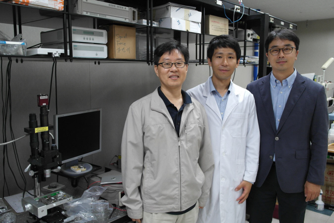
 Graduate Student at KAIST Awarded Best Prize at the 9th Inside Edge
Sun-Jin Choi, a Ph. D. candidate in the Department of Materials Science and Engineering at KAIST, under the guidance of Professor Il-Doo Kim, won the best prize at the 9th Inside Edge Contest hosted by Samsung Electro-Mechanics.
Choi was awarded prize money totaling fifteen million won at the award ceremony held on November 22 at the Mirae Hall at the headquarters of Samsung Electro-Mechanics in Suwon.
Choi’s research, titled “Exhaled Breath Sensor Arrays for the Non-invasive and Real-time Diagnosis of Diabetes by Detection of Acetone,” was recognized for its creativity and uniqueness.The Inside Edge is an international thesis competition which was started in 2005 to encourage and support creative research and potential technological development among young scientists and engineers.
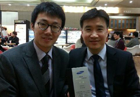
Sun-Jin Choi (left) and Professor Il-Doo Kim (right).
2013.12.11 View 11581
Graduate Student at KAIST Awarded Best Prize at the 9th Inside Edge
Sun-Jin Choi, a Ph. D. candidate in the Department of Materials Science and Engineering at KAIST, under the guidance of Professor Il-Doo Kim, won the best prize at the 9th Inside Edge Contest hosted by Samsung Electro-Mechanics.
Choi was awarded prize money totaling fifteen million won at the award ceremony held on November 22 at the Mirae Hall at the headquarters of Samsung Electro-Mechanics in Suwon.
Choi’s research, titled “Exhaled Breath Sensor Arrays for the Non-invasive and Real-time Diagnosis of Diabetes by Detection of Acetone,” was recognized for its creativity and uniqueness.The Inside Edge is an international thesis competition which was started in 2005 to encourage and support creative research and potential technological development among young scientists and engineers.
Sun-Jin Choi (left) and Professor Il-Doo Kim (right).
2013.12.11 View 11581 -
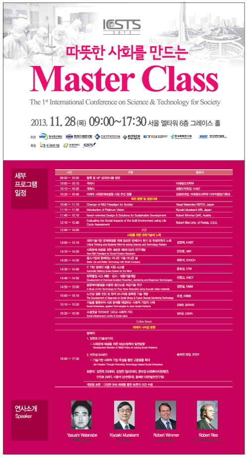 First International Conference on Science and Technology for Society
KAIST co-organized the 2013 International Conference on Science and Technology for Society which was held on November 28 at the Grace Hall in Seoul EL-Tower. More than 300 people, including members of the Global Social Technology Advisory Board, domestic social technology experts, private companies, government officials, private citizens, and students joined the conference to discuss the roles and responsibilities of science and technology for society.
R&D policies and technologies for solving social issues were introduced, and discussions were held on desirable directions for technological development.
The first speaker, Yasushi Watanabe, Director of RISTEX (Research Institute of Science and Technology for Society) in Japan, introduced the importance of science and technology for society under the title “Change of R&D Paradigm for Society.”
Robert Wimmer, GrAT (Center for Appropriate Technology), Vienna University of Technology in Austria, presented “Need-oriented Design & Solutions for Development.” Kiyoaki Murakami, MRI, Japan, presented “Introduction of Platinum Vision” and Robert Ries, University of Florida, U.S.A., presented “Evaluating the Social Impacts of the Built Environment Using Life Cycle Assessment.”
Case studies on social enterprises and presentations on R&D for solving social problems were introduced by ICISTS (International Conference for the Integration of Science, Technology and Society), which is a student group at KAIST, National Research Foundation of Korea (NRF), Korea Institute of Machinery and Materials (KIMM), Korea Research Institute of Bioscience and Biotechnology (KRIBB), Korea Institute of Industrial Technology (KITECH), Electronics and Telecommunication Research Institute (ETRI), and Korea Research Institute of Chemical Technology (KRICT).The conference was hosted by the Ministry of Science, ICT, and Future Planning and co-organized by NRF, KIMM, KRIBB, KITECH, ETRI and KRICT.
2013.12.11 View 14428
First International Conference on Science and Technology for Society
KAIST co-organized the 2013 International Conference on Science and Technology for Society which was held on November 28 at the Grace Hall in Seoul EL-Tower. More than 300 people, including members of the Global Social Technology Advisory Board, domestic social technology experts, private companies, government officials, private citizens, and students joined the conference to discuss the roles and responsibilities of science and technology for society.
R&D policies and technologies for solving social issues were introduced, and discussions were held on desirable directions for technological development.
The first speaker, Yasushi Watanabe, Director of RISTEX (Research Institute of Science and Technology for Society) in Japan, introduced the importance of science and technology for society under the title “Change of R&D Paradigm for Society.”
Robert Wimmer, GrAT (Center for Appropriate Technology), Vienna University of Technology in Austria, presented “Need-oriented Design & Solutions for Development.” Kiyoaki Murakami, MRI, Japan, presented “Introduction of Platinum Vision” and Robert Ries, University of Florida, U.S.A., presented “Evaluating the Social Impacts of the Built Environment Using Life Cycle Assessment.”
Case studies on social enterprises and presentations on R&D for solving social problems were introduced by ICISTS (International Conference for the Integration of Science, Technology and Society), which is a student group at KAIST, National Research Foundation of Korea (NRF), Korea Institute of Machinery and Materials (KIMM), Korea Research Institute of Bioscience and Biotechnology (KRIBB), Korea Institute of Industrial Technology (KITECH), Electronics and Telecommunication Research Institute (ETRI), and Korea Research Institute of Chemical Technology (KRICT).The conference was hosted by the Ministry of Science, ICT, and Future Planning and co-organized by NRF, KIMM, KRIBB, KITECH, ETRI and KRICT.
2013.12.11 View 14428 -
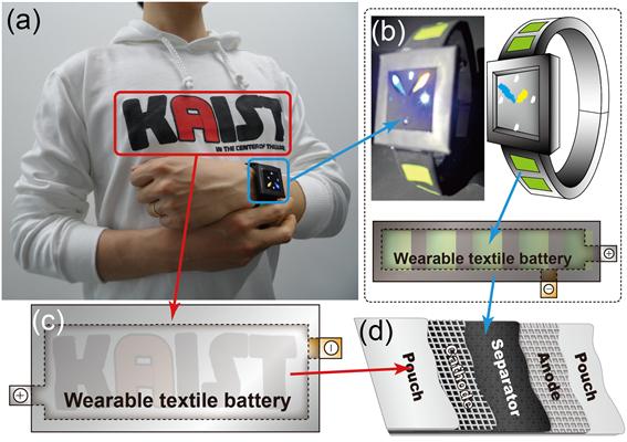 Technology Developed for Flexible, Foldable & Rechargeable Battery
Flexible, Foldable & Rechargeable Battery
The research group of professors Jang-Wook Choi & Jung-Yong Lee from the Graduate School of EEWS and Taek-Soo Kim from the Department of Mechanical Engineering at KAIST has developed technology for flexible and foldable batteries which are rechargeable using solar energy. The research result was published in the online issue of Nano Letters on November 5.
Trial versions of flexible and wearable electronics are being developed and introduced in the market such as Galaxy Gear, Apple’s i-Watch, and Google Glass. Research is being conducted to make the batteries softer and more wearable and to compete in the fast-growing market for flexible electronics.
This new technology is expected to be applied to the development of wearable computers as well as winter outdoor clothing since it is flexible and light. The research group expects that the new technology can be applied to current battery production lines without additional investment.
Professor Choi said, “It can be used as a core-source technology in the rechargeable battery industry in the future. Various wearable mobile electronic products can be developed through cooperation and collaboration within the industry.”
2013.11.21 View 14072
Technology Developed for Flexible, Foldable & Rechargeable Battery
Flexible, Foldable & Rechargeable Battery
The research group of professors Jang-Wook Choi & Jung-Yong Lee from the Graduate School of EEWS and Taek-Soo Kim from the Department of Mechanical Engineering at KAIST has developed technology for flexible and foldable batteries which are rechargeable using solar energy. The research result was published in the online issue of Nano Letters on November 5.
Trial versions of flexible and wearable electronics are being developed and introduced in the market such as Galaxy Gear, Apple’s i-Watch, and Google Glass. Research is being conducted to make the batteries softer and more wearable and to compete in the fast-growing market for flexible electronics.
This new technology is expected to be applied to the development of wearable computers as well as winter outdoor clothing since it is flexible and light. The research group expects that the new technology can be applied to current battery production lines without additional investment.
Professor Choi said, “It can be used as a core-source technology in the rechargeable battery industry in the future. Various wearable mobile electronic products can be developed through cooperation and collaboration within the industry.”
2013.11.21 View 14072 -
 Observation of a water strider led to a new method of measuring properties of Nano films
Even the mechanical properties of Nano films of a few nanometers thick can be measured
Posted online Nature Communications on the 3rd of October
The joint research team of KAIST’s Department of Mechanical Engineering’s Professor Taek-Soo Kim and Doctor Seung-Min Hyun of the Nano mechanics laboratory of Korea Institute of Machinery and Materials has developed a new method to evaluate mechanical properties of Nano films using the characteristics of water surfaces.
The research findings have been posted on the online edition of Nature Communications on the 3rd of October. The technology can obtain accurate results by directly measuring the mechanical properties such as the strength and elasticity of Nano films. Academia and the industry expect the simplicity of the technology to present a new paradigm in the evaluation of mechanical properties of Nano films.
Evaluation of the mechanical properties of Nano films is essential not only in predicting the reliability of semiconductors and displays, but also in finding new phenomena in the Nano world. However, mechanical strength was difficult to test since the test demands the falling of objects to the ground to measure their strength, and nano films can easily break in the process.
The research team observed insects such as water striders freely floating on the surface of the water. The team used the properties of water, large surface tension and low viscosity, to float a 55 nanometers (nm) gold Nano film to successfully measure its mechanical properties without damaging it. The technology could be used to measure the mechanical properties of not only various types of Nano films but also films only a few nm thick.
Professor Taek-Soo Kim said, “We effectively performed an evaluation of the mechanical characteristics of Nano films, which was difficult in the past, by developing a new strength test using the properties of water.” He continued to say, “The team plans to discover the mechanical properties of 2D Nano films such as graphene that could not have been measured with the existing strength test methods.”
The research by KAIST’s Department of Mechanical Engineering’s graduate student Jae-Han Kim (lead author) under the supervision of Professor Taek-Soo Kim and Doctor Seung-Min Hyun of Korea Institute of Machinery and Materials was sponsored by the National Research Foundation of Korea.
Evaluation process of mechanical properties of Nano films by using the characteristics of water surfaces
Dr Seung-Min Hyun, Jae-Han Kim, and Professor Taek-Soo Kim from left to right
2013.11.11 View 10392
Observation of a water strider led to a new method of measuring properties of Nano films
Even the mechanical properties of Nano films of a few nanometers thick can be measured
Posted online Nature Communications on the 3rd of October
The joint research team of KAIST’s Department of Mechanical Engineering’s Professor Taek-Soo Kim and Doctor Seung-Min Hyun of the Nano mechanics laboratory of Korea Institute of Machinery and Materials has developed a new method to evaluate mechanical properties of Nano films using the characteristics of water surfaces.
The research findings have been posted on the online edition of Nature Communications on the 3rd of October. The technology can obtain accurate results by directly measuring the mechanical properties such as the strength and elasticity of Nano films. Academia and the industry expect the simplicity of the technology to present a new paradigm in the evaluation of mechanical properties of Nano films.
Evaluation of the mechanical properties of Nano films is essential not only in predicting the reliability of semiconductors and displays, but also in finding new phenomena in the Nano world. However, mechanical strength was difficult to test since the test demands the falling of objects to the ground to measure their strength, and nano films can easily break in the process.
The research team observed insects such as water striders freely floating on the surface of the water. The team used the properties of water, large surface tension and low viscosity, to float a 55 nanometers (nm) gold Nano film to successfully measure its mechanical properties without damaging it. The technology could be used to measure the mechanical properties of not only various types of Nano films but also films only a few nm thick.
Professor Taek-Soo Kim said, “We effectively performed an evaluation of the mechanical characteristics of Nano films, which was difficult in the past, by developing a new strength test using the properties of water.” He continued to say, “The team plans to discover the mechanical properties of 2D Nano films such as graphene that could not have been measured with the existing strength test methods.”
The research by KAIST’s Department of Mechanical Engineering’s graduate student Jae-Han Kim (lead author) under the supervision of Professor Taek-Soo Kim and Doctor Seung-Min Hyun of Korea Institute of Machinery and Materials was sponsored by the National Research Foundation of Korea.
Evaluation process of mechanical properties of Nano films by using the characteristics of water surfaces
Dr Seung-Min Hyun, Jae-Han Kim, and Professor Taek-Soo Kim from left to right
2013.11.11 View 10392 -
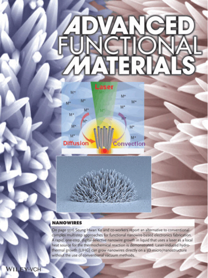 Ultra High Speed Nanomaterial Synthesis Process Developed Using Laser
Dr. Jun-Yeop, Yeo and the research team led by Professor Seung-Hwan, Ko (both of the Department of Mechanical Engineering) successfully developed a process enabling the location-determinable, ultra high speed synthesis of nanomaterials using concentrated laser beams.
The result of the research effort was published as the frontispiece in the July 9th issue of Advanced Functional Materials, a world renowned material science and engineering academic journal.
Application of the technology reduced the time needed to process nanomaterial synthesis from a few hours to a mere five minutes. In addition, unlike conventional nanomaterial synthesis processes, it is simple enough to enable mass production and commercialization.
Conventional processes require the high temperatures of 900~1,000 °C and the use of toxic or explosive vapors. Complex processes such as separation after synthesis and patterning are needed for application in electronic devices. The multi-step, expensive, environmentally unfriendly characteristics of nanomaterial synthesis served as road blocks to its mass production and commercialization.
Exposing the precursor to concentrated continuous laser beam (green wavelength) resulted in the synthesis of nanowires in the desired location; the first instance in the world to accomplish this feat. The technology, according to the research team, makes possible the production, integration and patterning of nanomaterials using a single process. Applicable to various surfaces and substrates, nanowires have been successfully synthesized on flexible plastic substrates and controlled patterning on the surface of 3-dimensional structures.
Dr. Yeo commented that the research effort has “yielded the creation of a nanomaterial synthesis process capable of synthesis, integration, pattern, and material production using light energy” and has “reduced the synthesis process time of nanomaterial to one tenths of the conventional process.” Dr. Yeo continues to devise steps to commercialize the new multifunctional electronic material and methods for mass production.
The research effort, led by Dr. Yeo and Professor Ko, received contribution from Professor Hyung-Jin Sung (KAIST Department of Mechanical Engineering), Seok-Joon Hong, a Ph.D. candidate, Hyun-Wook Kang, also a Ph.D. candidate, Professor Costas Grigoropoulos of UC Berkeley, and Dr. Dae Ho Lee. In addition, the team received support from the National Research Foundation, Ministry of Knowledge Economy, Global Frontier Program, and KAIST EEWS.
Picture I: Synthesized nanomaterials produced at a desirable location by laser beams
Picture 2: Synthesized nanomaterials built on the 3D structure by using the developed technology
Picture 3: Functional electric circuit made with synthesized nanomaterials
Picture 4: Cover page of July 9th issue of Advanced Functional Materials
2013.08.23 View 12037
Ultra High Speed Nanomaterial Synthesis Process Developed Using Laser
Dr. Jun-Yeop, Yeo and the research team led by Professor Seung-Hwan, Ko (both of the Department of Mechanical Engineering) successfully developed a process enabling the location-determinable, ultra high speed synthesis of nanomaterials using concentrated laser beams.
The result of the research effort was published as the frontispiece in the July 9th issue of Advanced Functional Materials, a world renowned material science and engineering academic journal.
Application of the technology reduced the time needed to process nanomaterial synthesis from a few hours to a mere five minutes. In addition, unlike conventional nanomaterial synthesis processes, it is simple enough to enable mass production and commercialization.
Conventional processes require the high temperatures of 900~1,000 °C and the use of toxic or explosive vapors. Complex processes such as separation after synthesis and patterning are needed for application in electronic devices. The multi-step, expensive, environmentally unfriendly characteristics of nanomaterial synthesis served as road blocks to its mass production and commercialization.
Exposing the precursor to concentrated continuous laser beam (green wavelength) resulted in the synthesis of nanowires in the desired location; the first instance in the world to accomplish this feat. The technology, according to the research team, makes possible the production, integration and patterning of nanomaterials using a single process. Applicable to various surfaces and substrates, nanowires have been successfully synthesized on flexible plastic substrates and controlled patterning on the surface of 3-dimensional structures.
Dr. Yeo commented that the research effort has “yielded the creation of a nanomaterial synthesis process capable of synthesis, integration, pattern, and material production using light energy” and has “reduced the synthesis process time of nanomaterial to one tenths of the conventional process.” Dr. Yeo continues to devise steps to commercialize the new multifunctional electronic material and methods for mass production.
The research effort, led by Dr. Yeo and Professor Ko, received contribution from Professor Hyung-Jin Sung (KAIST Department of Mechanical Engineering), Seok-Joon Hong, a Ph.D. candidate, Hyun-Wook Kang, also a Ph.D. candidate, Professor Costas Grigoropoulos of UC Berkeley, and Dr. Dae Ho Lee. In addition, the team received support from the National Research Foundation, Ministry of Knowledge Economy, Global Frontier Program, and KAIST EEWS.
Picture I: Synthesized nanomaterials produced at a desirable location by laser beams
Picture 2: Synthesized nanomaterials built on the 3D structure by using the developed technology
Picture 3: Functional electric circuit made with synthesized nanomaterials
Picture 4: Cover page of July 9th issue of Advanced Functional Materials
2013.08.23 View 12037 -
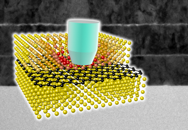 Ultra-High Strength Metamaterial Developed Using Graphene
New metamaterial has been developed, exhibiting hundreds of times greater strength than pure metals.
Professor Seung Min, Han and Yoo Sung, Jeong (Graduate School of Energy, Environment, Water, and Sustainability (EEWS)) and Professor Seok Woo, Jeon (Department of Material Science and Engineering) have developed a composite nanomaterial. The nanomaterial consists of graphene inserted in copper and nickel and exhibits strengths 500 times and 180 times, respectively, greater than that of pure metals. The result of the research was published on the July 2nd online edition in Nature Communications journal.
Graphene displays strengths 200 times greater than that of steel, is stretchable, and is flexible. The U.S. Army Armaments Research, Development and Engineering Center developed a graphene-metal nanomaterial but failed to drastically improve the strength of the material.
To maximize the strength increased by the addition of graphene, the KAIST research team created a layered structure of metal and graphene. Using CVD (Chemical Vapor Deposition), the team grew a single layer of graphene on a metal deposited substrate and then deposited another metal layer. They repeated this process to produce a metal-graphene multilayer composite material, utilizing a single layer of graphene. Micro-compression tests within Transmission Electronic Microscope and Molecular Dynamics simulations effectively showed the strength enhancing effect and the dislocation movement in grain boundaries of graphene on an atomic level.
The mechanical characteristics of the graphene layer within the metal-graphene composite material successfully blocked the dislocations and cracks from external damage from traveling inwards. Therefore the composite material displayed strength beyond conventional metal-metal multilayer materials. The copper-graphene multilayer material with an interplanar distance of 70nm exhibited 500 times greater (1.5GPa) strength than pure copper. Nickel-graphene multilayer material with an interplanar distance of 100nm showed 180 times greater (4.0GPa) strength than pure nickel.
It was found that there is a clear relationship between the interplanar distance and the strength of the multilayer material. A smaller interplanar distance made the dislocation movement more difficult and therefore increased the strength of the material. Professor Han, who led the research, commented, “the result is astounding as 0.00004% in weight of graphene increased the strength of the materials by hundreds of times” and “improvements based on this success, especially mass production with roll-to-roll process or metal sintering process in the production of ultra-high strength, lightweight parts for automobile and spacecraft, may become possible.” In addition, Professor Han mentioned that “the new material can be applied to coating materials for nuclear reactor construction or other structural materials requiring high reliability.”
The research project received support from National Research Foundation, Global Frontier Program, KAIST EEWS-KINC Program and KISTI Supercomputer and was a collaborative effort with KISTI (Korea Institute of Science and Technology Information), KBSI (Korea Basic Science Institute), Stanford University, and Columbia University.
A schematic diagram shows the structure of metal-graphene multi-layers. The metal-graphene multi-layered composite materials, containing a single-layered graphene, block the dislocation movement of graphene layers, resulting in a greater strength in the materials.
2013.08.23 View 19494
Ultra-High Strength Metamaterial Developed Using Graphene
New metamaterial has been developed, exhibiting hundreds of times greater strength than pure metals.
Professor Seung Min, Han and Yoo Sung, Jeong (Graduate School of Energy, Environment, Water, and Sustainability (EEWS)) and Professor Seok Woo, Jeon (Department of Material Science and Engineering) have developed a composite nanomaterial. The nanomaterial consists of graphene inserted in copper and nickel and exhibits strengths 500 times and 180 times, respectively, greater than that of pure metals. The result of the research was published on the July 2nd online edition in Nature Communications journal.
Graphene displays strengths 200 times greater than that of steel, is stretchable, and is flexible. The U.S. Army Armaments Research, Development and Engineering Center developed a graphene-metal nanomaterial but failed to drastically improve the strength of the material.
To maximize the strength increased by the addition of graphene, the KAIST research team created a layered structure of metal and graphene. Using CVD (Chemical Vapor Deposition), the team grew a single layer of graphene on a metal deposited substrate and then deposited another metal layer. They repeated this process to produce a metal-graphene multilayer composite material, utilizing a single layer of graphene. Micro-compression tests within Transmission Electronic Microscope and Molecular Dynamics simulations effectively showed the strength enhancing effect and the dislocation movement in grain boundaries of graphene on an atomic level.
The mechanical characteristics of the graphene layer within the metal-graphene composite material successfully blocked the dislocations and cracks from external damage from traveling inwards. Therefore the composite material displayed strength beyond conventional metal-metal multilayer materials. The copper-graphene multilayer material with an interplanar distance of 70nm exhibited 500 times greater (1.5GPa) strength than pure copper. Nickel-graphene multilayer material with an interplanar distance of 100nm showed 180 times greater (4.0GPa) strength than pure nickel.
It was found that there is a clear relationship between the interplanar distance and the strength of the multilayer material. A smaller interplanar distance made the dislocation movement more difficult and therefore increased the strength of the material. Professor Han, who led the research, commented, “the result is astounding as 0.00004% in weight of graphene increased the strength of the materials by hundreds of times” and “improvements based on this success, especially mass production with roll-to-roll process or metal sintering process in the production of ultra-high strength, lightweight parts for automobile and spacecraft, may become possible.” In addition, Professor Han mentioned that “the new material can be applied to coating materials for nuclear reactor construction or other structural materials requiring high reliability.”
The research project received support from National Research Foundation, Global Frontier Program, KAIST EEWS-KINC Program and KISTI Supercomputer and was a collaborative effort with KISTI (Korea Institute of Science and Technology Information), KBSI (Korea Basic Science Institute), Stanford University, and Columbia University.
A schematic diagram shows the structure of metal-graphene multi-layers. The metal-graphene multi-layered composite materials, containing a single-layered graphene, block the dislocation movement of graphene layers, resulting in a greater strength in the materials.
2013.08.23 View 19494 -
 High Speed Nanomanufacturing Process Developed using Laser
Dr. Yeo Jun Yeop from KAIST’s Department of Mechanical Engineering, in a joint research project with Prof. Seung Hwan Ko, has developed a technology that speeds up the nanomanufacturing process by using lasers. Their research is published in the frontispiece of Advanced Functional Materials (July 9th issue).
Fig. The frontispiece of Advanced Functional Materials(July 9th issue)
The research group put a nanomaterial precursor on the board, illuminated it with a continuous-wave laser in the green wavelength range, and succeeded in synthesizing a nanowire at the point they wanted for the first time in the world.
Currently nanomaterials are difficult to mass produce and commercialize due to their complex and costly manufacturing processes which also use toxic gases. However, their new technology simplified the process and so reduced the manufacturing time from some hours to five minutes (1/10th times reduced).
Furthermore, this technology will apply regardless of the type of the board. Such nanometerials can be synthesized at any point on a flexible plastic board or even in three dimensional structures by illuminating them with a simple laser. Academics and industries expect mass production and commercialization of nanomaterials in near future.
Dr. Yeo said he intends to research further to promote early commercialization of multifunctional electronic devices by combining various nanomaterials
This research is sponsored by the National Research Foundation of Korea, the Ministry of Trade, Industry and Energy and KAIST EEWS
Fig. A nanomaterial synthesized after illuminated by lasers
Fig. A nanomaterial synthesized on a three dimensional structure using the developed technology
Fig. Functional electron device manufactured by using the synthesized nanomaterials
2013.08.02 View 10676
High Speed Nanomanufacturing Process Developed using Laser
Dr. Yeo Jun Yeop from KAIST’s Department of Mechanical Engineering, in a joint research project with Prof. Seung Hwan Ko, has developed a technology that speeds up the nanomanufacturing process by using lasers. Their research is published in the frontispiece of Advanced Functional Materials (July 9th issue).
Fig. The frontispiece of Advanced Functional Materials(July 9th issue)
The research group put a nanomaterial precursor on the board, illuminated it with a continuous-wave laser in the green wavelength range, and succeeded in synthesizing a nanowire at the point they wanted for the first time in the world.
Currently nanomaterials are difficult to mass produce and commercialize due to their complex and costly manufacturing processes which also use toxic gases. However, their new technology simplified the process and so reduced the manufacturing time from some hours to five minutes (1/10th times reduced).
Furthermore, this technology will apply regardless of the type of the board. Such nanometerials can be synthesized at any point on a flexible plastic board or even in three dimensional structures by illuminating them with a simple laser. Academics and industries expect mass production and commercialization of nanomaterials in near future.
Dr. Yeo said he intends to research further to promote early commercialization of multifunctional electronic devices by combining various nanomaterials
This research is sponsored by the National Research Foundation of Korea, the Ministry of Trade, Industry and Energy and KAIST EEWS
Fig. A nanomaterial synthesized after illuminated by lasers
Fig. A nanomaterial synthesized on a three dimensional structure using the developed technology
Fig. Functional electron device manufactured by using the synthesized nanomaterials
2013.08.02 View 10676 -
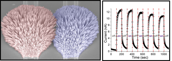
 Nanofiber sensor detects diabetes or lung cancer faster and easier
Metal-oxide nanofiber based chemiresistive gas sensors offer greater usability for portable real-time breath tests that can be available on smart phones or tablet PCs in the near future.
Daejeon, Republic of Korea, June 11, 2013 -- Today"s technological innovation enables smartphone users to diagnose serious diseases such as diabetes or lung cancer quickly and effectively by simply breathing into a small gadget, a nanofiber breathing sensor, mounted on the phones.
Il-Doo Kim, Associate Professor of Materials Science and Engineering Department at the Korea Advanced Institute of Science and Technology (KAIST), and his research team have recently published a cover paper entitled "Thin-Wall Assembled SnO2 Fibers Functionalized by Catalytic Pt Nanoparticles and their Superior Exhaled Breath-Sensing Properties for the Diagnosis of Diabetes," in an academic journal, Advanced Functional Materials (May 20th issue), on the development of a highly sensitive exhaled breath sensor by using hierarchical SnO2 fibers that are assembled from wrinkled thin SnO2 nanotubes.
In the paper, the research team presented a morphological evolution of SnO2 fibers, called micro phase-separations, which takes place between polymers and other dissolved solutes when varying the flow rate of an electrospinning solution feed and applying a subsequent heat treatment afterward.
The morphological change results in nanofibers that are shaped like an open cylinder inside which thin-film SnO2 nanotubes are layered and then rolled up. A number of elongated pores ranging from 10 nanometers (nm) to 500 nm in length along the fiber direction were formed on the surface of the SnO2 fibers, allowing exhaled gas molecules to easily permeate the fibers. The inner and outer wall of SnO2 tubes is evenly coated with catalytic platinum (Pt) nanoparticles. According to the research team, highly porous SnO2 fibers, synthesized by eletrospinning at a high flow rate, showed five-fold higher acetone responses than that of the dense SnO2 nanofibers created under a low flow rate. The catalytic Pt coating shortened the fibers" gas response time dramatically as well.
The breath analysis for diabetes is largely based on an acetone breath test because acetone is one of the specific volatile organic compounds (VOC) produced in the human body to signal the onset of particular diseases. In other words, they are biomarkers to predict certain diseases such as acetone for diabetes, toluene for lung cancer, and ammonia for kidney malfunction. Breath analysis for medical evaluation has attracted much attention because it is less intrusive than conventional medical examination, as well as fast and convenient, and environmentally friendly, leaving almost no biohazard wastes.
Various gas-sensing techniques have been adopted to analyze VOCs including gas chromatography-mass spectroscopy (GC-MS), but these techniques are difficult to incorporate into portable real-time gas sensors because the testing equipment is bulky and expensive, and their operation is more complex. Metal-oxide based chemiresistive gas sensors, however, offer greater usability for portable real-time breath sensors.
Il-Doo Kim said, "Catalyst-loaded metal oxide nanofibers synthesized by electrospinning have a great potential for future exhaled breath sensor applications. From our research, we obtained the results that Pt-coated SnO2 fibers are able to identify promptly and accurately acetone or toluene even at very low concentration less than 100 parts per billion (ppb)."
The exhaled acetone level of diabetes patients exceeds 1.8 parts per million (ppm), which is two to six-fold higher than that (0.3-0.9 ppm) of healthy people. Therefore, a highly sensitive detection that responds to acetone below 1 ppm, in the presence of other exhaled gases as well as under the humid environment of human breath, is important for an accurate diagnosis of diabetes. In addition, Professor Kim said, "a trace concentration of toluene (30 ppb) in exhaled breath is regarded to be a distinctive early symptom of lung cancer, which we were able to detect with our prototype breath tester."
The research team has now been developing an array of breathing sensors using various catalysts and a number of semiconducting metal oxide fibers, which will offer patients a real-time easy diagnosis of diseases.
###
Youtube Link: http://www.youtube.com/watch?v=t_Hr11dRryg
For further inquires:
Il-Doo Kim, Professor of Materials Science and Engineering, KAIST
Advanced Nanomaterials and Energy Laboratory
Tel: +82-42-350-3329
Email: idkim@kaist.ac.kr
Clockwise from left to right: left upper shows a magnified SEM image of a broken thin-wall assembled SnO2 fiber. Left below is an array of breath sensors (Inset is an actual size of a breath sensor). The right is the cover of Advanced Functional Materials (May 20th issue) in which a research paper on the development of a highly sensitive exhaled breath sensor by using SnO2 fibers is published.
This is the microstructural evolution of SnO2 nanofibers as a function of flow rate during electrospinning.
2013.06.20 View 15842
Nanofiber sensor detects diabetes or lung cancer faster and easier
Metal-oxide nanofiber based chemiresistive gas sensors offer greater usability for portable real-time breath tests that can be available on smart phones or tablet PCs in the near future.
Daejeon, Republic of Korea, June 11, 2013 -- Today"s technological innovation enables smartphone users to diagnose serious diseases such as diabetes or lung cancer quickly and effectively by simply breathing into a small gadget, a nanofiber breathing sensor, mounted on the phones.
Il-Doo Kim, Associate Professor of Materials Science and Engineering Department at the Korea Advanced Institute of Science and Technology (KAIST), and his research team have recently published a cover paper entitled "Thin-Wall Assembled SnO2 Fibers Functionalized by Catalytic Pt Nanoparticles and their Superior Exhaled Breath-Sensing Properties for the Diagnosis of Diabetes," in an academic journal, Advanced Functional Materials (May 20th issue), on the development of a highly sensitive exhaled breath sensor by using hierarchical SnO2 fibers that are assembled from wrinkled thin SnO2 nanotubes.
In the paper, the research team presented a morphological evolution of SnO2 fibers, called micro phase-separations, which takes place between polymers and other dissolved solutes when varying the flow rate of an electrospinning solution feed and applying a subsequent heat treatment afterward.
The morphological change results in nanofibers that are shaped like an open cylinder inside which thin-film SnO2 nanotubes are layered and then rolled up. A number of elongated pores ranging from 10 nanometers (nm) to 500 nm in length along the fiber direction were formed on the surface of the SnO2 fibers, allowing exhaled gas molecules to easily permeate the fibers. The inner and outer wall of SnO2 tubes is evenly coated with catalytic platinum (Pt) nanoparticles. According to the research team, highly porous SnO2 fibers, synthesized by eletrospinning at a high flow rate, showed five-fold higher acetone responses than that of the dense SnO2 nanofibers created under a low flow rate. The catalytic Pt coating shortened the fibers" gas response time dramatically as well.
The breath analysis for diabetes is largely based on an acetone breath test because acetone is one of the specific volatile organic compounds (VOC) produced in the human body to signal the onset of particular diseases. In other words, they are biomarkers to predict certain diseases such as acetone for diabetes, toluene for lung cancer, and ammonia for kidney malfunction. Breath analysis for medical evaluation has attracted much attention because it is less intrusive than conventional medical examination, as well as fast and convenient, and environmentally friendly, leaving almost no biohazard wastes.
Various gas-sensing techniques have been adopted to analyze VOCs including gas chromatography-mass spectroscopy (GC-MS), but these techniques are difficult to incorporate into portable real-time gas sensors because the testing equipment is bulky and expensive, and their operation is more complex. Metal-oxide based chemiresistive gas sensors, however, offer greater usability for portable real-time breath sensors.
Il-Doo Kim said, "Catalyst-loaded metal oxide nanofibers synthesized by electrospinning have a great potential for future exhaled breath sensor applications. From our research, we obtained the results that Pt-coated SnO2 fibers are able to identify promptly and accurately acetone or toluene even at very low concentration less than 100 parts per billion (ppb)."
The exhaled acetone level of diabetes patients exceeds 1.8 parts per million (ppm), which is two to six-fold higher than that (0.3-0.9 ppm) of healthy people. Therefore, a highly sensitive detection that responds to acetone below 1 ppm, in the presence of other exhaled gases as well as under the humid environment of human breath, is important for an accurate diagnosis of diabetes. In addition, Professor Kim said, "a trace concentration of toluene (30 ppb) in exhaled breath is regarded to be a distinctive early symptom of lung cancer, which we were able to detect with our prototype breath tester."
The research team has now been developing an array of breathing sensors using various catalysts and a number of semiconducting metal oxide fibers, which will offer patients a real-time easy diagnosis of diseases.
###
Youtube Link: http://www.youtube.com/watch?v=t_Hr11dRryg
For further inquires:
Il-Doo Kim, Professor of Materials Science and Engineering, KAIST
Advanced Nanomaterials and Energy Laboratory
Tel: +82-42-350-3329
Email: idkim@kaist.ac.kr
Clockwise from left to right: left upper shows a magnified SEM image of a broken thin-wall assembled SnO2 fiber. Left below is an array of breath sensors (Inset is an actual size of a breath sensor). The right is the cover of Advanced Functional Materials (May 20th issue) in which a research paper on the development of a highly sensitive exhaled breath sensor by using SnO2 fibers is published.
This is the microstructural evolution of SnO2 nanofibers as a function of flow rate during electrospinning.
2013.06.20 View 15842 -
 New Technology Will Enable the Commercialization of Plasmon Displays
-- Enhancements in the penetration ratios of color filters are expected by applying nano-surface plasmon effects. --
-- Color filter technology will be applicable to large-area OLED and LCD. --
The fabrication technology to commercialize display color filters using plasmon effects has been discovered.
A joint research team headed by Professor Kyung Cheol Choi from the Department of Electrical Engineering of the Korea Advanced Institute for Science and Technology and Prof. Byeong-Kwon Ju from the School of Electrical Engineering of Korea University has developed the technology to design and produce a display color filter by applying nano-surface plasmon effects.
Color filters are core components used to express colors in CMOS image sensors found in LCD/OLED displays or digital cameras. The current color filters have penetration ratios of 20~30%, but the objective of the joint research team is to raise this penetration ratio by over 40% to facilitate the mass production of energy-efficient plasmonic displays.
Currently available plasmonic color filters are limited to applications on micrometer scales. However, outcomes of the newest research extend the size of the applications up to 2.5 cm by using laser interference lithography. The academic and industrial sectors agree that it is now possible to mass-produce displays using plasmonic color filters.
The researchers built a nanohole array to large scale by using laser interference lithography, a technology that forms nanostructures with laser light interferences. They also suggested a new manufacturing process that can optimize the features of color filters while compensating for defects arising from the fabrication stages.
The new manufacturing process of applying laser interference lithography is expected to overcome the shortcomings of traditional color filters by simplifying production and, enabling them to be produced at lower costs.
“There were limitations to industrial applications of plasmon effect due to production costs, time, and yields,” explained Yun Seon Do, a Ph. D. candidate in the Department of Electrical Engineering of KAIST. “The new technology can reduce fabrication time and cost to the extent that it would be advisable to replace dye-based and pigment-based color filter technology."
“This research can be applied to large-scale displays, such as TV screens, by using laser-interference lithography,” said Jung-Ho Park, a Ph. D. candidate in the School of Electrical Engineering of Korea University. “The research outcome is expected to be widely applied in advanced nano-manufacturing processes as it does not restrict the types of circuit boards."
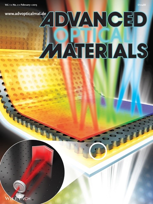
The research outcome, led by doctoral candidates Do and Park, appeared on the front cover of the second issue of Advanced Optical Materials, a highly regarded academic journal in the field of nanotechnologies, and the team has applied for six related patents.
2013.03.13 View 10588
New Technology Will Enable the Commercialization of Plasmon Displays
-- Enhancements in the penetration ratios of color filters are expected by applying nano-surface plasmon effects. --
-- Color filter technology will be applicable to large-area OLED and LCD. --
The fabrication technology to commercialize display color filters using plasmon effects has been discovered.
A joint research team headed by Professor Kyung Cheol Choi from the Department of Electrical Engineering of the Korea Advanced Institute for Science and Technology and Prof. Byeong-Kwon Ju from the School of Electrical Engineering of Korea University has developed the technology to design and produce a display color filter by applying nano-surface plasmon effects.
Color filters are core components used to express colors in CMOS image sensors found in LCD/OLED displays or digital cameras. The current color filters have penetration ratios of 20~30%, but the objective of the joint research team is to raise this penetration ratio by over 40% to facilitate the mass production of energy-efficient plasmonic displays.
Currently available plasmonic color filters are limited to applications on micrometer scales. However, outcomes of the newest research extend the size of the applications up to 2.5 cm by using laser interference lithography. The academic and industrial sectors agree that it is now possible to mass-produce displays using plasmonic color filters.
The researchers built a nanohole array to large scale by using laser interference lithography, a technology that forms nanostructures with laser light interferences. They also suggested a new manufacturing process that can optimize the features of color filters while compensating for defects arising from the fabrication stages.
The new manufacturing process of applying laser interference lithography is expected to overcome the shortcomings of traditional color filters by simplifying production and, enabling them to be produced at lower costs.
“There were limitations to industrial applications of plasmon effect due to production costs, time, and yields,” explained Yun Seon Do, a Ph. D. candidate in the Department of Electrical Engineering of KAIST. “The new technology can reduce fabrication time and cost to the extent that it would be advisable to replace dye-based and pigment-based color filter technology."
“This research can be applied to large-scale displays, such as TV screens, by using laser-interference lithography,” said Jung-Ho Park, a Ph. D. candidate in the School of Electrical Engineering of Korea University. “The research outcome is expected to be widely applied in advanced nano-manufacturing processes as it does not restrict the types of circuit boards."
The research outcome, led by doctoral candidates Do and Park, appeared on the front cover of the second issue of Advanced Optical Materials, a highly regarded academic journal in the field of nanotechnologies, and the team has applied for six related patents.
2013.03.13 View 10588 -
 The control of light at the nano-level
Professor Min Bumki
Professor Min Bumki’s research team from the Department of Mechanical Engineering at KAIST have successfully gained control of the transmittance of light in optical devices using graphene* and artificial 2-dimensional metamaterials**.
* Graphene : a thin membrane composed of pure carbon, with atoms arranged in a regular hexagonal pattern
** Metamaterials : artificial materials engineered to have properties that may not be found in nature
The research results were published in the recent online edition (September 30th) of Nature Materials, a sister journal of the world renowned Nature journal, under the title ‘Terahertz waves with gate-controlled active graphene metamaterials’
Since the discovery of graphene in 2004 by Professors Novoselov and Geim from the University of Manchester (2010 Nobel Prize winners in Physics), it has been dubbed “the dream material” because of its outstanding physical properties.
Graphene has been especially praised for its ability to absorb approximately 2.3% of near infrared and visible rays due to its characteristic electron structure. This property allows graphene to be used as a transparent electrode, which is a vital electrical component used in touch screens and solar batteries. However, graphene’s optical transmittance was largely ignored by researchers due to its limited control using electrical methods and its small optical modulation in data transfer.
Professor Min’s team combined 0.34 nanometer-thick graphene with metamaterials to allow a more effective control of light transmittance and greater optical modulation. This graphene metamaterial can be integrated in to a thin and flexible macromolecule substrate which allows the control of transmittance using electric signals.
This research experimentally showed that graphene metamaterials can not only effective control optical transmittance, but can also be used in graphene optical memory devices using electrical hysteresis.
Professor Min said that “this research allows the effective control of light at the nanometer level” and that “this research will help in the development of microscopic optical modulators or memory disks”.
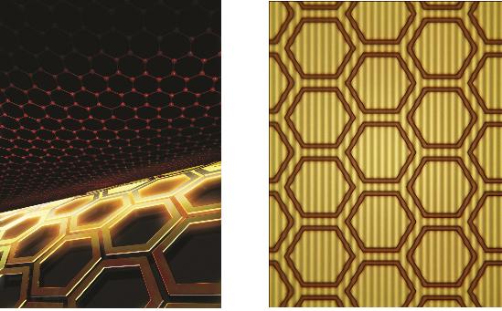
figure 1. The working drawing of graphene metamaterials
figure 2. Conceptual diagram (Left) and microscopic photo (right) of graphene metamaterials
2012.11.23 View 12342
The control of light at the nano-level
Professor Min Bumki
Professor Min Bumki’s research team from the Department of Mechanical Engineering at KAIST have successfully gained control of the transmittance of light in optical devices using graphene* and artificial 2-dimensional metamaterials**.
* Graphene : a thin membrane composed of pure carbon, with atoms arranged in a regular hexagonal pattern
** Metamaterials : artificial materials engineered to have properties that may not be found in nature
The research results were published in the recent online edition (September 30th) of Nature Materials, a sister journal of the world renowned Nature journal, under the title ‘Terahertz waves with gate-controlled active graphene metamaterials’
Since the discovery of graphene in 2004 by Professors Novoselov and Geim from the University of Manchester (2010 Nobel Prize winners in Physics), it has been dubbed “the dream material” because of its outstanding physical properties.
Graphene has been especially praised for its ability to absorb approximately 2.3% of near infrared and visible rays due to its characteristic electron structure. This property allows graphene to be used as a transparent electrode, which is a vital electrical component used in touch screens and solar batteries. However, graphene’s optical transmittance was largely ignored by researchers due to its limited control using electrical methods and its small optical modulation in data transfer.
Professor Min’s team combined 0.34 nanometer-thick graphene with metamaterials to allow a more effective control of light transmittance and greater optical modulation. This graphene metamaterial can be integrated in to a thin and flexible macromolecule substrate which allows the control of transmittance using electric signals.
This research experimentally showed that graphene metamaterials can not only effective control optical transmittance, but can also be used in graphene optical memory devices using electrical hysteresis.
Professor Min said that “this research allows the effective control of light at the nanometer level” and that “this research will help in the development of microscopic optical modulators or memory disks”.
figure 1. The working drawing of graphene metamaterials
figure 2. Conceptual diagram (Left) and microscopic photo (right) of graphene metamaterials
2012.11.23 View 12342